©
1988 Burr-Brown Corporation
PDS-872G
Printed in U.S.A. September, 1993
DESCRIPTION
The OPA620 is a precision wideband monolithic opera-
tional amplifier featuring very fast settling time, low
differential gain and phase error, and high output
current drive capability.
The OPA620 is internally compensated for unity-gain
stability. This amplifier has a very low offset, fully
symmetrical differential input due to its "classical"
operational amplifier circuit architecture. Unlike "cur-
rent-feedback" amplifier designs, the OPA620 may be
OPA620
Current
Mirror
Output
Stage
C
C
3
2
Non-Inverting
Input
Inverting
Input
7
+V
CC
4
≠V
CC
6 Output
Æ
used in all op amp applications requiring high speed
and precision.
Low noise and distortion, wide bandwidth, and high
linearity make this amplifier suitable for RF and video
applications. Short-circuit protection is provided by an
internal current-limiting circuit.
The OPA620 is available in plastic and ceramic DIP
and SO-8 packages. Two temperature ranges are of-
fered: ≠40
∞
C to +85
∞
C and ≠55
∞
C to +125
∞
C.
APPLICATIONS
q
LOW NOISE PREAMPLIFIER
q
LOW NOISE DIFFERENTIAL AMPLIFIER
q
HIGH-RESOLUTION VIDEO
q
HIGH-SPEED SIGNAL PROCESSING
q
LINE DRIVER
q
ADC/DAC BUFFER
q
ULTRASOUND
q
PULSE/RF AMPLIFIERS
q
ACTIVE FILTERS
Wideband Precision
OPERATIONAL AMPLIFIER
FEATURES
q
LOW NOISE: 2.3nV/
Hz
q
HIGH OUTPUT CURRENT: 100mA
q
FAST SETTLING: 25ns (0.01%)
q
GAIN-BANDWIDTH PRODUCT: 200MHz
q
UNITY-GAIN STABLE
q
LOW OFFSET VOLTAGE:
±
200
µ
V
q
LOW DIFFERENTIAL GAIN/PHASE ERROR
q
8-PIN DIP, SO-8 PACKAGES
International Airport Industrial Park ∑ Mailing Address: PO Box 11400, Tucson, AZ 85734 ∑ Street Address: 6730 S. Tucson Blvd., Tucson, AZ 85706 ∑ Tel: (520) 746-1111 ∑ Twx: 910-952-1111
Internet: http://www.burr-brown.com/ ∑ FAXLine: (800) 548-6133 (US/Canada Only) ∑ Cable: BBRCORP ∑ Telex: 066-6491 ∑ FAX: (520) 889-1510 ∑ Immediate Product Info: (800) 548-6132
OPA620
OPA620
OPA620
SBOS162
Æ
OPA620
2
OPA620KP, KU
OPA620SG
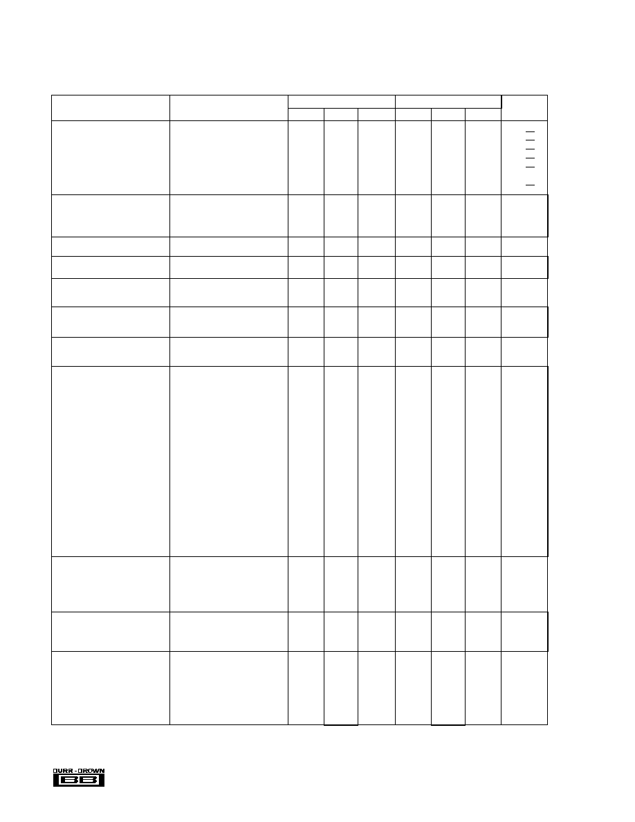
PARAMETER
CONDITIONS
MIN
TYP
MAX
MIN
TYP
MAX
UNITS
INPUT NOISE
Voltage: f
O
= 100Hz
R
S
= 0
10
T
nV/
Hz
f
O
= 1kHz
5.5
T
nV/
Hz
f
O
= 10kHz
3.3
T
nV/
Hz
f
O
= 100kHz
2.5
T
nV/
Hz
f
O
= 1MHz to 100MHz
2.3
T
nV/
Hz
f
B
= 100Hz to 10MHz
8.0
T
µ
Vr ms
Current: f
O
= 10kHz to 100MHz
2.3
T
pA/
Hz
OFFSET VOLTAGE
(1)
Input Offset Voltage
V
CM
= 0VDC
±
200
±
1000
T
T
µ
V
Average Drift
T
A
= T
MIN
to T
MAX
±
8
T
µ
V/
∞
C
Supply Rejection
±
V
CC
= 4.5V to 5.5V
50
60
T
T
dB
BIAS CURRENT
Input Bias Current
V
CM
= 0VDC
15
30
T
T
µ
A
OFFSET CURRENT
Input Offset Current
V
CM
= 0VDC
0.2
2
T
T
µ
A
INPUT IMPEDANCE
Differential
Open-Loop
15 ||
1
T
k
||
pF
Common-Mode
1 ||
1
T
M
||
pF
INPUT VOLTAGE RANGE
Common-Mode Input Range
±
3.0
±
3.5
T
T
V
Common-Mode Rejection
V
IN
=
±
2.5VDC, V
O
= 0VDC
65
75
T
T
dB
OPEN-LOOP GAIN, DC
Open-Loop Voltage Gain
R
L
= 100
50
60
T
T
dB
R
L
= 50
48
58
T
T
dB
FREQUENCY RESPONSE
Closed-Loop Bandwidth
Gain = +1V/V
300
T
MHz
(≠3dB)
Gain = +2V/V
100
T
MHz
Gain = +5V/V
40
T
MHz
Gain = +10V/V
20
T
MHz
Gain-Bandwidth Product
Gain
+5V/V
200
T
MHz
Differential Gain
3.58MHz, G = +1V/V
0.05
T
%
Differential Phase
3.58MHz, G = +1V/V
0.05
T
Degrees
Harmonic Distortion
(2)
G = +2V/V, f = 10MHz, V
O
= 2Vp-p
Second Harmonic
≠61
≠50
T
T
dBc
(3)
Third Harmonic
≠65
≠55
T
T
dBc
Full Power Bandwidth
(2)
V
O
= 5Vp-p, Gain = +1V/V
11
16
T
T
MHz
V
O
= 2Vp-p, Gain = +1V/V
27
40
T
T
MHz
Slew Rate
(2)
2V Step, Gain = ≠1V/V
175
250
T
T
V/
µ
s
Overshoot
2V Step, Gain = ≠1V/V
10
T
%
Settling Time: 0.1%
2V Step, Gain = ≠1V/V
13
T
ns
0.01%
25
T
ns
Phase Margin
Gain = +1V/V
60
T
Degrees
Rise Time
Gain = +1V/V, 10% to 90%
V
O
= 100mVp-p; Small Signal
2
T
ns
V
O
= 6Vp-p; Large Signal
22
T
ns
RATED OUTPUT
Voltage Output
R
L
= 100
±
3.0
±
3.5
T
T
V
R
L
= 50
±
2.5
±
3.0
T
T
V
Output Resistance
1MHz, Gain = +1V/V
0.015
T
Load Capacitance Stability
Gain = +1V/V
20
T
pF
Short Circuit Current
Continuous
±
150
T
mA
POWER SUPPLY
Rated Voltage
±
V
CC
5
T
VDC
Derated Performance
±
V
CC
4.0
6.0
T
T
VDC
Current, Quiescent
I
O
= 0mA
21
23
T
T
mA
TEMPERATURE RANGE
Specification: KP, KU
Ambient Temperature
≠40
+85
T
T
∞
C
SG
≠55
+125
∞
C
Operating: SG
Ambient Temperature
≠55
+125
∞
C
KP, KU
≠40
+85
∞
C
JA
: SG
125
∞
C/W
KP
90
∞
C/W
KU
100
∞
C/W
ELECTRICAL
At V
CC
=
±
5VDC, R
L
= 100
, and T
A
= +25
∞
C, unless otherwise noted.
SPECIFICATIONS
The information provided herein is believed to be reliable; however, BURR-BROWN assumes no responsibility for inaccuracies or omissions. BURR-BROWN assumes no responsibility
for the use of this information, and all use of such information shall be entirely at the user's own risk. Prices and specifications are subject to change without notice. No patent rights or
licenses to any of the circuits described herein are implied or granted to any third party. BURR-BROWN does not authorize or warrant any BURR-BROWN product for use in life support
devices and/or systems.
3
Æ
OPA620
SPECIFICATIONS (
CONT
)
ELECTRICAL (FULL TEMPERATURE RANGE SPECIFICATIONS)
At V
CC
=
±
5VDC, R
L
= 100
, and T
A
= T
MIN
to T
MAX
, unless otherwise noted.
TEMPERATURE RANGE
Specification: KP, KU
Ambient Temperature
≠40
+85
T
T
∞
C
SG
≠55
+125
∞
C
OFFSET VOLTAGE
(1)
Average Drift
Full Temp.
±
8
T
µ
V/
∞
C
Supply Rejection
0
∞
C to +70
∞
C
±
V
CC
= 4.5V to 5.5V
45
60
T
T
dB
Full Temp.,
±
V
CC
= 4.5 to 5.5V
40
55
T
T
dB
BIAS CURRENT
Input Bias Current
Full Temp., V
CM
= 0VDC
15
40
T
T
µ
A
OFFSET CURRENT
Input Offset Current
Full Temp., V
CM
= 0VDC
0.2
5
T
T
µ
A
INPUT VOLTAGE RANGE
Common-Mode Input Range
±
2.5
±
3.0
T
T
V
Common-Mode Rejection
V
IN
=
±
2.5VDC, V
O
= 0VDC
60
75
T
T
dB
OPEN LOOP GAIN, DC
Open-Loop Voltage Gain
R
L
= 100
46
60
T
T
dB
R
L
= 50
44
58
T
T
dB
RATED OUTPUT
Voltage Output
0
∞
C to +70
∞
C, R
L
= 100
±
3.0
±
3.5
T
T
V
≠40
∞
C to +85
∞
C, R
L
= 100
±
2.75
±
3.25
T
T
V
0
∞
C to +70
∞
C, R
L
= 50
±
2.5
±
3.0
T
T
V
≠40
∞
C to +85
∞
C, R
L
= 50
±
2.25
±
2.7
T
T
V
POWER SUPPLY
Current, Quiescent
I
O
= 0mA
21
25
T
T
mA
OPA620KP, KU
OPA620SG
PARAMETER
CONDITIONS
MIN
TYP
MAX
MIN
TYP
MAX
UNITS
T
Same specifications as for KP, KU.
NOTES: (1) Offset Voltage specifications are also guaranteed with units fully warmed up. (2) Parameter is guaranteed by characterization. (3) dBc = dB referred
to carrier-input signal.
PIN CONFIGURATION
Top View
DIP/SO-8
1
2
3
4
8
7
6
5
No Internal Connection
Positive Supply (+V )
Output
No Internal Connection
No Internal Connection
Inverting Input
Non-Inverting Input
Negative Supply (≠V )
CC
CC
OPA620
Basic Model Number
Performance Grade Code
K = ≠40
∞
C to +85
∞
C
S = ≠55
∞
C to +125
∞
C
Package Code
G = 8-pin Ceramic DIP
P = 8-pin Plastic DIP
U = SO-8 Surface Mount
ORDERING INFORMATION
(
)
(
)
ABSOLUTE MAXIMUM RATINGS
Supply .............................................................................................
±
7VDC
Internal Power Dissipation
(1)
....................... See Applications Information
Differential Input Voltage ............................................................ Total V
CC
Input Voltage Range .................................... See Applications Information
Storage Temperature Range: SG ................................. ≠65
∞
C to +150
∞
C
KP, KU .......................... ≠40
∞
C to +125
∞
C
Lead Temperature (soldering, 10s) .............................................. +300
∞
C
(soldering, SO-8, 3s) ...................................... +260
∞
C
Output Short Circuit to Ground (+25
∞
C) ............... Continuous to Ground
Junction Temperature (T
J
) ............................................................ +175
∞
C
NOTE: (1) Packages must be derated based on specified
JA
. Maximum T
J
must be observed.
PACKAGE INFORMATION
PACKAGE DRAWING
PRODUCT
PACKAGE
NUMBER
(1)
OPA620KP
8-Pin Plastic DIP
006
OPA620KU
SO-8 Surface Mount
182
OPA620SG
8-Pin Ceramic DIP
157
NOTE: (1) For detailed drawing and dimension table, please see end of data
sheet, or Appendix C of Burr-Brown IC Data Book.
ELECTROSTATIC
DISCHARGE SENSITIVITY
This integrated circuit can be damaged by ESD. Burr-Brown
recommends that all integrated circuits be handled with
appropriate precautions. Failure to observe proper handling and
installation procedures can cause damage.
ESD damage can range from subtle performance degradation to
complete device failure. Precision integrated circuits may be more
susceptible to damage because very small parametric changes
could cause the device not to meet its published specifications.
Æ
OPA620
4
TYPICAL PERFORMANCE CURVES
(CONT)
At V
CC
=
±
5VDC, R
L
= 100
, and T
A
= +25
∞
C, unless otherwise noted.
OPEN-LOOP FREQUENCY RESPONSE
Frequency (Hz)
1k
10k
100k
1M
10M
100M
1G
80
60
40
20
0
-20
Open-Loop Voltage Gain (dB)
Gain
Phase
Phase
Margin
60∞
0
≠45
≠90
≠135
≠180
Phase Shift (∞)
A = +1V/V CLOSED-LOOP
SMALL-SIGNAL BANDWIDTH
V
Frequency (Hz)
+4
+2
0
≠4
≠6
≠8
1M
10M
100M
1G
0
≠45
≠90
≠135
≠180
Gain (dB)
≠2
Phase Shift (∞)
A
OL
PM 60∞
Gain
Open-Loop Phase
A = +2V/V CLOSED-LOOP
SMALL-SIGNAL BANDWIDTH
V
Frequency (Hz)
+10
+8
+6
+2
0
≠2
1M
10M
100M
1G
0
≠45
≠90
≠135
≠180
Gain (dB)
+4
Phase Shift (∞)
A
OL
PM 70∞
Gain
Open-Loop Phase
A
V
= +10V/V CLOSED-LOOP
SMALL-SIGNAL BANDWIDTH
Frequency (Hz)
+24
+22
+20
+16
+14
+12
1M
10M
100M
1G
0
≠45
≠90
≠135
≠180
Gain (dB)
+18
Phase Shift (∞)
OL
Gain
Open-Loop Phase
A
PM 90∞
A = +1V/V CLOSED-LOOP BANDWIDTH
vs OUTPUT VOLTAGE SWING
V
Frequency (Hz)
8
6
0
1M
10M
100M
1G
Output Voltage (Vp-p)
4
1k
10k
100k
2
R = 50
L
A = +2V/V CLOSED-LOOP BANDWIDTH
vs OUTPUT VOLTAGE SWING
V
Frequency (Hz)
8
6
0
1M
10M
100M
1G
Output Voltage (Vp-p)
4
1k
10k
100k
2
R = 50
L
5
Æ
OPA620
TYPICAL PERFORMANCE CURVES
(CONT)
At V
CC
=
±
5VDC, R
L
= 100
, and T
A
= +25
∞
C, unless otherwise noted.
6
1
INPUT OFFSET VOLTAGE WARM-UP DRIFT
+100
+50
0
≠50
≠100
0
2
3
4
5
Offset Voltage Change (µV)
Time from Power Turn-on (min)
INPUT VOLTAGE AND CURRENT NOISE
SPECTRAL DENSITY vs TEMPERATURE
3.1
2.8
2.5
2.2
1.9
≠75
≠50
≠25
0
+25
+50
+75
+100
+125
2.9
2.6
2.3
2.0
1.7
Voltage Noise (nV/
Hz)
Current Noise (pA/
Hz)
Ambient Temperature (∞C)
f = 100kHz
O
Current Noise
Voltage Noise
TOTAL INPUT VOLTAGE NOISE SPECTRAL DENSITY
vs SOURCE RESISTANCE
Frequency (Hz)
100
0.1
1M
10M
100M
Voltage Noise (nV/ Hz)
10
100
1k
10k
1
100k
R = 1k
S
R = 500
S
S
R = 0
S
R = 100
A = +10V/V CLOSED-LOOP BANDWIDTH
vs OUTPUT VOLTAGE SWING
V
Frequency (Hz)
8
6
0
1M
10M
100M
1G
Output Voltage (Vp-p)
4
1k
10k
100k
2
R = 50
L
INPUT CURRENT NOISE SPECTRAL DENSITY
Frequency (Hz)
100
0.1
1M
10M
100M
10
100
1k
10k
1
100k
Current Noise (pA/
Hz)
0
INPUT OFFSET VOLTAGE CHANGE
DUE TO THERMAL SHOCK
+1000
+500
0
≠500
≠1000
≠1
+1
+2
+3
+4
Offset Voltage Change (µV)
Time from Thermal Shock (min)
+5
K Grade
T = 25∞C to 70∞C
Air Environment
A
SG T = 25∞C to T = 125∞C
Air Environment
A
A
25∞C
Æ
OPA620
6
TYPICAL PERFORMANCE CURVES
(CONT)
At V
CC
=
±
5VDC, R
L
= 100
, and T
A
= +25
∞
C, unless otherwise noted.
COMMON-MODE REJECTION vs FREQUENCY
Frequency (Hz)
1k
10k
100k
1M
10M
100M
1G
80
60
40
20
0
-20
Common-Mode Rejection (dB)
V = 0VDC
O
≠4
COMMON-MODE REJECTION
vs INPUT COMMON-MODE VOLTAGE
80
75
70
65
60
≠5
≠2
0
+2
+3
Common-Mode Rejection (dB)
Common-Mode Voltage (V)
+5
≠3
≠1
+1
+4
V = 0VDC
O
≠3
BIAS AND OFFSET CURRENT
vs INPUT COMMON-MODE VOLTAGE
25
20
15
10
9
≠4
≠2
≠1
0
+1
+2
+3
0.8
0.6
0.4
0.2
0
Bias Current (µA)
Offset Current (µA)
Common-Mode Voltage (V)
Bias Current
+4
Offset Current
≠50
BIAS AND OFFSET CURRENT
vs TEMPERATURE
21
18
15
12
9
≠75
≠25
0
+25
+50
+75
+100
0.8
0.6
0.4
0.2
0
Bias Current (µA)
Offset Current (µA)
Ambient Temperature (∞C)
+125
Bias Current
Offset Current
POWER SUPPLY REJECTION vs FREQUENCY
Frequency (Hz)
1k
10k
100k
1M
10M
100M
1G
80
60
40
20
0
-20
Power Supply Rejection (dB)
+ PSR
≠ PSR
≠50
SUPPLY CURRENT vs TEMPERATURE
25
23
21
19
17
≠75
≠25
0
+25
+50
+75
+100
Supply Current (mA)
Ambient Temperature (∞C)
+125

7
Æ
OPA620
TYPICAL PERFORMANCE CURVES
(CONT)
At V
CC
=
±
5VDC, R
L
= 100
, and T
A
= +25
∞
C, unless otherwise noted.
≠50
A , PSR, AND CMR vs TEMPERATURE
80
70
60
50
40
≠75
≠25
0
+25
+50
+75
+100
A , PSR, CMR (dB)
Temperature (∞C)
+125
OL
OL
A
OL
PSR
CMR
≠50
FREQUENCY CHARACTERISTICS vs TEMPERATURE
2.0
1.5
1.0
0.5
0
≠75
≠25
0
+25
+50
+75
+100
Relative Value
Temperature (∞C)
+125
Gain-Bandwidth
Slew Rate
Settling Time
SETTLING TIME vs OUTPUT VOLTAGE CHANGE
160
140
80
40
0
0
2
4
6
Settling Time (ns)
Output Voltage Change (V)
100
8
120
60
20
G = ≠1V/V
0.01%
0.1%
≠2
SETTLING TIME vs CLOSED-LOOP GAIN
100
80
40
20
0
≠1
≠3
≠4
≠5
≠6
≠7
≠9
Settling Time (ns)
Closed-Loop Amplifier Gain (V/V)
60
≠8
V = 2V Step
O
≠10
0.01%
0.1%
SMALL-SIGNAL TRANSIENT RESPONSE
≠50
0
+50
0
25
50
Time (ns)
0
LARGE-SIGNAL TRANSIENT RESPONSE
100
200
Time (ns)
+3
0
≠3
G = +1V/V
R
L
= 50
C
L
= 15pF
G = +1V/V
R
L
= 50
C
L
= 15pF
Output Voltage (mV)
Output Voltage (mV)
Æ
OPA620
8
TYPICAL PERFORMANCE CURVES
(CONT)
At V
CC
=
±
5VDC, R
L
= 100
, and T
A
= +25
∞
C, unless otherwise noted.
SMALL-SIGNAL
HARMONIC DISTORTION vs FREQUENCY
≠30
≠50
≠60
≠80
100k
Harmonic Distortion (dBc)
Frequency (Hz)
100M
≠40
≠70
1M
10M
G = +2V/V
R = 50
L
O
V = 0.5Vp-p
2f
3f
1MHz HARMONIC DISTORTION
vs POWER OUTPUT
≠30
≠50
≠60
≠80
≠20
Harmonic Distortion (dBc)
Power Output (dBm)
+15
≠40
≠70
0
+5
≠90
≠15
+10
≠10
≠5
0.125Vp-p
0.25Vp-p
0.5Vp-p
1Vp-p
2Vp-p
G = +2V/V
R = 50
L
C
f = 1MHz
3f
2f
LARGE-SIGNAL
HARMONIC DISTORTION vs FREQUENCY
≠30
≠50
≠60
≠80
100k
Harmonic Distortion (dBc)
Frequency (Hz)
100M
≠40
≠70
1M
10M
G = +2V/V
R = 50
L
O
V = 2Vp-p
2f
3f
10MHz HARMONIC DISTORTION
vs POWER OUTPUT
≠30
≠50
≠60
≠80
≠20
Harmonic Distortion (dBc)
Power Output (dBm)
+15
≠40
≠70
0
+5
≠90
≠15
+10
≠10
≠5
0.125Vp-p
0.25Vp-p
0.5Vp-p
1Vp-p
2Vp-p
G = +2V/V
R = 50
L
C
f = 10MHz
2f
3f
NTSC DIFFERENTIAL GAIN vs CLOSED-LOOP GAIN
0.5
0.3
0.2
0
1
3
6
8
Differential Gain (%)
Closed-Loop Amplifier Gain (V/V)
10
0.4
0.1
2
4
5
7
9
f = 3.58MHz
R = 75 (Two Back-Terminated Outputs)
L
V = 0V to 0.7V
O
V = 0V to 2.1V
O
V = 0V to 1.4V
O
NTSC DIFFERENTIAL PHASE vs CLOSED-LOOP GAIN
1.0
0.6
0.4
0
1
3
6
8
Differential Phase (Degrees)
Closed-Loop Amplifier Gain (V/V)
10
0.8
0.2
2
4
5
7
9
f = 3.58MHz
R = 75 (Two Back-Terminated Outputs)
L
V = 0V to 0.7V
O
V = 0V to 2.1V
O
V = 0V to 1.4V
O

9
Æ
OPA620
Oscillations at frequencies of 200MHz and above can easily
occur if good grounding techniques are not used. A heavy
ground plane (2 oz. copper recommended) should connect
all unused areas on the component side. Good ground planes
can reduce stray signal pickup, provide a low resistance, low
inductance common return path for signal and power, and
can conduct heat from active circuit package pins into
ambient air by convection.
Supply bypassing is extremely critical and must always be
used, especially when driving high current loads. Both
power supply leads should be bypassed to ground as close as
possible to the amplifier pins. Tantalum capacitors (1
µ
F to
10
µ
F) with very short leads are recommended. A parallel
0.1
µ
F ceramic should be added at the supply pins. Surface
mount bypass capacitors will produce excellent results due
to their low lead inductance. Additionally, suppression fil-
ters can be used to isolate noisy supply lines. Properly
bypassed and modulation-free power supply lines allow full
amplifier output and optimum settling time
performance.
Points to Remember
1) Don't use point-to-point wiring as the increase in wiring
inductance will be detrimental to AC performance. How-
ever, if it must be used, very short, direct signal paths are
required. The input signal ground return, the load ground
return, and the power supply common should all be
connected to the same physical point to eliminate ground
loops, which can cause unwanted feedback.
2) Good component selection is essential. Capacitors used in
critical locations should be a low inductance type with a high
quality dielectric material. Likewise, diodes used in critical
locations should be Schottky barrier types, such as HP5082-
2835 for fast recovery and minimum charge storage.
Ordinary diodes will not be suitable in RF circuits.
3) Whenever possible, solder the OPA620 directly into the
PC board without using a socket. Sockets add parasitic
capacitance and inductance, which can seriously degrade
AC performance or produce oscillations. If sockets must be
used, consider using zero-profile solderless sockets such as
Augat part number 8134-HC-5P2. Alternately, Teflon
Æ
stand-
offs located close to the amplifier's pins can be used to
mount feedback components.
4) Resistors used in feedback networks should have values
of a few hundred ohms for best performance. Shunt capaci-
tance problems limit the acceptable resistance range to about
1k
on the high end and to a value that is within the
amplifier's output drive limits on the low end. Metal film
and carbon resistors will be satisfactory, but wirewound
resistors (even "non-inductive" types) are absolutely
unacceptable in high-frequency circuits.
5) Surface-mount components (chip resistors, capacitors,
etc) have low lead inductance and are therefore strongly
recommended. Circuits using all surface-mount components
with the OPA620KU (SO-8 package) will offer the best AC
performance. The parasitic package inductance and capaci-
tance for the SO-8 is lower than the both the Cerdip and
8-lead Plastic DIP.
APPLICATIONS INFORMATION
DISCUSSION OF PERFORMANCE
The OPA620 provides a level of speed and precision not
previously attainable in monolithic form. Unlike current
feedback amplifiers, the OPA620's design uses a "classical"
operational amplifier architecture and can therefore be used
in all traditional operational amplifier applications. While it
is true that current feedback amplifiers can provide wider
bandwidth at higher gains, they offer many disadvantages.
The asymmetrical input characteristics of current feedback
amplifiers (i.e., one input is a low impedance) prevents them
from being used in a variety of applications. In addition,
unbalanced inputs make input bias current errors difficult to
correct. Bias current cancellation through matching of in-
verting and non-inverting input resistors is impossible
because the input bias currents are uncorrelated. Current
noise is also asymmetrical and is usually significantly higher
on the inverting input. Perhaps most important, settling time
to 0.01% is often extremely poor due to internal design
tradeoffs. Many current feedback designs exhibit settling
times to 0.01% in excess of 10 microseconds even though
0.1% settling times are reasonable. Such amplifiers are
completely inadequate for fast settling 12-bit applications.
The OPA620's "classical" operational amplifier architecture
employs true differential and fully symmetrical inputs to
eliminate these troublesome problems. All traditional circuit
configurations and op amp theory apply to the OPA620. The
use of low-drift thin-film resistors allows internal operating
currents to be laser-trimmed at wafer-level to optimize AC
performance such as bandwidth and settling time, as well as
DC parameters such as input offset voltage and drift. The
result is a wideband, high-frequency monolithic operational
amplifier with a gain-bandwidth product of 200MHz, a
0.01% settling time of 25ns, and an input offset voltage
of 200
µ
V.
WIRING PRECAUTIONS
Maximizing the OPA620's capability requires some wiring
precautions and high-frequency layout techniques.
Oscillation, ringing, poor bandwidth and settling, gain
peaking, and instability are typical problems plaguing all
high-speed amplifiers when they are improperly used. In
general, all printed circuit board conductors should be wide
to provide low resistance, low impedance signal paths. They
should also be as short as possible. The entire physical
circuit should be as small as practical. Stray capacitances
should be minimized, especially at high impedance nodes,
such as the amplifier's input terminals. Stray signal coupling
from the output or power supplies to the inputs should be
minimized. All circuit element leads should be no longer
than 1/4 inch (6mm) to minimize lead inductance, and low
values of resistance should be used. This will minimize time
constants formed with the circuit capacitances and will
eliminate stray, parasitic circuits.
Grounding is the most important application consideration
for the OPA620, as it is with all high-frequency circuits.
Teflon
Æ
E. I. Du Pont de Nemours & Co.
Æ
OPA620
10
6) Avoid overloading the output. Remember that output
current must be provided by the amplifier to drive its own
feedback network as well as to drive its load. Lowest
distortion is achieved with high impedance loads.
7) Don't forget that these amplifiers use
±
5V supplies.
Although they will operate perfectly well with +5V and
≠5.2V, use of
±
15V supplies will destroy the part.
8) Standard commercial test equipment has not been
designed to test devices in the OPA620's speed range.
Benchtop op amp testers and ATE systems will require a
special test head to successfully test these amplifiers.
9) Terminate transmission line loads. Unterminated lines,
such as coaxial cable, can appear to the amplifier to be a
capacitive or inductive load. By terminating a transmission
line with its characteristic impedance, the amplifier's load
then appears purely resistive.
10) Plug-in prototype boards and wire-wrap boards will not
be satisfactory. A clean layout using RF techniques is
essential; there are no shortcuts.
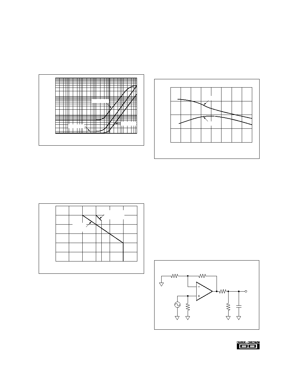
OFFSET VOLTAGE ADJUSTMENT
The OPA620's input offset voltage is laser-trimmed and
will require no further adjustment for most applications.
However, if additional adjustment is needed, the circuit in
Figure 1 can be used without degrading offset drift with
temperature. Avoid external adjustment whenever possible
since extraneous noise, such as power supply noise, can be
inadvertently coupled into the amplifier's inverting input
terminal. Remember that additional offset errors can be
created by the amplifier's input bias currents. Whenever
possible, match the impedance seen by both inputs as is
shown with R
3.
This will reduce input bias current errors to
the amplifier's offset current, which is typically only 0.2
µ
A.
FIGURE 1. Offset Voltage Trim.
NOTE: (1) R
3
is optional and can be used to cancel offset errors due to input
bias currents.
R
2
OPA620
(1)
R = R || R
3
1
2
R
1
R
Trim
+V
CC
≠V
CC
20k
V or Ground
IN
Output Trim Range +V ( R ) to ≠V ( R )
CC
2
2
CC
R
Trim
R
Trim
47k
INPUT PROTECTION
Static damage has been well recognized for MOSFET
devices, but any semiconductor device deserves protection
from this potentially damaging source. The OPA620 incor-
porates on-chip ESD protection diodes as shown in Figure 2.
This eliminates the need for the user to add external protec-
tion diodes, which can add capacitance and degrade AC
performance.
All pins on the OPA620 are internally protected from ESD
by means of a pair of back-to-back reverse-biased diodes to
either power supply as shown. These diodes will begin to
conduct when the input voltage exceeds either power
supply by about 0.7V. This situation can occur with loss of
the amplifier's power supplies while a signal source is still
present. The diodes can typically withstand a continuous
current of 30mA without destruction. To insure long term
reliability, however, diode current should be externally lim-
ited to 10mA or so whenever possible.
FIGURE 2. Internal ESD Protection.
ESD Protection diodes internally
connected to all pins.
External
Pin
+V
CC
≠V
CC
Internal
Circuitry
The internal protection diodes are designed to withstand
2.5kV (using Human Body Model) and will provide ad-
equate ESD protection for most normal handling proce-
dures. However, static damage can cause subtle changes in
amplifier input characteristics without necessarily destroy-
ing the device. In precision operational amplifiers, this may
cause a noticeable degradation of offset voltage and drift.
Therefore, static protection is strongly recommended when
handling the OPA620.
OUTPUT DRIVE CAPABILITY
The OPA620's design uses large output devices and has
been optimized to drive 50
and 75
resistive loads. The
device can easily drive 6Vp-p into a 50
load. This high-
output drive capability makes the OPA620 an ideal choice
for a wide range of RF, IF, and video applications. In many
cases, additional buffer amplifiers are unneeded.
Internal current-limiting circuitry limits output current to
about 150mA at 25
∞
C. This prevents destruction from
accidental shorts to common and eliminates the need for
external current-limiting circuitry. Although the device can
withstand momentary shorts to either power supply, it is not
recommended.
11
Æ
OPA620
Many demanding high-speed applications such as ADC/
DAC buffers require op amps with low wideband output
impedance. For example, low output impedance is essential
when driving the signal-dependent capacitances at the inputs
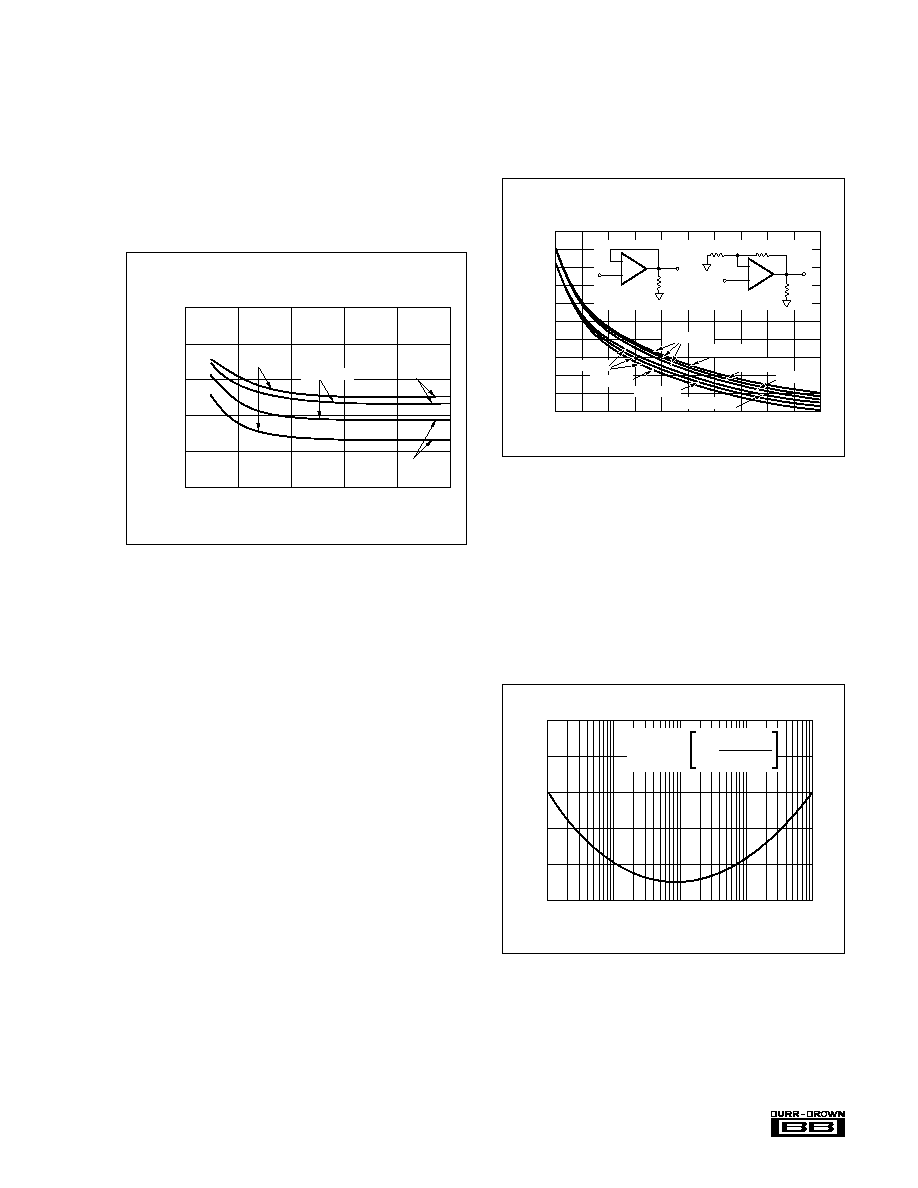
of flash A/D converters. As shown in Figure 3, the OPA620
maintains very low closed-loop output impedance over
frequency. Closed-loop output impedance increases with
frequency since loop gain is decreasing with frequency.
100
1k
10k
100k
1M
10M
100M
Frequency (Hz)
10
1
0.1
0.01
Small-Signal Output Impedance ( )
G = +10V/V
G = +1V/V
G = +2V/V
FIGURE 3. Small-Signal Output Impedance vs Frequency.
THERMAL CONSIDERATIONS
The OPA620 does not require a heat sink for operation in
most environments. The use of a heat sink, however, will
reduce the internal thermal rise and will result in cooler,
more reliable operation. At extreme temperatures and under
full load conditions a heat sink is necessary. See "Maximum
Power Dissipation" curve, Figure 4.
FIGURE 4. Maximum Power Dissipation.
The internal power dissipation is given by the equation P
D
=
P
DQ
+ P
DL
, where P
DQ
is the quiescent power dissipation and
P
DL
is the power dissipation in the output stage due to the
load. (For
±
V
CC
=
±
5V, P
DQ
= 10V x 23mA = 230mW, max).
For the case where the amplifier is driving a grounded load
(R
L
) with a DC voltage (
±
V
OUT
) the maximum value of P
DL
occurs at
±
V
OUT
=
±
V
CC
/2, and is equal to P
DL
, max =
(
±
V
CC
)
2
/4R
L
. Note that it is the voltage across the output
transistor, and not the load, that determines the power
dissipated in the output stage.
When the output is shorted to ground, P
DL
= 5V
x
150mA =
750mW. Thus, P
D
= 230mW + 750mW
1W. Note that the
short-circuit condition represents the maximum amount of
internal power dissipation that can be generated. Thus, the
"Maximum Power Dissipation" curve starts at 1W and is
derated based on a 175
∞
C maximum junction temperature
and the junction-to-ambient thermal resistance,
JA
, of each
package. The variation of short-circuit current with tempera-
ture is shown in Figure 5.
FIGURE 6. Driving Capacitive Loads.
OPA620
C
L
R
L
R
S
(R typically 5 to 25 )
S
CAPACITIVE LOADS
The OPA620's output stage has been optimized to drive
resistive loads as low as 50
. Capacitive loads, however,
will decrease the amplifier's phase margin which may cause
high frequency peaking or oscillations. Capacitive loads
greater than 20pF should be buffered by connecting a small
resistance, usually 5
to 25
, in series with the output as
shown in Figure 6. This is particularly important when
driving high capacitance loads such as flash A/D converters.
In general, capacitive loads should be minimized for
optimum high frequency performance. Coax lines can be
driven if the cable is properly terminated. The capacitance of
coax cable (29pF/foot for RG-58) will not load the amplifier
when the coaxial cable or transmission line is terminated in
its characteristic impedance.
FIGURE 5. Short-Circuit Current vs Temperature.
250
200
150
100
50
≠75
≠50
≠25
0
+25
+50
+75
+100
+125
Short-Circuit Current (mA)
Ambient Temperature (∞C)
+I
SC
≠ I
SC
Cerdip
Package
1.2
1.0
0.8
0.6
0.4
0.2
0
0
+25
+50
+75
+100
+125
+150
Ambient Temperature (∞C)
Internal Power Dissipation (W)
Plastic DIP, SO-8
Packages

Æ
OPA620
12
tors, which settle to 0.01% in sufficient time, are scarce and
expensive. Fast oscilloscopes, however, are more commonly
available. For best results, a sampling oscilloscope is recom-
mended. Sampling scopes typically have bandwidths that
are greater than 1GHz and very low capacitance inputs.
They also exhibit faster settling times in response to signals
that would tend to overload a real-time oscilloscope.
Figure 7 shows the test circuit used to measure settling time
for the OPA620. This approach uses a 16-bit sampling
oscilloscope to monitor the input and output pulses. These
waveforms are captured by the sampling scope, averaged,
and then subtracted from each other in software to produce
the error signal. This technique eliminates the need for the
traditional "false-summing junction," which adds extra para-
sitic capacitance. Note that instead of an additional flat-top
generator, this technique uses the scope's built-in calibration
source as the input signal.
COMPENSATION
The OPA620 is internally compensated and is stable in unity
gain with a phase margin of approximately 60
∞
. However,
the unity gain buffer is the most demanding circuit configu-
ration for loop stability and oscillations are most likely to
occur in this gain. If possible, use the device in a noise gain
of two or greater to improve phase margin and reduce the
susceptibility to oscillation. (Note that, from a stability
standpoint, an inverting gain of ≠1V/V is equivalent to a
noise gain of 2.) Gain and phase response for other gains are
shown in the Typical Performance Curves.
The high-frequency response of the OPA620 in a good
layout is very flat with frequency. However, some circuit
configurations such as those where large feedback
resistances are used, can produce high-frequency gain peak-
ing. This peaking can be minimized by connecting a small
capacitor in parallel with the feedback resistor. This capaci-
tor compensates for the closed-loop, high frequency, transfer
function zero that results from the time constant formed by
the input capacitance of the amplifier (typically 2pF after PC
board mounting), and the input and feedback resistors. The
selected compensation capacitor may be a trimmer, a fixed
capacitor, or a planned PC board capacitance. The capaci-
tance value is strongly dependent on circuit layout and
closed-loop gain. Using small resistor values will preserve
the phase margin and avoid peaking by keeping the break
frequency of this zero sufficiently high. When high closed-
loop gains are required, a three-resistor attenuator (tee
network) is recommended to avoid using large value
resistors with large time constants.
SETTLING TIME
Settling time is defined as the total time required, from the
input signal step, for the output to settle to within the
specified error band around the final value. This error band
is expressed as a percentage of the value of the output
transition, a 2V step. Thus, settling time to 0.01% requires
an error band of
±
200
µ
V centered around the final value
of 2V.
Settling time, specified in an inverting gain of one, occurs in
only 25ns to 0.01% for a 2V step, making the OPA620 one
of the fastest settling monolithic amplifiers commercially
available. Settling time increases with closed-loop gain and
output voltage change as described in the Typical Perform-
ance Curves. Preserving settling time requires critical
attention to the details as mentioned under "Wiring Precau-
tions." The amplifier also recovers quickly from input
overloads. Overload recovery time to linear operation from
a 50% overload is typically only 30ns.
In practice, settling time measurements on the OPA620
prove to be very difficult to perform. Accurate measurement
is next to impossible in all but the very best equipped labs.
Among other things, a fast flat-top generator and high speed
oscilloscope are needed. Unfortunately, fast flat-top genera-
NOTE: Test fixture built using all surface-mount components. Ground
plane used on component side and entire fixture enclosed in metal case.
Both power supplies bypassed with 10
µ
F Tantalum || 0.01
µ
F ceramic
capacitors. It is directly connected (without cable) to TIME CAL trigger
source on Sampling Scope (Data Precision's Data 6100 with Model
640-1 plug-in). Input monitored with Active Probe (Channel 1).
FIGURE 7. Settling Time Test Circuit.
OPA620
0 to ≠2V
V
OUT
To Active Probe
(Channel 2)
on sampling scope.
100
100
V
IN
0 to +2V, f = 1.25MHz
+5VDC
≠5VDC
2pF to 5pF (Adjust for Optimum Settling)
DIFFERENTIAL GAIN AND PHASE
Differential Gain (DG) and Differential Phase (DP) are
among the more important specifications for video applica-
tions. DG is defined as the percent change in closed-loop
gain over a specified change in output voltage level. DP is
defined as the change in degrees of the closed-loop phase
over the same output voltage change. Both DG and DP are
specified at the NTSC sub-carrier frequency of 3.58MHz.
DG and DP increase with closed-loop gain and output
voltage transition as shown in the Typical Performance
Curves. All measurements were performed using a Tektronix
model VM700 Video Measurement Set.
13
Æ
OPA620
DISTORTION
The OPA620's harmonic distortion characteristics into a
50
load are shown vs frequency and power output in the
Typical Performance Curves. Distortion can be further im-
proved by increasing the load resistance as illustrated in
Figure 8. Remember to include the contribution of the
feedback resistance when calculating the effective load
resistance seen by the amplifier.
FIGURE 8. 10MHz Harmonic Distortion vs Load Resistance.
G = +1V/V
V = 2Vp-p
O
10MHz HARMONIC DISTORTION
vs LOAD RESISTANCE
≠40
≠50
≠60
≠70
≠80
≠90
0
100
200
300
400
500
Harmonic Distortion (dBc)
Load Resistance ( )
G = +2V/V
3f
2f
Two-tone third-order intermodulation distortion (IM) is an
important parameter for many RF amplifier applications.
Figure 9 shows the OPA620's two-tone third-order IM
intercept vs frequency. For these measurements, tones were
spaced 1MHz apart. This curve is particularly useful for
determining the magnitude of the third-order IM products as
a function of frequency, load resistance, and gain. For
example, assume that the application requires the OPA620
to operate in a gain of +2V/V and drive 2Vp-p (4dBm for
each tone) into 50
at a frequency of 10MHz. Referring to
Figure 9 we find that the intercept point is +40dBm. The
magnitude of the third-order IM products can now be easily
calculated from the expression:
Third IMD = 2(OPI
3
P ≠ P
O
)
where OPI
3
P = third-order output intercept, dBm
P
O
= output level/tone, dBm/tone
Third IMD = third-order intermodulation ratio
below each output tone, dB
For this case OPI
3
P = 40dBm, P
O
= 4dBm, and the third-
order IMD = 2(40 ≠ 10) = 72dB below either 4dBm tone.
The OPA620's low IMD makes the device an excellent
choice for a variety of RF signal processing applications.
FIGURE 9. 2-Tone, 3rd Order Intermodulation Intercept vs
Frequency.
0
10
20
30
40
50
60
70
80
90
100
10
15
20
25
30
35
40
45
50
55
G = +1V/V
R
L
P
OUT
P
OUT
250
250
R
L
60
≠
≠
+
+
G = +2V/V
G = +1V/V
Frequency (MHz)
Intercept Point (+dBm)
R = 50
L
R = 100
L
G = +2V/V
R = 50
L
R = 100
L
R = 400
L
R = 400
L
2-TONE, 3
RD
ORDER INTERMODULATION
INTERCEPT vs FREQUENCY
NOISE FIGURE
The OPA620's voltage and current noise spectral densities
are specified in the Typical Performance Curves. For RF
applications, however, Noise Figure (NF) is often the
preferred noise specification since it allows system noise
performance to be more easily calculated. The OPA620's
Noise Figure vs Source Resistance is shown in Figure 10.
NOISE FIGURE vs SOURCE RESISTANCE
25
20
15
10
5
0
10
100
1k
10k
100k
NF (dB)
Source Resistance ( )
NF
dB
= 10log 1 +
e
n
2
+ (i
n
R
S
)
2
4kTR
S
FIGURE 10. Noise Figure vs Source Resistance.

Æ
OPA620
14
SPICE MODELS
Computer simulation using SPICE is often useful when
analyzing the performance of analog circuits and systems.
This is particularly true for Video and RF amplifier circuits
where parasitic capacitance and inductance can have a major
effect on circuit performance. A SPICE model using
MicroSim Corporation's PSpice is available for the OPA620.
This simulation model is available through the Burr-Brown
web site at www.burr-brown.com or by contacting the Burr-
Brown Applications Department.
RELIABILITY DATA
Extensive reliability testing has been performed on the
OPA620. Accelerated life testing (2000 hours) at maximum
operating temperature was used to calculate MTTF at an
ambient temperature of 25
∞
C. These test results yield MTTF
of: Cerdip package = 1.31E+9 Hours, Plastic DIP = 5.02E+7
Hours, and SO-8 = 2.94E+7 Hours. Additional tests such as
PCT have also been performed. Reliability reports are avail-
able upon request for each of the package options offered.
DEMONSTRATION BOARDS
Demonstration boards are available to speed protyping. The
8-pin DIP packaged parts may be evaluated using the DEM-
OPA65XP board while the SO-8 packaged part may be
evaluated using the DEM-OPA65XU board. Both of these
boards come partially assembled from your local distributor
(the external resistors and the amplifier are not included).
FIGURE 13. Low Noise, Wideband FET Input Op Amp.
FIGURE 12. High-Q 1MHz Bandpass Filter.
* Select J
1
, J
2
and R
1
, R
2
to set
input stage current for optimum
performance.
I
B
e
N
Gain-Bandwidth
Slew Rate
Settling Time
: 1pA
: 6nV/
Hz at 1MHz
: 200MHz
: 250 V/
µ
s
: 15ns to 0.1%
Feedback from pin 6 to the (≠) FET
input required for stability.
f
C
= 1MHz
BW = 20kHz at ≠3dB
Q
= 50
OPA620
OPA620
2k
V
OUT
R
3
R
4
2k
158
R
5
C
2
15.8k
R
1
R
2
158
V
IN
1000pF
C
1000pF
1
OPA620
V
OUT
*R
1
2k
+5V
(≠)
(+)
D
S
*J
1
D
S
2N5911
≠5V
2
3
7
6
4
*R
2
2k
*J
2
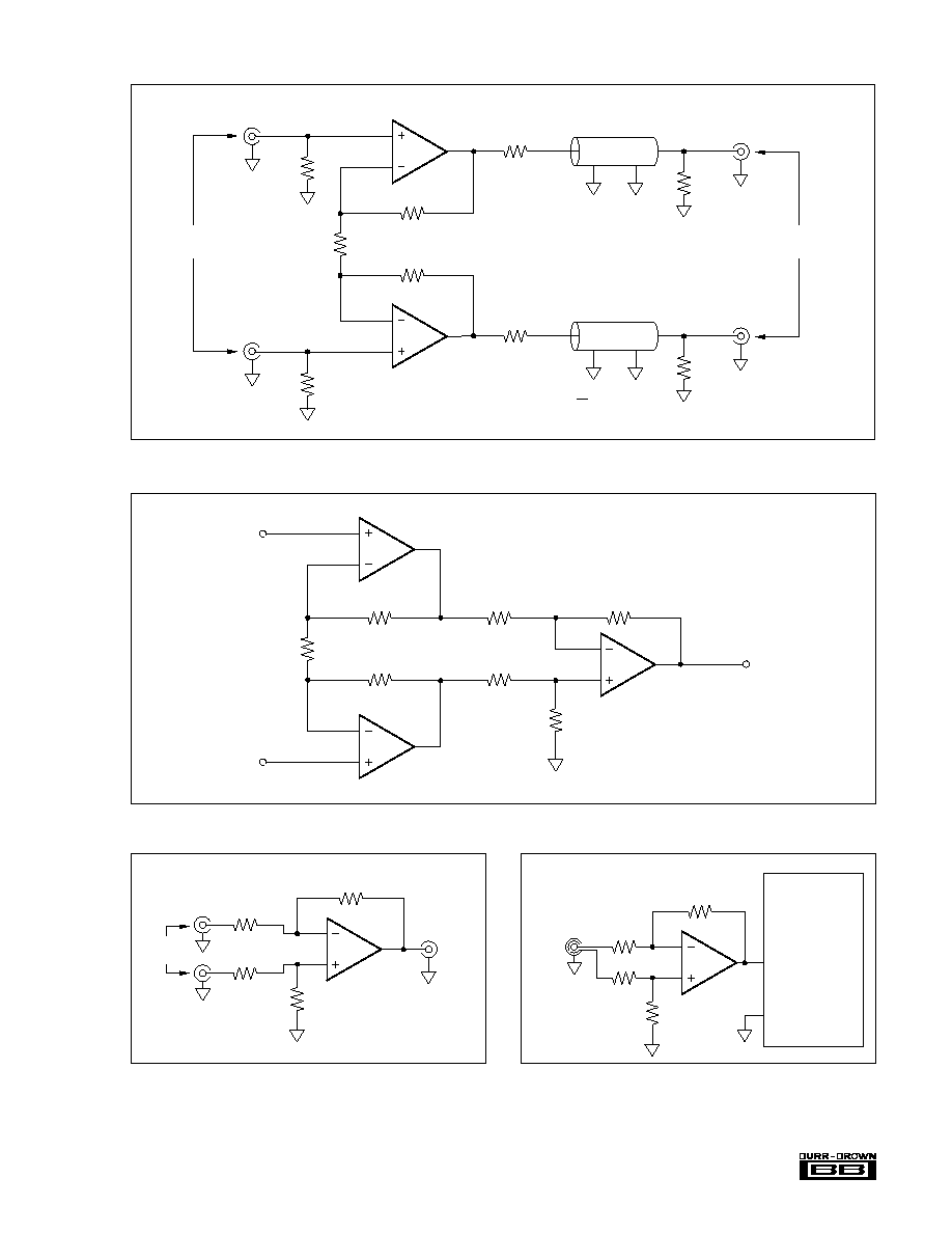
FIGURE 11. Video Distribution Amplifier.
High output current drive capability (6Vp-p into 50
)
allows three back-terminated 75
transmission lines
to be simultaneously driven.
OPA620
V
OUT
390
390
Video
Input
75
75
75 Transmission Line
V
OUT
75
75
V
OUT
75
75
75
APPLICATIONS
15
Æ
OPA620
FIGURE 14. Differential Line Driver for 50
or 75
Systems.
FIGURE 15. Wideband, Fast-Settling Instrumentation Amplifier.
Differential Voltage Gain = 2V/V = 1 + 2R
F
/R
G
OPA620
499
OPA620
249
R
F
249
R
G
249
R
F
249
OPA620
249
249
FIGURE 16. Unity Gain Difference Amplifier.
OPA620
249
249
Single-
Ended
Output
249
249
Differential
Input
FIGURE 17. Differential Input Buffer Amplifier (G = ≠2V/V).
OPA620
75
5
Signal
Input
150
10
75
Triax
Input
Analog
Common
ADS805
12-Bit,
10MHz A/D
Converter
OPA620
Differential
Input
50 or 75
Transmission Line
50
or
75
499
OPA620
249
50
or
75
R
F
249
R
F
50 or 75
50
or
75
50
or
75
Differential
Output
R
G
50 or 75
Transmission Line
50 or 75
Differential Voltage Gain =
Bandwidth, ≠3dB =
Slew Rate =
1
2
1V/V = (1 + 2R
F
/R
G
)
125MHz
500V/
µ
s

PACKAGING INFORMATION
ORDERABLE DEVICE
STATUS(1)
PACKAGE TYPE
PACKAGE DRAWING
PINS
PACKAGE QTY
OPA620KP
OBSOLETE
PDIP
P
8
OPA620KU
OBSOLETE
SOIC
D
8
OPA620KU/2K5
OBSOLETE
SOIC
D
8
(1) The marketing status values are defined as follows:
ACTIVE: Product device recommended for new designs.
LIFEBUY: TI has announced that the device will be discontinued, and a lifetime-buy period is in effect.
NRND: Not recommended for new designs. Device is in production to support existing customers, but TI does not recommend using this part in
a new design.
PREVIEW: Device has been announced but is not in production. Samples may or may not be available.
OBSOLETE: TI has discontinued the production of the device.
PACKAGE OPTION ADDENDUM
www.ti.com
3-Oct-2003

IMPORTANT NOTICE
Texas Instruments Incorporated and its subsidiaries (TI) reserve the right to make corrections, modifications,
enhancements, improvements, and other changes to its products and services at any time and to discontinue
any product or service without notice. Customers should obtain the latest relevant information before placing
orders and should verify that such information is current and complete. All products are sold subject to TI's terms
and conditions of sale supplied at the time of order acknowledgment.
TI warrants performance of its hardware products to the specifications applicable at the time of sale in
accordance with TI's standard warranty. Testing and other quality control techniques are used to the extent TI
deems necessary to support this warranty. Except where mandated by government requirements, testing of all
parameters of each product is not necessarily performed.
TI assumes no liability for applications assistance or customer product design. Customers are responsible for
their products and applications using TI components. To minimize the risks associated with customer products
and applications, customers should provide adequate design and operating safeguards.
TI does not warrant or represent that any license, either express or implied, is granted under any TI patent right,
copyright, mask work right, or other TI intellectual property right relating to any combination, machine, or process
in which TI products or services are used. Information published by TI regarding third-party products or services
does not constitute a license from TI to use such products or services or a warranty or endorsement thereof.
Use of such information may require a license from a third party under the patents or other intellectual property
of the third party, or a license from TI under the patents or other intellectual property of TI.
Reproduction of information in TI data books or data sheets is permissible only if reproduction is without
alteration and is accompanied by all associated warranties, conditions, limitations, and notices. Reproduction
of this information with alteration is an unfair and deceptive business practice. TI is not responsible or liable for
such altered documentation.
Resale of TI products or services with statements different from or beyond the parameters stated by TI for that
product or service voids all express and any implied warranties for the associated TI product or service and
is an unfair and deceptive business practice. TI is not responsible or liable for any such statements.
Following are URLs where you can obtain information on other Texas Instruments products and application
solutions:
Products
Applications
Amplifiers
amplifier.ti.com
Audio
www.ti.com/audio
Data Converters
dataconverter.ti.com
Automotive
www.ti.com/automotive
DSP
dsp.ti.com
Broadband
www.ti.com/broadband
Interface
interface.ti.com
Digital Control
www.ti.com/digitalcontrol
Logic
logic.ti.com
Military
www.ti.com/military
Power Mgmt
power.ti.com
Optical Networking
www.ti.com/opticalnetwork
Microcontrollers
microcontroller.ti.com
Security
www.ti.com/security
Telephony
www.ti.com/telephony
Video & Imaging
www.ti.com/video
Wireless
www.ti.com/wireless
Mailing Address:
Texas Instruments
Post Office Box 655303 Dallas, Texas 75265
Copyright
2003, Texas Instruments Incorporated