
Æ
OPA642
1
10MSPS
clk
402
24
1Vp-p
5MHz
OPA642
100pF
REFT
+5V
REFB
ADS804
12-Bit
10MSPS
Measured
80dB SFDR
Analog
Input
402
0.1µF
0.1µF
5k
High Dynamic Range 10MSPS Digitizer
5k
0.1µF
2Vp-p
+5V
≠5V
International Airport Industrial Park ∑ Mailing Address: PO Box 11400, Tucson, AZ 85734 ∑ Street Address: 6730 S. Tucson Blvd., Tucson, AZ 85706 ∑ Tel: (520) 746-1111 ∑ Twx: 910-952-1111
Internet: http://www.burr-brown.com/ ∑ FAXLine: (800) 548-6133 (US/Canada Only) ∑ Cable: BBRCORP ∑ Telex: 066-6491 ∑ FAX: (520) 889-1510 ∑ Immediate Product Info: (800) 548-6132
Wideband, Low Distortion, Low Gain
OPERATIONAL AMPLIFIER
APPLICATIONS
q
ADC/DAC BUFFER AMPLIFIER
q
LOW DISTORTION IF AMPLIFIER
q
HIGH RESOLUTION IMAGING
q
MEDICAL IMAGING
q
LOW NOISE PREAMPLIFIER
q
HIGH CMR DIFFERENCING AMPLIFIER
q
TEST INSTRUMENTATION
q
PROFESSIONAL AUDIO
FEATURES
q
LOW DISTORTION: ≠95dBc at 5MHz
q
GAIN OF +1 BANDWIDTH: 400MHz
q
AVAILABLE IN SOT23-5 PACKAGE
q
HIGH OPEN LOOP GAIN: 95dB
q
HIGH COMMON-MODE REJECTION: 90dB
q
FAST 12-BIT SETTLING: 13ns (0.01%)
q
LOW NOISE: 2.7nV/
Hz
q
HIGH OUTPUT CURRENT:
±
60mA
q
VERY LOW DIFF GAIN/PHASE ERROR:
0.007%/0.008
∞
Æ
OPA642
OPA642
OPA658
OPA642
DESCRIPTION
The OPA642 provides a level of speed and dynamic
range previously unattainable in a monolithic op amp.
Using a unity gain stable voltage feedback architec-
ture with two internal gain stages, the OPA642 achieves
exceptionally low harmonic distortion over a wide
frequency range. The "classic" differential input pro-
vides all the familiar benefits of precision op amps,
such as bias current cancellation and very low invert-
ing current noise compared with wideband current
feedback op amps. Fast settling time, excellent differ-
ential gain/phase performance, low voltage noise and
high output current drive make the OPA642 ideal for
most high dynamic range applications.
Unity gain stability makes the OPA642 particularly
suitable for low gain differential amplifiers,
transimpedance amplifiers, gain of +2 video line driv-
ers, wideband integrators and low distortion ADC buff-
ers. Where higher gain or even lower harmonic distor-
tion is required, consider the OPA643--a higher gain-
bandwidth and lower noise version of the OPA642
©
1993 Burr-Brown Corporation
PDS-1190F
Printed in U.S.A. February, 1998
SBOS024
2
Æ
OPA642
OPA642P, U, N
OPA642PB, UB, NB
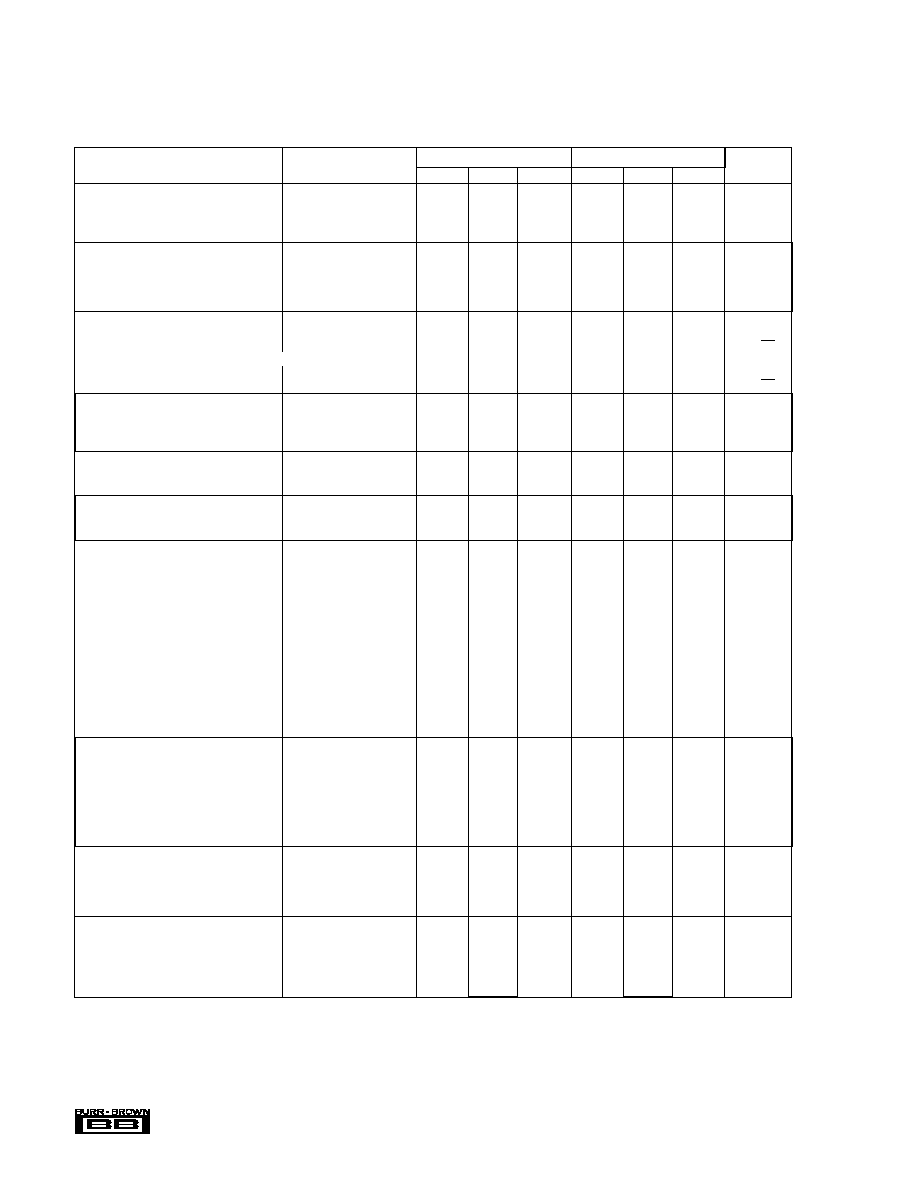
PARAMETER
CONDITIONS
MIN
TYP
MAX
MIN
TYP
MAX
UNITS
SPECIFICATIONS
ELECTRICAL
At T
A
= +25
∞
C, V
S
=
±
5V, R
L
= 100
, R
F
= 402
, unless otherwise noted. R
F
= 25
for a gain of +1.
OFFSET VOLTAGE
Input Offset Voltage
±
1.5
±
4
±
0.5
±
1.0
mV
Average Drift
4
2
µ
V/
∞
C
Power Supply Rejection (PSR)
V
S
=
±
4.5 to
±
5.5V
65
85
73
95
dB
INPUT BIAS CURRENT
Input Bias Current
V
CM
= 0V
25
45
T
T
µ
A
Over Specified Temperature
70
T
T
µ
A
Input Offset Current
V
CM
= 0V
0.1
2.0
T
T
µ
A
Over Specified Temperature
3.0
T
T
µ
A
NOISE
Input Voltage Noise
Noise Density: f
1MHz
2.7
T
nV/
Hz
Integrated Voltage Noise, BW = 100Hz to 100MHz
27
T
µ
Vrms
Input Bias Current Noise Density
f
1MHz
2.8
T
pA/
Hz
INPUT VOLTAGE RANGE
Common-Mode Input Range
±
2.75
±
3.0
T
T
V
Over Temperature
±
2.5
T
V
Common-Mode Rejection (CMR)
V
CM
=
±
0.5V
65
90
80
T
dB
INPUT IMPEDANCE
Differential
11 || 1
T
k
|| pF
Common-Mode
650 || 1
T
k
|| pF
OPEN-LOOP GAIN
Open-Loop Voltage Gain (A
OL
)
V
O
=
±
2V, R
L
= 100
80
95
85
98
dB
Over Specified Temperature
80
T
dB
FREQUENCY RESPONSE
Closed-Loop Response
Gain = +1V/V
400
T
MHz
Gain = +2V/V
150
T
MHz
Gain = +5V/V
45
T
MHz
Gain = +10V/V
21
T
MHz
Gain Bandwidth Product (GBP)
210
T
MHz
Slew Rate
(1)
G = +1, 2V Step
380
T
V/
µ
s
At Minimum Specified Temperature
G = +1, 2V Step
340
T
V/
µ
s
Settling Time: 0.01%
G = +1, 1V Step
13
T
ns
0.1%
G = +1, 1V Step
11.5
T
ns
1%
G = +1, 1V Step
3.5
T
ns
Spurious Free Dynamic Range (SFDR)
G = +1, f = 5MHz
92
95
dBc
V
O
= 2Vp-p, R
L
= 100
Diff. Gain Error at 3.58MHz, G = +2V/V
V
O
= 0V to 1.4V, R
L
= 150
0.007
T
%
Diff. Phase Error at 3.58MHz, G = +2V/V
V
O
= 0V to 1.4V, R
L
= 150
0.008
T
degrees
OUTPUT
Voltage Output
No Load
±
3.5
T
V
Over Specified Temperature
±
3.0
T
V
Voltage Output
R
L
= 100
±
2.75
T
V
Over Specified Temperature
±
2.5
T
T
V
Current Output, +25
∞
C
±
40
±
60
±
50
±
65
mA
Over Specified Temperature
±
35
±
40
mA
Closed-Loop Output Resistance
0.1MHz, G = +1V/V
0.01
T
POWER SUPPLY
Specified Operating Voltage
±
5
T
V
Operating Voltage Range
T
MIN
to T
MAX
±
4.5
±
5.5
T
T
V
Quiescent Current
±
20
±
25
±
16
T
T
mA
Over Specified Temperature
±
26
T
mA
TEMPERATURE RANGE
Specification: P, U, N, PB, UB, NB
Ambient
≠40
+85
T
T
∞
C
Thermal Resistance
JA
, Junction-to-Ambient
∞
C/W
P, PB
8-Pin DIP
100
T
∞
C/W
U, UB
8-Pin SO-8
125
T
∞
C/W
N, NB
5-Pin SOT23-5
150
T
∞
C/W
T
Indicates same specification as for OPA642P, U, N.
NOTE: (1) Slew rate is rate of change from 10% to 90% of output voltage step.

Æ
OPA642
3
Top View
DIP/SO-8
SOT23-5
The information provided herein is believed to be reliable; however, BURR-BROWN assumes no responsibility for inaccuracies or omissions. BURR-BROWN assumes
no responsibility for the use of this information, and all use of such information shall be entirely at the user's own risk. Prices and specifications are subject to change
without notice. No patent rights or licenses to any of the circuits described herein are implied or granted to any third party. BURR-BROWN does not authorize or warrant
any BURR-BROWN product for use in life support devices and/or systems.
ABSOLUTE MAXIMUM RATINGS
Supply ..........................................................................................
±
6.0VDC
Internal Power Dissipation
(1)
.................................. See Thermal Analysis
Differential Input Voltage ..................................................................
±
1.2V
Input Voltage Range ............................................................................
±
V
S
Storage Temperature Range: P, PB, U, UB, N, NB ..... ≠40
∞
C to +125
∞
C
Lead Temperature (soldering, 10s) .............................................. +300
∞
C
(soldering, SO-8 3s) ....................................... +260
∞
C
Junction Temperature (T
J
) ............................................................ +175
∞
C
NOTE: (1) Packages must be derated based on specified
JA
. Maximum
T
J
must be observed.
PIN CONFIGURATION
1
2
3
4
8
7
6
5
+V
S2
(1)
+V
S1
Output
≠V
S2
(1)
NC
Inverting Input
Non-Inverting Input
≠V
S1
NOTE: (1) Making use of all four power supply pins is recommended,
although not required. Using these four pins, instead of just pins 4 and 7, will
lower the power supply impedance improving distortion.
PACKAGE
DRAWING
TEMPERATURE
PACKAGE
ORDERING
PRODUCT
PACKAGE
NUMBER
(1)
RANGE
MARKING
(2)
NUMBER
(3)
OPA642U
SO-8 Surface Mount
182
≠40
∞
C to +85
∞
C
OPA642U
OPA642U
OPA642UB
SO-8 Surface Mount
182
≠40
∞
C to +85
∞
C
OPA642UB
OPA642UB
OPA642N
5-pin SOT23-5
331
≠40
∞
C to +85
∞
C
A42
OPA642N-250
OPA642N-3k
OPA642NB
5-pin SOT23-5
331
≠40
∞
C to +85
∞
C
A42B
OPA642NB-250
OPA642NB-3k
OPA642P
8-Pin Plastic DIP
006
≠40
∞
C to +85
∞
C
OPA642P
OPA642P
OPA642PB
8-Pin Plastic DIP
006
≠40
∞
C to +85
∞
C
OPA642PB
OPA642PB
NOTES: (1) For detailed drawing and dimension table, please see end of data sheet, or Appendix C of Burr-Brown IC Data Book. (2) The "B" grade of the SO-8 and
DIP packages will be marked with a "B" by pin 8. The "B" grade of the SOT23-5 will be marked with a "B" near pins 3 and 4. (3) The SOT23-5 is only available on a 7"
tape and reel (e.g. ordering 250 pieces of "OPA642N-250" will get a single 250 piece tape and reel. Ordering 3000 pieces of "OPA642N-3k" will get a single 3000 piece
tape and reel). Please refer to Appendix B of Burr-Brown IC Data Book for detailed Tape and Reel Mechanical information.
PACKAGE/ORDERING INFORMATION
ELECTROSTATIC
DISCHARGE SENSITIVITY
Electrostatic discharge can cause damage ranging from per-
formance degradation to complete device failure. Burr-
Brown Corporation recommends that all integrated circuits
be handled and stored using appropriate ESD protection
methods.
ESD damage can range from subtle performance degrada-
tion to complete device failure. Precision integrated circuits
may be more susceptible to damage because very small
parametric changes could cause the device not to meet
published specifications.
1
2
3
5
4
+V
S
Inverting Input
Output
≠V
S
Non-Inverting Input

4
Æ
OPA642
TYPICAL PERFORMANCE CURVES
At T
A
= +25
∞
C, V
S
=
±
5V, R
L
= 100
, R
F
= 402
,
G = +2, unless otherwise noted. R
F
= 25
for a gain of +1.
SMALL SIGNAL TRANSIENT RESPONSE
(G = +1, R
L
= 100
)
Time (5ns/div)
200
160
120
80
40
0
≠40
≠80
≠120
≠160
≠200
Output Voltage (mV)
LARGE SIGNAL TRANSIENT RESPONSE
(G = +1, R
L
= 100
)
Time (5ns/div)
2.0
1.6
1.2
0.8
0.4
0
≠0.4
≠0.8
≠1.2
≠1.4
≠2.0
Output Voltage (V)
LARGE SIGNAL FREQUENCY RESPONSE
Frequency
0.5MHz
10MHz
100MHz
500MHz
12
9
6
3
0
≠3
≠9
≠12
≠15
≠18
≠21
Gain (3dB/div)
G = +2
V
O
= 1Vp-p
V
O
= 2Vp-p
V
O
= 4Vp-p
R
S
vs CAPACITIVE LOAD
Capacitive Load (pF)
10
1
100
30
25
20
15
10
5
0
R
S
(
)
SMALL SIGNAL FREQUENCY RESPONSE
Frequency
0.5MHz
10MHz
100MHz
500MHz
6
3
0
≠3
≠6
≠9
≠12
≠15
≠18
≠21
≠24
Normalized Gain (3dB/div)
V
O
= 0.1Vp-p
G = +1
G = +2
G = +5
G = +10
FREQUENCY RESPONSE vs CAPACITIVE LOAD
Frequency (20MHz/div)
100MHz
0
200MHz
12
9
6
3
0
≠3
≠6
≠9
≠12
≠15
≠18
Gain to Capacitive Load (3dB/div)
C
L
= 10pF
G = +2
C
L
= 22pF
C
L
= 47pF
1k
402
(1k
is optional)
402
OPA642
R
S
C
L
V
IN
V
O
C
L
= 100pF

Æ
OPA642
5
TYPICAL PERFORMANCE CURVES
(CONT)
At T
A
= +25
∞
C, V
S
=
±
5V, R
L
= 100
, R
F
= 402
,
G = +2, unless otherwise noted. R
F
= 25
for a gain of +1.
5MHz 2ND HARMONIC DISTORTION
Output Voltage Swing (Vp-p)
1
0.1
10
G = +2
≠65
≠70
≠75
≠80
≠85
≠90
≠95
≠100
2nd Harmonic Distortion (dBc)
R
L
= 100
R
L
= 500
R
L
= 200
5MHz 3RD HARMONIC DISTORTION
Output Voltage Swing (Vp-p)
1
0.1
10
G = +2
≠65
≠70
≠75
≠80
≠85
≠90
≠95
≠100
3rd Harmonic Distortion (dBc)
R
L
= 100
, 200
, or 500
10MHz 3RD HARMONIC DISTORTION
Output Voltage Swing (Vp-p)
1
0.1
10
G = +2
≠60
≠65
≠70
≠75
≠80
≠85
≠90
≠95
≠100
3rd Harmonic Distortion (dBc)
R
L
= 100
R
L
= 200
R
L
= 500
20MHz 3RD HARMONIC DISTORTION
Output Voltage Swing (Vp-p)
1
0.1
10
G = +2
≠50
≠55
≠60
≠65
≠70
≠75
≠80
≠85
≠90
3rd Harmonic Distortion (dBc)
R
L
= 100
R
L
= 200
R
L
= 500
20MHz 2ND HARMONIC DISTORTION
Output Voltage Swing (Vp-p)
1
0.1
10
G = +2
≠50
≠55
≠60
≠65
≠70
≠75
≠80
≠85
≠90
2nd Harmonic Distortion (dBc)
R
L
= 200
R
L
= 500
R
L
= 100
10MHz 2ND HARMONIC DISTORTION
Output Voltage Swing (Vp-p)
1
0.1
10
≠60
≠65
≠70
≠75
≠80
≠85
≠90
≠95
≠100
2nd Harmonic Distortion (dBc)
G = +2
R
L
= 100
R
L
= 200
R
L
= 500

6
Æ
OPA642
TYPICAL PERFORMANCE CURVES
(CONT)
At T
A
= +25
∞
C, V
S
=
±
5V, R
L
= 100
, R
F
= 402
,
G = +2, unless otherwise noted. R
F
= 25
for a gain of +1.
0.006
0.004
0.002
≠0.000
≠0.002
≠0.004
0
0.7
1.4
DC Offset (V)
Differential Gain Error (%)
Differential Phase Error (
∞
)
0.008
0.006
0.004
0.002
0.000
0
0.7
1.4
DC Offset (V)
OPEN-LOOP GAIN AND PHASE
Frequency (Hz)
10
3
10
4
10
5
10
6
10
7
10
8
10
9
10
2
100
90
80
70
60
50
40
30
20
10
0
≠10
Open-Loop Gain (dB)
0
≠30
≠60
≠90
≠120
≠150
≠180
≠210
≠240
≠270
≠300
≠330
Open-Loop Phase (30∞/div)
Phase
Gain
TWO-TONE, THIRD ORDER
INTERMODULATION INTERCEPT
Frequency (MHz)
5
10
15
20
25
30
35
40
50
45
40
35
30
25
20
Intercept (dBm)
402
402
OPA642
50
50
50
P
i
P
O
2ND HARMONIC DISTORTION vs FREQUENCY
Frequency (MHz)
1
10
0.1
20
G = 2
≠40
≠50
≠60
≠70
≠80
≠90
≠100
2nd Harmonic Distortion (dBc)
V
O
= 2Vp-p
G = 8
G = 4
G = 1
3RD HARMONIC DISTORTION vs FREQUENCY
Frequency (MHz)
1
10
0.1
20
G = 8
≠40
≠50
≠60
≠70
≠80
≠90
≠100
3rd Harmonic Distortion (dBc)
V
O
= 2Vp-p
G = 4
G = 1
G = 2
INPUT VOLTAGE AND CURRENT NOISE DENSITY
Frequency (Hz)
100
10
1
voltage Noise nV/
Hz
10
2
10
3
10
4
10
5
10
6
10
7
Current Noise
Voltage Noise
2.8pA/
Hz
2.7nV/
Hz

Æ
OPA642
7
TYPICAL PERFORMANCE CURVES
(CONT)
At T
A
= +25
∞
C, V
S
=
±
5V, R
L
= 100
, R
F
= 402
,
G = +2, unless otherwise noted. R
F
= 25
for a gain of +1.
COMMON-MODE REJECTION
vs INPUT COMMON-MODE VOLTAGE
100
90
80
70
60
≠5
≠4
≠3
≠2
≠1
0
1
2
3
4
5
Common-Mode Voltage (V)
Common-Mode Rejection (dB)
A
OL
, PSR AND CMR vs TEMPERATURE
Temperature (∞C)
≠75
≠50
≠25
0
25
50
75
100
125
110
100
90
80
A
OL
, PSR, CMR (dB)
PSR+
A
OL
PSR≠
CMR
OUTPUT AND QUIESCENT CURRENT
vs TEMPERATURE
Ambient Temperature (∞C)
≠50
≠25
0
25
50
75
100
125
80
70
60
50
40
30
20
10
0
Output Current (mA)
I
O
+
I
O
≠
I
CC
CLOSED-LOOP OUTPUT IMPEDANCE
Frequency (MHz)
500
0
0.1
1
10
100
10
1
0.1
0.01
0.001
Output Impedance (
)
CMR AND PSR vs FREQUENCY
Frequency (Hz)
100
90
80
70
60
50
40
30
20
Rejection Ratio (dB)
10
2
10
3
10
4
10
5
10
6
10
7
10
8
CMR
PSR
DIFFERENTIAL AND COMMON-MODE
INPUT IMPEDANCE
Frequency (Hz)
1000
100
10
1
Impedance (k
)
10
2
10
3
10
4
10
5
10
6
10
7
10
8
Differential Input
Common-Mode Input

8
Æ
OPA642
Gain, = 1 +
V
O
V
I
R
F
R
G
V
O
50
≠V
S
+V
S
50
Load
V
I
OPA642
50
R
G
402
R
F
402
50
Source
0.1µF
3
2
4
7
6
8
5
2.2µF
+
2.2µF
0.1µF
+
0.1µF
0.1µF
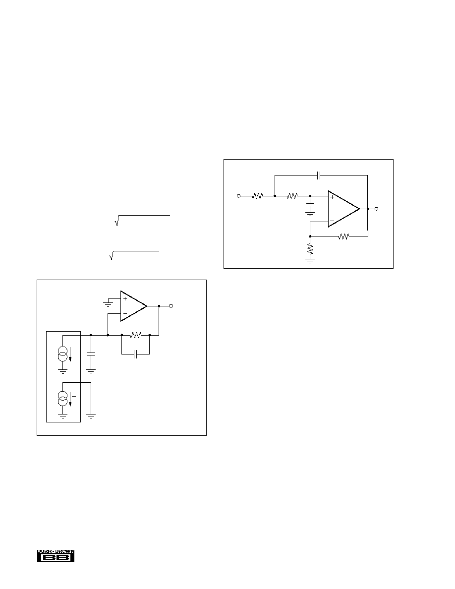
BUFFERING HIGH PERFORMANCE ADC'S
To achieve full performance from a high dynamic range
A/D converter, considerable care must be exercised in the
design of the input amplifier interface circuit. The example
circuit on the front page shows a typical AC-coupled inter-
face to a very high dynamic range converter. The frequency
domain application allows the OPA642 to be operated in its
most linear region, using a signal range which swings
symmetrically around ground (0V). The 2Vp-p swing is then
level-shifted through the blocking capacitor to a DC refer-
ence level, which is created by a well-decoupled resistive
divider off the converter's internal reference voltages. To
have a negligible effect on the rated spurious-free dynamic
range (SFDR) of the converter, the amplifier's SFDR should
be at least 10dB greater. In the front page example, the
insertion of the OPA642 has an immeasurable effect on the
distortion of the ADS804, which achieves 80dB SFDR at
5MHz Nyquist input signal.
To achieve the lowest possible distortion in the 8-pin SO-8
or DIP package, the addition of 0.1
µ
F decoupling capacitors
on pins 5 and 8 is required. These are shown in Figure 1.
Although pins 5 and 8 are internally connected to pins 4 and
7 respectively (the standard supply pins for 8-pin op amps),
the additional capacitors help to decouple the package lead
inductances and improve second harmonic suppression at
5MHz by approximately 4dB. The much shorter bond wires
and supply leads of the SOT23-5 package give the best
distortion performance while requiring only two power sup-
ply connections.
Successful application of the OPA642 for ADC buffering
requires careful selection of the series resistor at the ampli-
fier output, along with the additional shunt capacitor at the
ADC input. To some extent, selection of this RC network
will be determined empirically for each model of converter.
Many high performance CMOS ADCs, like the ADS804,
perform better with the shunt capacitor at the input pin. This
capacitor provides a low source impedance for the transient
currents produced by the sampling process. Improved SFDR
is obtained by adding the capacitor, whose value is often
recommended in the converter data sheet. The external
capacitor, in combination with the built-in capacitance of the
A/D input, presents a significant capacitive load to the
OPA642. Without a series isolation resistor, the result could
be undesirable peaking or loss of stability in the amplifier.
Since the DC bias current of the CMOS A/D input is
negligible, the resistor has no effect on overall gain or offset
accuracy. Refer to the plot of "R
S
vs Capacitive Load" in the
Typical Performance Curves to obtain a good starting value
for the series resistor. This will ensure flat frequency re-
sponse to the ADC input. Increasing the external capacitor
value will allow the series resistor to be reduced or, keeping
this resistor fixed, will band-limit the signal and reduce high
frequency noise to the input of the converter.
VIDEO LINE DRIVING
Most video distribution systems are designed with 75
series resistors to drive a matched 75
cable. In order to
deliver a net gain of 1 to the 75
matched load, the amplifier
FIGURE 1. Gain of +2, High Frequency Application and
Characterization Circuit [P or U Package].
APPLICATIONS INFORMATION
WIDEBAND VOLTAGE FEEDBACK OPERATION
The OPA642's combination of speed and dynamic range is
easily achieved in a wide variety of application circuits,
providing that simple principles of good design practice are
observed. For example, good power supply decoupling, as
shown in Figure 1, is essential to achieve the lowest possible
harmonic distortion and smooth frequency response. Proper
PC board layout and careful component selection will maxi-
mize the performance of the OPA642 in all applications, as
discussed in the remaining sections of this data sheet.
Figure 1 shows the gain of +2 configuration used as the basis
for most of the Typical Performance Curves. Most of the
curves were characterized using signal sources with 50
driving impedance, and with measurement equipment pre-
senting 50
shunt load impedance. In Figure 1, the 50
shunt resistor at the V
I
terminal matches the source imped-
ance of the test generator, while the 50
series resistor at the
V
O
terminal provides a matching resistor for the measure-
ment equipment load. Generally, data sheet specifications
refer to the voltage swing at the output pin (V
O
in Figure 1).
The 100
load from the series and shunt matching resis-
tances, combined with the 804
total feedback network
load, presents the OPA642 with an effective load of approxi-
mately 90
.

Æ
OPA642
9
is typically set up for a voltage gain of +2, compensating for
the 6dB attenuation of the voltage divider formed by the
series and shunt 75
resistors at either end of the cable. The
circuit of Figure 1 applies to this requirement if all refer-
ences to 50
resistors are replaced by 75
values. Often,
the amplifier gain is further increased to 2.2, which recovers
the additional DC loss of a typical long cable run. This
change would require the gain resistor (R
G
) in Figure 1 to be
reduced from 402
to 335
. In either case, both the gain
flatness and the differential gain/phase performance of the
OPA642 will provide exceptional results in video distribu-
tion applications. Differential Gain and Phase measure the
change in overall small-signal gain and phase for the color
subcarrier frequency (3.58MHz in NTSC systems) vs changes
in the large-signal output level (which represents luminance
information in a composite video signal). The OPA642, with
the typical 150
load of a single matched video cable,
shows less than 0.01%/0.01
∞
differential gain/phase errors
over the standard luminance range for a positive video
(negative sync) signal. Similar performance would be ob-
served for negative video signals. In practice, similar perfor-
mance is achieved even with two video loads due to the
linear high-frequency output impedance of the OPA642.
SINGLE OP-AMP DIFFERENTIAL AMPLIFIER
The voltage feedback architecture of the OPA642, with its
high CMR, will provide exceptional performance in differ-
ential amplifier configurations. Figure 2 shows a typical
configuration. The starting point for this design is the selec-
tion of the R
F
value in the range of 200
to 2k
. Lower
values reduce the required R
G
increasing the load on the V
2
source and on the OPA642 output. Higher values increase
output noise and exacerbate the effects of parasitic board
and device capacitances. Following the selection of R
F
, R
G
must be set to achieve the desired inverting gain for V
2
.
Remember that the bandwidth will be set approximately by
the gain bandwidth product (GBP) divided by the noise gain
(1+ R
F
/R
G
). For accurate differential operation (i.e. good
CMR), the ratio R
2
/R
1
must be set equal to R
F
/R
G
. Usually,
it is best to set the absolute values of R
2
and R
1
equal to R
F
and R
G
respectively; this equalizes the divider resistances
and cancels the effect of input bias currents. However, it is
sometimes useful to scale the values of R
2
and R
1
in order
to adjust the loading on the driving source V
1
. In most cases,
the achievable low frequency CMR will be limited by the
accuracy of the resistor values. The 90dB CMR of the
OPA642 itself will not determine the overall circuit CMR
unless the resistor ratios are matched to better than 0.003%.
If it is necessary to trim the CMR, then R
2
is the suggested
adjustment point.
THREE OP AMP DIFFERENCING
(Instrumentation Topology)
The primary drawback of the single op-amp differential
amplifier is its relatively low input impedances. Where a
high impedance is required at the differential input, a stan-
dard instrumentation amplifier (INA) topology may be built
using the OPA642 as the differencing stage. Figure 3 shows
an example of this, in which the two input amplifiers are
packaged together as a dual voltage feedback op-amp--the
OPA2650. This approach saves board space, cost and power
compared to using two additional OPA642 devices, and still
achieves very good noise and distortion performance due to
the moderate loading on the input amplifiers. In this circuit,
the common mode gain to the output is always one due to the
four matched 1k
resistors, while the differential gain is set
by (1 + 2R
F1
/R
G
)--which is equal to 2 using the values in
Figure 3. The differential to single-ended conversion is still
performed by the OPA642 output stage. The high imped-
ance inputs allow the V
1
and V
2
sources to be terminated or
impedance matched as required without further loading by
the differential amplifier. If the V
1
and V
2
inputs are already
truly differential, such as the output from a signal trans-
former, then a single matching termination resistor may be
used between them. Remember, however, that a defined DC
signal path must always exist for the V
1
and V
2
inputs; for
the transformer case, a center-tapped secondary connected
to ground would provide an optimum DC operating point.
FIGURE 3. Wideband 3-Op Amp Differencing Amplifier.
1/2
OPA2650
1/2
OPA2650
OPA642
1k
1k
1k
R
F1
500
R
F1
500
V
1
V
2
V
O
V
O
= 2 (V
1
≠ V
2
)
Power Supplies and
De-coupling Not Shown
R
G
1k
1k
V
O
= (V
1
≠ V
2
)
when =
R
F
R
G
R
2
R
1
R
F
R
G
R
F
≠5V
+5V
Power Supply
De-coupling Not Shown
R
G
V
2
V
1
R
1
OPA642
R
2
FIGURE 2. High Speed, Single Amplifier Differential
Amplifier.
10
Æ
OPA642
DAC TRANSIMPEDANCE AMPLIFIER
High frequency DDC DACs require a low distortion output
amplifier to retain their SFDR performance into real-world
loads. A single-ended output drive implementation is shown
in Figure 4. In this circuit, only one side of the complemen-
tary output drive signal is used. The diagram shows the
signal output current connected into the virtual ground
summing junction of the OPA642, which is set up as a
transimpedance stage or "I-V converter". The unused cur-
rent output of the DAC is connected to ground. If the DAC
requires its outputs terminated to a compliance voltage other
than ground for operation, then the appropriate voltage level
may be applied to the non-inverting input of the OPA642.
The DC gain for this circuit is equal to R
F
. At high frequen-
cies, the DAC output capacitance will produce a zero in the
noise gain for the OPA642 that may cause peaking in the
closed-loop frequency response. C
F
is added across R
F
to
compensate for this noise gain peaking. To achieve a flat
transimpedance frequency response, this pole in the feed-
back network should be set to:
which will give a corner frequency
-3dB
of approximately:
Figure 5 shows an example Sallen-Key low pass filter, in
which the OPA642 is set up to deliver a low frequency gain
of +2. The filter component values have been selected to
achieve a maximally flat Butterworth response with a 5MHz
≠3dB bandwidth. The resistor values have been slightly
adjusted to compensate for the effects of the 150MHz band-
width provided by the OPA642 in this configuration. This
filter may be combined with the ADC driver suggestions to
provide moderate (2-pole) Nyquist filtering, limiting noise
and out of band components into the input of an ADC. This
filter will deliver the exceptionally low harmonic distortion
required by high SFDR A/D converters such as the ADS804
(12-bit, 10MSPS, 80dB SFDR).
OPA642
High Speed
DAC
V
O
= I
O
R
F
R
F
C
F
GBP
Gain Bandwidth
Product for the OPA642
C
D
I
O
I
O
FIGURE 4. Wideband, Low Distortion DAC Transimpedance
Amplifier.
ACTIVE FILTERS
Most active filter topologies will deliver exceptional perfor-
mance using the broad bandwidth and unity gain stability of
the OPA642. Topologies employing capacitive feedback
require a unity gain stable voltage feedback op amp. Sallen-
Key filters simply use the op amp as a non-inverting gain
stage inside an RC network. Either current or voltage feed-
back op amps may be used in Sallen-Key implementations.
FIGURE 5. 5MHz Butterworth Low Pass Active Filter.
V
O
402
505
V
I
124
OPA642
100pF
402
150pF
OPERATING SUGGESTIONS
OPTIMIZING RESISTOR VALUES
Since the OPA642 is a unity gain stable voltage feedback op
amp, a wide range of resistor values may be used for the
feedback and gain setting resistors. The primary limits on
these values are set by dynamic range (noise and distortion)
and parasitic capacitance considerations. For a non-inverting
unity gain follower application, the feedback connection
should be made with a 25
resistor--not a direct short. This
will isolate the inverting input capacitance from the output
pin and improve the frequency response flatness. Usually,
the feedback resistor value should be between 200
and
1k
. Below 200
, the feedback network will present
additional output loading which can degrade the harmonic
distortion performance of the OPA642. Above 1k
, the
typical parasitic capacitance (approximately 0.2pF) across
the feedback resistor may cause unintentional band-limiting
in the amplifier response.
A good rule of thumb is to target the parallel combination of
R
F
and R
G
(Figure 1) to be less than about 200
. The
combined impedance R
F
|| R
G
interacts with the inverting
input capacitance, placing an additional pole in the feedback
network and thus a zero in the forward response. Assuming
a 2pF total parasitic on the inverting node, holding R
F
|| R
G
< 200
will keep this pole above 400MHz. By itself, this
constraint implies that the feedback resistor R
F
can increase
to several k
at high gains. This is acceptable as long as the
pole formed by R
F
and any parasitic capacitance appearing
in parallel is kept out of the frequency range of interest.
≠3dB
=
GBP / 2
R
F
C
D
1 / 2
R
F
C
F
=
GBP / 4
R
F
C
D
(
)

Æ
OPA642
11
In the inverting configuration, an additional design consid-
eration must be noted. R
G
becomes the input resistor and
therefore the load impedance to the driving source. If imped-
ance matching is desired, R
G
may be set equal to the
required termination value. However, at low inverting gains
the resultant feedback resistor value can present a significant
load to the amplifier output. For example, an inverting gain
of 2 with a 50
input matching resistor (= R
G
) would require
a 100
feedback resistor, which would contribute to output
loading in parallel with the external load. In such a case, it
would be preferable to increase both the R
F
and R
G
values,
and then achieve the input matching impedance with a third
resistor to ground. The total input impedance becomes the
parallel combination of R
G
and the additional shunt resistor.
BANDWIDTH VS GAIN
Voltage feedback op amps exhibit decreasing closed-loop
bandwidth as the signal gain is increased. In theory, this
relationship is described by the Gain Bandwidth Product
(GBP) shown in the specifications. Ideally, dividing GBP by
the non-inverting signal gain (also called the Noise Gain, or
NG) will predict the closed-loop bandwidth. In practice, this
only holds true when the phase margin approaches 90
∞
, as it
does in high gain configurations. At low signal gains, most
amplifiers will exhibit a more complex response with lower
phase margin. The OPA642 is optimized to give a maxi-
mally flat second order Butterworth response in a gain of 2.
In this configuration, the OPA642 has approximately 60
∞
of
phase margin and will show a typical ≠3dB bandwidth of
150MHz. When the phase margin is 60
∞
, the closed-loop
bandwidth is approximately
2 greater than the value pre-
dicted by dividing GBP by the noise gain. Increasing the
gain will cause the phase margin to approach 90
∞
and the
bandwidth to more closely approach the predicted value of
(GBP/NG). At a gain of +10, the 21MHz bandwidth shown
in the Typical Specifications agrees with that predicted
using the simple formula and the typical GBP of 210MHz.
OUTPUT DRIVE CAPABILITY
The OPA642 has been optimized to drive the demanding
load of a doubly terminated transmission line. When a 50
line is driven, a series 50
into the cable and a terminating
50
load at the end of the cable are used. Under these
conditions, the cable's impedance will appear resistive over
a wide frequency range, and the total effective load on the
OPA642 is 100
in parallel with the resistance of the
feedback network. The Specifications show a guaranteed
±
2.5V swing into a such a load--which will then be reduced
to a
±
1.25V swing at the termination resistor. The guaran-
teed
±
35mA output drive over temperature provides ad-
equate current drive margin for this load. Higher voltage
swings (and lower distortion) are achievable when driving
higher impedance loads.
A single video load typically appears as a 150
load (using
standard 75
cables) to the driving amplifier. The OPA642
provides adequate voltage and current drive to support up to
3 parallel video loads (50
total load) for an NTSC signal.
With only one load, the OPA642 achieves an exceptionally
low 0.007%/0.008
∞
dG/dP error.
DRIVING CAPACITIVE LOADS
One of the most demanding, and yet very common, load
conditions for an op amp is capacitive loading. A high speed,
high open-loop gain, amplifier like the OPA642 can be very
susceptible to decreased stability and closed-loop response
peaking when a capacitive load is placed directly on the
output pin. In simple terms, the capacitive load reacts with
the open-loop output resistance of the amplifier to introduce
an additional pole into the loop and thereby decrease the
phase margin. This issue has become a popular topic of
application notes and articles, and several external solutions
to this problem have been suggested. When the primary
considerations are frequency response flatness, pulse re-
sponse fidelity and/or distortion, the simplest and most
effective solution is to isolate the capacitive load from the
feedback loop by inserting a series isolation resistor between
the amplifier output and the capacitive load. This does not
eliminate the pole from the loop response, but rather shifts
it and adds a zero at a higher frequency. The additional zero
acts to cancel the phase lag from the capacitive load pole,
thus increasing the phase margin and improving stability.
The Typical Performance Curves show the recommended
R
S
vs Capacitive Load and the resulting frequency response
at the load. The criterion for setting the recommended
resistor is maximum bandwidth, flat frequency response at
the load. Since there is now a passive low pass filter between
the output pin and the load capacitance, the response at the
output pin itself is typically somewhat peaked, and becomes
flat after the rolloff action of the RC network. This is not a
concern in most applications, but can cause clipping if the
desired signal swing at the load is very close to the amplifier's
swing limit. Such clipping would be most likely to occur in
pulse response applications where the frequency peaking is
manifested as an overshoot in the step response.
Parasitic capacitive loads greater than 2pF can begin to
degrade the performance of the OPA642. Long PC board
traces, unmatched cables, and connections to multiple de-
vices can easily cause this value to be exceeded. Always
consider this effect carefully, and add the recommended
series resistor as close as possible to the OPA642 output pin
(see Board Layout Guidelines).
DISTORTION PERFORMANCE
The OPA642 is capable of delivering an exceptionally low
distortion signal at high frequencies and low gains. The
distortion plots in the Typical Performance Curves show the
typical distortion under a wide variety of conditions. Most of
these plots are limited to 100dB dynamic range. The
OPA642's distortion does not rise above ≠100dBc until
either the signal level exceeds 0.5V and/or the fundamental
frequency exceeds 500kHz. Distortion in the audio band is
≠120dBc.
Generally, until the fundamental signal reaches very high
frequencies or powers, the second harmonic will dominate the
distortion with negligible third harmonic component. Focus-
ing then on the second harmonic, increasing the load imped-
ance improves distortion directly. Remember that the total
load includes the feedback network--in the non-inverting

12
Æ
OPA642
NF
=
10 log 2
+
E
N
2
kTRs
configuration this is sum of R
F
+ R
G
, while in the inverting
configuration this is just R
F
(Figure 1). Increasing output
voltage swing increases harmonic distortion directly. A 6dB
increase in output swing will generally increase the second
harmonic 12dB and the third harmonic 18dB. Increasing the
signal gain will also increase the second harmonic distortion.
Again a 6dB increase in gain will increase the second and third
harmonic by 6dB even with a constant output power and
frequency. And finally, the distortion increases as the funda-
mental frequency increases due to the rolloff in the loop gain
with frequency. Conversely, the distortion will improve going
to lower frequencies down to the dominant open-loop pole at
approximately 3kHz. Starting from the ≠90dBc second har-
monic for 2Vp-p into 500
, G = +2 distortion at 1MHz (from
the Typical Performance Curves), the second harmonic distor-
tion at 20kHz should be approximately ≠90dB ≠ 20log
(1MHz/20kHz) = ≠124dBc.
The OPA642 has an extremely low third order harmonic
distortion. This also gives an exceptionally good two-tone,
third-order intermodulation intercept as shown in the Typi-
cal Performance Curves. This intercept curve is defined at
the 50
load when driven through a 50
matching resistor
to allow direct comparisons to RF MMIC devices. This
network attenuates the voltage swing from the output pin to
the load by 6dB. If the OPA642 drives directly into the input
of a high impedance device, such as an ADC, this 6dB
attenuation is not taken. Under these conditions, the inter-
cept will increase by a minimum 6dBm. The intercept is
used to predict the intermodulation spurious for two closely
spaced frequencies. If the two test frequencies, f1 and f2, are
specified in terms of average and delta frequency, f
O
= (f1
+ f2)/ 2 and
f = |f
2
≠ f
2
|
/2,
the two, third-order, close-in
spurious tones will appear at f
O
±
(3 ∑
f). The difference
between two equal test tone power levels and these
intermodulation spurious power levels is given by 2 ∑ (IM3
≠ P
O
) where IM3 is the intercept taken from the Typical
Performance Curve and P
O
is the power level in dBm at the
50
load for one of the two closely spaced test frequencies.
For instance, at 10MHz the OPA642 at a gain of +2 has an
intercept of 46dBm at a matched 50
load. If the full
envelope of the two frequencies needs to be 2Vp-p, this
requires each tone to be 4dBm. The third-order
intermodulation spurious tones will then be 2 ∑ (46 ≠ 4) =
84dBc below the test tone power level (≠80dBm). If this
same 2Vp-p two-tone envelope were delivered directly into
the input of an ADC without the matching loss or loading of
the 50
network, the intercept would increase to at least
52dBm. With the same signal and gain conditions but now
driving directly into a light load, the spurious tones will then
be at least 2 ∑ (52 ≠ 4) = 96dBc below the 1Vp-p test tone
signal levels.
NOISE PERFORMANCE
The OPA642 complements its ultra-low harmonic distortion
with low input noise terms. Both the input referred voltage
noise, and the two input referred current noise terms com-
bine to give a low output noise under a wide variety of
operating conditions. Figure 6 shows the op amp noise
analysis model with all the noise terms included. In this
model, all the noise terms are taken to be noise voltage or
current density terms in either nV/
Hz or pA/
Hz.
The total output spot noise voltage can be computed as the
square root of the squared contributing terms to the output
noise voltage. This computation is adding all the contribut-
ing noise powers at the output by superposition, then taking
the square root to get back to a spot noise voltage. Equation
1 shows the general form for this output noise voltage using
the terms shown in Figure 6.
E
O
=
E
NI
2
+
I
BN
R
S
(
)
2
+
4kTR
S
(
)
G
N
2
+
I
BI
R
F
(
)
2
+
4kTR
F
G
N
FIGURE 6. Op Amp Noise Analysis Model.
Dividing this expression by the noise gain (G
N
= 1 + R
F
/R
G
)
will give the equivalent input referred spot noise voltage at
the non-inverting input as shown in Equation 2.
E
N
=
E
NI
2
+
I
BN
R
S
(
)
2
+
4kTR
S
+
I
BI
R
F
G
N
2
+
4kTR
F
G
N
Evaluating these two equations for the OPA642 circuit
shown in Figure 1 will give a total output spot noise voltage
of 6.7nV/
Hz and an equivalent input spot noise voltage of
3.35nV/
Hz.
Narrowband communications systems are more commonly
concerned with the noise figure for the amplifier. The total
input referred voltage noise expression (Eq. 2), may be used
to calculate the noise figure. Equation 3 shows this noise
figure expression using the E
N
of Eq. 2 for the non-inverting
configuration where the input terminating resistor R
T
has been
set to match the source impedance (as shown in Figure 1).
Evaluating Equation 3 for the circuit of Figure 1 gives a
Noise Figure = 17.6dB. Input transformer coupling can be
used to reduce this noise figure. A broadband pulse trans-
former can provide both a noiseless voltage gain and a more
optimum source impedance to minimize the noise figure.
Figure 7 shows an example built from the circuit of Figure
1, in which the transformer turns ratio has been set to the
Eq. 1
Eq. 2
Eq. 3
4kT
R
G
R
G
R
F
R
S
OPA642
I
BI
E
O
I
BN
4kT = 1.6E ≠20J
at 290∞K
E
RS
E
NI
4kTR
S
4kTR
F

Æ
OPA642
13
FIGURE 8. DC Coupled, Inverting Gain of ≠2, with Output
Offset Adjustment.
closest integer for minimum noise figure. This optimum
turns ratio is calculated by
This optimum will depend strongly on the amplifier and
configuration selected.
the offset control is best applied as an inverting summing
signal. If the signal path is intended to be inverting, applying
the offset control to the non-inverting input can be consid-
ered. For a DC coupled signal, the DC offset signal can, in
some configurations, set up a DC current back into the
source that must be considered. An adjustment placed on the
inverting op amp input can also change the noise gain and
frequency response flatness. Figure 8 shows one example of
an offset adjustment for a DC coupled signal path that will
have minimum impact on the signal frequency response. In
this case, the input is brought in to an inverting gain resistor
with the DC adjustment an additional current summed into
the inverting node. The resistor network setting this current
is much larger than the signal path resistors. This will insure
that this adjustment has minimal impact on the loop gain and
hence the frequency response.
FIGURE 7. Reduced Noise Figure Circuit.
DC OFFSET CONTROL
The OPA642 can provide excellent DC signal accuracy due
to its high open-loop gain, high common-mode rejection,
high power supply rejection, and low input offset voltage
and bias current offset errors. The high grade (B) version of
any package type provides less than 1mV input offset
voltage. To take full advantage of this low input offset
voltage, a careful attention to input bias current cancellation
is also required. The high speed input stage for the OPA642
has a relatively high input bias current (25
µ
A typ into the
pins) but with a very close match between the two input
currents--typically 100nA input offset current. The total
output offset voltage may be considerably reduced by match-
ing the source impedances looking out of the two inputs. For
example, one way to add bias current cancellation to the
circuit of Figure 1 would be to insert a 175
series resistor
into the non-inverting input from the 50
terminating resis-
tor. When the 50
source resistor is DC coupled, this will
increase the source impedance for the non-inverting input
bias current to 200
. Since this is now equal to the imped-
ance looking out of the inverting input (R
F
|| R
G
), the circuit
will cancel the gains for the bias currents to the output
leaving only the offset current times the feedback resistor as
a residual DC error term at the output. Using a 402
feedback resistor, this output error will now be less than 3
µ
A
∑ 402
= 1.2mV.
A fine scale output offset null, or DC operating point
adjustment, is sometimes required. Numerous techniques
are available for introducing a DC offset control into an op
amp circuit. Most of these techniques eventually reduce to
setting up a DC current through the feedback resistor. One
key consideration to selecting a technique is to insure that it
has a minimal impact on the desired signal path frequency
response. If the signal path is intended to be non-inverting,
R
F
1k
±200mV Output Adjustment
= ≠ = ≠2
Supply Decoupling
Not Shown
5k
5k
328
0.1µF
R
G
500
V
I
20k
10k
0.1µF
≠5V
+5V
OPA642
+5V
≠5V
V
O
V
O
V
I
R
F
R
G
THERMAL ANALYSIS
The OPA642 will not require heatsinking under most oper-
ating conditions. Maximum desired junction temperature
will set a maximum allowed internal power dissipation as
described below. In no case should the maximum junction
temperature be allowed to exceed 175
∞
C.
Operating junction temperature (T
J
) is given by
T
A
+ P
D
∑
JA
. The total internal power dissipation (P
D
) is the
sum of quiescent power (P
DQ
) and additional power dissi-
pated in the output stage (P
DL
) to deliver load power.
Quiescent power is simply the specified no-load supply
current times the total supply voltage across the part. P
DL
will depend on the required output signal and load but
would, for a grounded resistive load, be at a maximum when
the output is fixed at a voltage equal to 1/2 either supply
voltage (for equal bipolar supplies). Under this condition
P
DL
= V
S
2
/(4 ∑ R
L
) where R
L
includes feedback network
loading.
Eq. 4
N
OPT
=
Nearest Integer
E
N
/ I
BN
∑
R
S
/ 2
(
)
(
)
402
50
A
V
= 7V/V [16.9dB]
Supply Decoupling
Not Shown
6.3dB
Noise Figure
R
S
= 50
1:7
OPA642
402
2.4k
50
Load

14
Æ
OPA642
Note that it is the power in the output stage and not into the
load that determines internal power dissipation.
As a worst case example, compute the maximum T
J
using an
OPA642N (SOT23-5 package) in the circuit of Figure 1
operating at the maximum specified ambient temperature of
+85
∞
C. P
D
= 10V ∑ 26mA +5^2 /(4 ∑ (100
|| 804
)) =
330mW. Maximum T
J
= +85
∞
C + 0.33W ∑ 150
∞
C/W =
135
∞
C.
BOARD LAYOUT GUIDELINES
Achieving optimum performance with a high frequency
amplifier like the OPA642 requires careful attention to
board layout parasitics and external component types. Rec-
ommendations that will optimize performance include:
a) Minimize parasitic capacitance to any AC ground for all
of the signal I/O pins. Parasitic capacitance on the output
and inverting input pins can cause instability: on the non-
inverting input, it can react with the source impedance to
cause unintentional bandlimiting. To reduce unwanted
capacitance, a window around the signal I/O pins should
be opened in all of the ground and power planes around
those pins. Ground and power planes should be unbroken
elsewhere on the board.
b) Minimize the distance (< 0.25") from the power supply
pins to high frequency 0.1uF decoupling capacitors. At
the device pins, the ground and power plane layout
should not be in close proximity to the signal I/O pins.
Avoid narrow power and ground traces to minimize
inductance between the pins and the decoupling capaci-
tors. The primary power supply connections (on pins 4
and 7) should always be decoupled with these capacitors.
Optional output stage power supply connections on pins
5 and 8 may be used to get a slight improvement in
harmonic distortion and settling time (for the 8-pin pack-
aged parts). Place additional 0.1
µ
F decoupling capacitors
very near to these pins to improve performance. Larger
(2.2
µ
F to 6.8
µ
F) decoupling capacitors, effective at lower
frequency, should also be used on the main supply pins.
These may be placed somewhat farther from the device
and may be shared among several devices in the same
area of the PC board.
c) Careful selection and placement of external components
will preserve the high frequency performance of the
OPA642. Resistors should be a very low reactance type.
Surface mount resistors work best and allow a tighter
overall layout. Metal film and carbon composition axially
leaded resistors can also provide good high frequency
performance. Again, keep their leads and PC board trace
length as short as possible. Never use wirewound type
resistors in a high frequency application. Since the output
pin and inverting input pin are the most sensitive to
parasitic capacitance, always position the feedback and
series output resistor, if any, as close as possible to the
output pin. Other network components, such as non-
inverting input termination resistors, should also be placed
close to the package. Where double side component
mounting is allowed, place the feedback resistor directly
under the package on the other side of the board between
the output and inverting input pins. Even with a low
parasitic capacitance shunting the external resistors, ex-
cessively high resistor values can create significant time
constants that can degrade performance. Good axial metal
film or surface mount resistors have approximately 0.2pF
in shunt with the resistor. For resistor values > 1.5k
, this
parasitic capacitance can add a pole and/or zero below
500MHz that can effect circuit operation. Keep resistor
values as low as possible consistent with load driving
considerations. The 402
feedback used in the typical
performance specifications is a good starting point for
design. Note that a 25
feedback resistor, rather than a
direct short is suggested for the unity gain follower
application. This effectively isolates the inverting input
capacitance from the output pin that would otherwise
cause a slight peaking in the gain of +1 frequency
response.
d) Connections to other wideband devices on the board may
be made with short direct traces or through on-board
transmission lines. For short connections, consider the
trace and the input to the next device as a lumped
capacitive load. Relatively wide traces (50 to 100mils)
should be used, preferably with ground and power planes
opened up around them. Estimate the total capacitive load
and set R
S
from the plot of recommended R
S
vs Capaci-
tive Load. Low parasitic capacitive loads (< 5pF) may not
need an R
S
since the OPA642 is nominally compensated
to operate with a 2pF parasitic load. Higher parasitic cap.
loads without an R
S
are allowed as the signal gain
increases (increasing the unloaded phase margin). If a
long trace is required, and the 6dB signal loss intrinsic to
a doubly terminated transmission line is acceptable, imple-
ment a matched impedance transmission line using
microstrip or stripline techniques (consult an ECL design
handbook for microstrip and stripline layout techniques).
A 50
environment is normally not necessary on board,
and in fact a higher impedance environment will improve
distortion as shown in the Distortion vs Load plots. With
a characteristic board trace impedance defined based on
board material and trace dimensions, a matching series
resistor into the trace from the output of the OPA642 is
used as well as a terminating shunt resistor at the input of
the destination device. Remember also that the terminat-
ing impedance will be the parallel combination of the
shunt resistor and the input impedance of the destination
device: this total effective impedance should be set to
match the trace impedance. Multiple destination devices
are best handled as separate transmission lines, each with
their own series and shunt terminations. If the 6dB
attenuation of a doubly terminated transmission line is
unacceptable, a long trace can be series-terminated at the
source end only. Treat the trace as a capacitive load in
this case and set the series resistor value as shown in the
plot of R
S
vs Capacitive load. This will not preserve
signal integrity as well as a doubly terminated line. If the
input impedance of the destination device is low, there
will be some signal attenuation due to the voltage divider
formed by the series output into the terminating imped-
ance.
Æ
OPA642
15
e) Socketing a high speed part like the OPA642 is not
recommended. The additional lead length and pin-to-pin
capacitance introduced by the socket can create an ex-
tremely troublesome parasitic network which can make it
almost impossible to achieve a smooth, stable frequency
response. Best results are obtained by soldering the
OPA642 onto the board. If socketing for the DIP package
is desired, high frequency flush mount pins (e.g.,
McKenzie Technology #710C) can give good results.
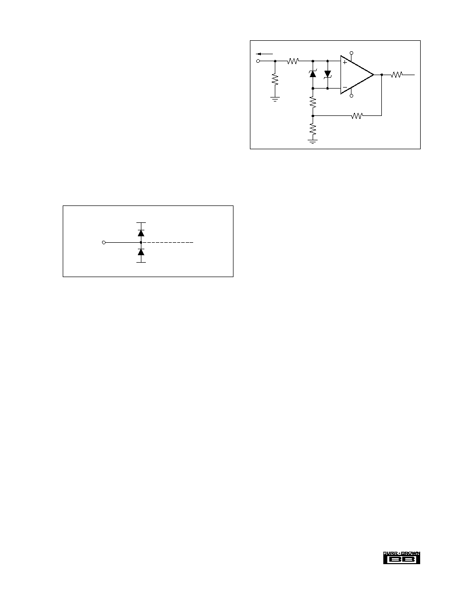
INPUT AND ESD PROTECTION
The OPA642 is built using a very high speed complemen-
tary bipolar process. The internal junction breakdown volt-
ages are relatively low due to these very small geometry
devices. These breakdowns are reflected in the Absolute
Maximum Rating table. All device pins are protected with
internal ESD protection diodes to the power supplies as
shown in Figure 9.
DESIGN-IN TOOLS
DEMONSTRATION BOARDS
Several PC boards are available in the initial evaluation of
circuit performance using the OPA642 in its three package
styles. Two partially assembled boards are available for sale
to support the DIP (P suffix) and SO-8 (U-suffix) packages.
These boards come partially assembled with power supply
and I/O connectors but do not have the amplifier or resistor
networks loaded. Both boards are configured for low
distortion, non-inverting amplifier operation. Order these
boards by the following part numbers from your local Burr-
Brown distributor:
DEM-OPA64XP-N for the OPA642P and OPA642PB (8-pin DIP package)
DEM-OPA64XU-N for the OPA642U and OPA642UB (8-pin SO package)
The SOT23-5 package version of the OPA642 may be
evaluated using a single unpopulated board used for numerous
SOT23-5 packaged amplifiers available from Burr-Brown.
This board is available from the Burr-Brown Literature
department as an unpopulated board attached to a descriptive
document. This board, the DEM-OPA6xxN, is available
free by requesting literature number MKT-348.
MACROMODELS AND APPLICATIONS SUPPORT
Computer simulation of circuit performance using SPICE is
often useful when analyzing the performance of analog
circuits and systems. This is particularly true for video and
RF amplifier circuits where parasitic capacitance and induc-
tance can have a major effect on circuit performance. A
SPICE model for the OPA642 is available through either the
Burr-Brown web page (http://www.burr-brown.com) or as a
disk from the Burr-Brown Applications Department (1-800-
548-6132). The application department is also available for
design assistance at this number. These models do a good
job of predicting small signal AC and transient performance
under a wide variety of operating conditions. They do not do
as good a job in predicting the harmonic distortion or dG/dP
characteristics. These models do not attempt to distinguish
between the package types in their small signal AC perfor-
mance.
These diodes provide moderate protection to input overdrive
voltages above the supplies as well. The protection diodes
can typically support 30mA continuous current. Where higher
currents are possible (e.g. in systems with
±
15V supply parts
driving into the OPA642), current limiting series resistors
should be added into the two inputs. Keep these resistor
values as low as possible since high values degrade both
noise performance and frequency response.
High input overdrive signals can also cause significant
differential voltage between the + and ≠ inputs. Where this
voltage can exceed the maximum rated voltage of
±
1.2V,
external Schottky protection diodes should be added across
the two inputs. Again, the capacitance added by these diodes
can degrade the noise and AC performance and should be
used only where necessary. Figure 9 shows a fully featured
input protection circuit for the OPA642. This is the circuit of
Figure 1 with additional limiting resistors into the inputs and
Schottky clamp diodes across the inputs. These resistor
values have been selected to limit the degradation in noise
and frequency response, achieve DC bias current cancella-
tion, and limit the current that will flow under overdrive
conditions.
External
Pin
+V
CC
≠V
CC
Internal
Circuitry
FIGURE 9. Internal ESD Protection.
301
50
Power Supply
Decoupling Not Shown
D1, D2
IN5911 (or equivalent)
301
50
50
D1
D2
50
Source
174
OPA642
+5V
≠5V
FIGURE 10. Gain of +2 with Input Protection.

PACKAGING INFORMATION
ORDERABLE DEVICE
STATUS(1)
PACKAGE TYPE
PACKAGE DRAWING
PINS
PACKAGE QTY
OPA642N/250
ACTIVE
SOP
DBV
5
250
OPA642N/3K
ACTIVE
SOP
DBV
5
3000
OPA642NB/250
OBSOLETE
SOP
DBV
5
OPA642NB/3K
OBSOLETE
SOP
DBV
5
OPA642P
OBSOLETE
PDIP
P
8
OPA642PB
OBSOLETE
PDIP
P
8
OPA642U
ACTIVE
SOIC
D
8
100
OPA642U/2K5
ACTIVE
SOIC
D
8
2500
OPA642UB
OBSOLETE
SOIC
D
8
OPA642UB/2K5
OBSOLETE
SOIC
D
8
(1) The marketing status values are defined as follows:
ACTIVE: Product device recommended for new designs.
LIFEBUY: TI has announced that the device will be discontinued, and a lifetime-buy period is in effect.
NRND: Not recommended for new designs. Device is in production to support existing customers, but TI does not recommend using this part in
a new design.
PREVIEW: Device has been announced but is not in production. Samples may or may not be available.
OBSOLETE: TI has discontinued the production of the device.
PACKAGE OPTION ADDENDUM
www.ti.com
3-Oct-2003

IMPORTANT NOTICE
Texas Instruments Incorporated and its subsidiaries (TI) reserve the right to make corrections, modifications,
enhancements, improvements, and other changes to its products and services at any time and to discontinue
any product or service without notice. Customers should obtain the latest relevant information before placing
orders and should verify that such information is current and complete. All products are sold subject to TI's terms
and conditions of sale supplied at the time of order acknowledgment.
TI warrants performance of its hardware products to the specifications applicable at the time of sale in
accordance with TI's standard warranty. Testing and other quality control techniques are used to the extent TI
deems necessary to support this warranty. Except where mandated by government requirements, testing of all
parameters of each product is not necessarily performed.
TI assumes no liability for applications assistance or customer product design. Customers are responsible for
their products and applications using TI components. To minimize the risks associated with customer products
and applications, customers should provide adequate design and operating safeguards.
TI does not warrant or represent that any license, either express or implied, is granted under any TI patent right,
copyright, mask work right, or other TI intellectual property right relating to any combination, machine, or process
in which TI products or services are used. Information published by TI regarding third-party products or services
does not constitute a license from TI to use such products or services or a warranty or endorsement thereof.
Use of such information may require a license from a third party under the patents or other intellectual property
of the third party, or a license from TI under the patents or other intellectual property of TI.
Reproduction of information in TI data books or data sheets is permissible only if reproduction is without
alteration and is accompanied by all associated warranties, conditions, limitations, and notices. Reproduction
of this information with alteration is an unfair and deceptive business practice. TI is not responsible or liable for
such altered documentation.
Resale of TI products or services with statements different from or beyond the parameters stated by TI for that
product or service voids all express and any implied warranties for the associated TI product or service and
is an unfair and deceptive business practice. TI is not responsible or liable for any such statements.
Following are URLs where you can obtain information on other Texas Instruments products and application
solutions:
Products
Applications
Amplifiers
amplifier.ti.com
Audio
www.ti.com/audio
Data Converters
dataconverter.ti.com
Automotive
www.ti.com/automotive
DSP
dsp.ti.com
Broadband
www.ti.com/broadband
Interface
interface.ti.com
Digital Control
www.ti.com/digitalcontrol
Logic
logic.ti.com
Military
www.ti.com/military
Power Mgmt
power.ti.com
Optical Networking
www.ti.com/opticalnetwork
Microcontrollers
microcontroller.ti.com
Security
www.ti.com/security
Telephony
www.ti.com/telephony
Video & Imaging
www.ti.com/video
Wireless
www.ti.com/wireless
Mailing Address:
Texas Instruments
Post Office Box 655303 Dallas, Texas 75265
Copyright
2003, Texas Instruments Incorporated