
OPA683
www.ti.com
Copyright © 2001, Texas Instruments Incorporated
Please be aware that an important notice concerning availability, standard warranty, and use in critical applications of
Texas Instruments semiconductor products and disclaimers thereto appears at the end of this data sheet.
SBOS221B ≠ NOVEMBER 2001 -- REVISED ≠ JUNE 2002
Very Low-Power, Current Feedback
OPERATIONAL AMPLIFIER With Disable
FEATURES
q
REDUCED BANDWIDTH CHANGE VERSUS GAIN
q
150MHz BANDWIDTH G = +2
q
> 90MHz BANDWIDTH TO GAIN > +10
q
LOW DISTORTION: < ≠69dBc at 5MHz
q
HIGH OUTPUT CURRENT: 110mA
q
SINGLE +5V TO +12V SUPPLY OPERATION
q
DUAL
±
2.5V TO
±
6V SUPPLY OPERATION
q
LOW SUPPLY CURRENT: 0.94mA
q
LOW SHUTDOWN CURRENT: 100
µ
A
V+
V
O
V≠
I
ERR
R
G
R
F
Patent Pending
Z
(S)
I
ERR
+
Low-Power
Amplifier
9
6
3
0
≠3
≠6
≠9
≠12
≠15
≠18
≠21
Normalized Gain (dB)
1
10
200
100
R
F
= 1.2k
Frequency (MHz)
OPA683 BANDWIDTH vs GAIN
G = 10
G = 20
G = 50
G = 100
G = 2
G = 5
DESCRIPTION
The OPA683 provides a new level of performance in very low-
power, wideband, current feedback amplifiers. This CFB
plus
ampli-
fier is among the first to use an internally closed-loop input buffer
stage that enhances performance significantly over earlier low-
power CFB amplifiers. While retaining the benefits of very low
power operation, this new architecture provides many of the
advantages of a more ideal CFB amplifier. The closed-loop input
stage buffer gives a very low and linearized impedance path at the
inverting input to sense the feedback error current. This improved
inverting input impedance gives exceptional bandwidth retention
to much higher gains and improved harmonic distortion over earlier
solutions limited by inverting input linearity. Beyond simple high
gain applications, the OPA683 CFB
plus
amplifier can allow the gain
setting element to be set with considerable freedom from amplifier
bandwidth interaction. This allows frequency response peaking
elements to be added, multiple input inverting summing circuits to
OPA6
83
OPA6
83
APPLICATIONS
q
LOW POWER BROADCAST VIDEO DRIVERS
q
EQUALIZING FILTERS
q
SAW FILTER HIGH GAIN POST AMPLIFIERS
q
SHORT LOOP ADSL CO DRIVERS
q
MULTICHANNEL SUMMING AMPLIFIERS
q
PROFESSIONAL CAMERAS
q
ADC INPUT DRIVERS
have greater bandwidth, and low-power line drivers to meet the
demanding requirements of studio cameras and broadcast video.
The output capability for the OPA683 also sets a new mark in
performance for very low-power current feedback amplifiers. De-
livering a full
±
4Vp-p swing on
±
5V supplies, the OPA683 also has
the output current to support this swing into a 100
load. This
minimal output headroom requirement is complemented by a
similar 1.2V input stage headroom giving exceptional capability for
single +5V operation.
The OPA683's low 0.94mA supply current is precisely trimmed at
25
∞
C. This trim, along with low shift over temperature and supply
voltage, gives a very robust design over a wide range of operating
conditions. System power may be further reduced by using the
optional disable control pin. Leaving this disable pin open, or holding
it HIGH, gives normal operation. If pulled LOW, the OPA683 supply
current drops to less than 100
µ
A while the I/O pins go to a high
impedance state.
PRODUCTION DATA information is current as of publication date.
Products conform to specifications per the terms of Texas Instruments
standard warranty. Production processing does not necessarily include
testing of all parameters.

OPA683
2
SBOS221B
www.ti.com
ABSOLUTE MAXIMUM RATINGS
(1)
Power Supply ...............................................................................
±
6.5V
DC
Internal Power Dissipation ................................. See Thermal Information
Differential Input Voltage ..................................................................
±
1.2V
Input Voltage Range ............................................................................
±
V
S
Storage Temperature Range: ID, IDBV ......................... ≠40
∞
C to +125
∞
C
Lead Temperature (soldering, 10s) .............................................. +300
∞
C
Junction Temperature (T
J
) ........................................................... +175
∞
C
NOTE: (1) Stresses above those listed under "Absolute Maximum Ratings"
may cause permanent damage to the device. Exposure to absolute maximum
conditions for extended periods may affect device reliability.
SPECIFIED
PACKAGE
TEMPERATURE
PACKAGE
ORDERING
TRANSPORT
PRODUCT
PACKAGE-LEAD
DESIGNATOR
(1)
RANGE
MARKING
NUMBER
MEDIA, QUANTITY
OPA683
SO-8
D
≠40
∞
C to +85
∞
C
OPA683D
OPA683ID
Rails,100
"
"
"
"
"
OPA683IDR
Tape and Reel, 2500
OPA683
SOT23-6
DBV
≠40
∞
C to +85
∞
C
A83
OPA683IDBVT
Tape and Reel, 250
"
"
"
"
"
OPA683IDBVR
Tape and Reel, 3000
PACKAGE/ORDERING INFORMATION
ELECTROSTATIC
DISCHARGE SENSITIVITY
This integrated circuit can be damaged by ESD. Texas Instru-
ments recommends that all integrated circuits be handled with
appropriate precautions. Failure to observe proper handling
and installation procedures can cause damage.
ESD damage can range from subtle performance degradation to
complete device failure. Precision integrated circuits may be more
susceptible to damage because very small parametric changes
could cause the device not to meet its published specifications.
1
2
3
6
5
4
Output
≠V
S
Noninverting Input
+V
S
DIS
Inverting Input
1
2
3
6
5
4
A83
Pin Orientation/Package Marking
1
2
3
4
8
7
6
5
NC
Inverting Input
Noninverting Input
≠V
S
DIS
+V
S
Output
NC
NC = No Connection
PIN CONFIGURATION
OPA683 RELATED PRODUCTS
SINGLES
DUALS
TRIPLES
QUADS
FEATURES
OPA684
OPA2683
OPA3684
OPA4684
Low-Power CFB
plus
OPA691
OPA2691
OPA3691
--
High Slew Rate CFB
OPA685
--
--
--
> 500MHz CFB
Top View
SO-8
Top View
SOT23-6
NOTES: (1) For the most current specifications, and package information, refer to our web site at www.ti.com.

OPA683
3
SBOS221B
www.ti.com
AC PERFORMANCE (See Figure 1)
Small-Signal Bandwidth (V
O
= 0.5Vp-p)
G = +1, R
F
= 1.2k
200
MHz
typ
C
G = +2, R
F
= 1.2k
150
124
121
117
MHz
min
B
G = +5, R
F
= 1.2k
121
MHz
typ
C
G = +10, R
F
= 1.2k
94
MHz
typ
B
G = +20, R
F
= 1.2k
72
MHz
typ
C
Bandwidth for 0.1dB Gain Flatness
G = +2, V
O
= 0.5Vp-p, R
F
= 1.2k
37
15
14
14
MHz
min
B
Peaking at a Gain of +1
R
F
= 1.2k
, V
O
= 0.5Vp-p
1.8
6.5
7.7
8.0
dB
max
B
Large-Signal Bandwidth
G = +2, V
O
= 4Vp-p
63
MHz
typ
C
Slew Rate
G = ≠1, V
O
= 4V Step (see Figure 2)
540
450
450
430
V/
µ
s
min
B
G = +2,V
O
= 4V Step
400
345
338
336
V/
µ
s
min
B
Rise-and-Fall Time
G = +2, V
O
= 0.5V Step
4.6
ns
typ
C
G = +2, V
O
= 4VStep
7.8
ns
typ
C
Harmonic Distortion
G = +2, f = 5MHz, V
O
= 2Vp-p
2nd-Harmonic
R
L
= 100
≠63
≠54
≠54
≠54
dBc
max
B
R
L
1k
≠65
≠55
≠55
≠55
dBc
max
B
3rd-Harmonic
R
L
= 100
≠67
≠62
≠62
≠62
dBc
max
B
R
L
1k
≠74
≠67
≠66
≠66
dBc
max
B
Input Voltage Noise
f > 1MHz
4.4
5.0
5.5
5.8
nV/
Hz
max
B
Noninverting Input Current Noise
f > 1MHz
5.1
5.8
6.4
6.7
pA/
Hz
max
B
Inverting Input Current Noise
f > 1MHz
11.6
11.9
12.3
12.4
pA/
Hz
max
B
Differential Gain
G = +2, NTSC, V
O
= 1.4Vp, R
L
= 150
0.06
%
typ
C
Differential Phase
G = +2, NTSC, V
O
= 1.4Vp, R
L
= 150
0.03
deg
typ
C
DC PERFORMANCE
(4)
Open-Loop Transimpedance Gain (Z
OL
)
V
O
= 0V, R
L
= 1k
700
360
270
250
k
min
A
Input Offset Voltage
V
CM
= 0V
±
1.5
±
3.5
±
4.1
±
4.3
mV
max
A
Average Offset Voltage Drift
V
CM
= 0V
±
12
±
12
µ
V/
∞
C
max
B
Noninverting Input Bias Current
V
CM
= 0V
±
2.0
±
4.0
±
4.6
±
4.8
µ
A
max
A
Average Noninverting Input Bias Current Drift
V
CM
= 0V
±
15
±
15
nA/
∞
C
max
B
Inverting Input Bias Current
V
CM
= 0V
±
3.0
±
10
±
11
±
11.5
µ
A
max
A
Average Inverting Input Bias Current Drift
V
CM
= 0V
±
20
±
20
nA
∞
/C
max
B
INPUT
Common-Mode Input Range
(5)
(CMIR)
±
3.75
±
3.65
±
3.65
±
3.60
V
min
A
Common-Mode Rejection Ratio (CMRR)
V
CM
= 0V
60
53
52
52
dB
min
A
Noninverting Input Impedance
50
2
k
|| pF
typ
C
Inverting Input Resistance (R
I
)
Open-Loop, DC
4.5
typ
C
OUTPUT
Voltage Output Swing
1k
Load
±
4.1
±
4.0
±
4.0
±
3.9
V
min
A
Current Output, Sourcing
V
O
= 0
150
130
125
120
mA
min
A
Current Output, Sinking
V
O
= 0
≠110
≠100
≠95
≠90
mA
min
A
Closed-Loop Output Impedance
G = +2, f = 100kHz
0.007
typ
C
DISABLE (Disabled LOW)
Power-Down Supply Current (+V
S
)
V
DIS
= 0
≠100
≠150
≠170
≠180
µ
A
typ
C
Disable Time
V
IN
= +1, See Figure 1
60
ms
typ
C
Enable Time
V
IN
= +1, See Figure 1
40
ns
typ
C
Off Isolation
G = +2, 5MHz
70
dB
typ
C
Output Capacitance in Disable
1.7
pF
typ
C
Turn On Glitch
G = +2, R
L
= 150
, V
IN
= 0
±
70
mV
typ
C
Turn Off Glitch
G = +2, R
L
= 150
, V
IN
= 0
±
20
mV
typ
C
Enable Voltage
3.4
3.5
3.6
3.7
V
min
A
Disable Voltage
1.8
1.7
1.6
1.5
V
max
A
Control Pin Input Bias Current (DIS)
V
DIS
= 0V
80
120
130
135
µ
A
max
A
POWER SUPPLY
Specified Operating Voltage
±
5
V
typ
C
Maximum Operating Voltage Range
±
6
±
6
±
6
V
max
A
Max Quiescent Current
V
S
=
±
5V
0.94
1.03
1.04
1.05
mA
max
A
Min Quiescent Current
V
S
=
±
5V
0.94
0.85
0.80
0.77
mA
min
A
Power-Supply Rejection Ratio (≠PSRR)
Input Referred
62
55
54
54
dB
typ
A
TEMPERATURE RANGE
Specification: D, DBV
≠40 to +85
∞
C
typ
C
Thermal Resistance,
JA
Junction-to-Ambient
D
SO-8
125
∞
C/W
typ
C
DBV SOT-23-6
150
∞
C/W
typ
C
NOTES: (1) Junction temperature = ambient for 25
∞
C tested specifications. (2) Junction temperature = ambient at low temperature limit: junction temperature = ambient
+2
∞
C at high temperature limit for over temperature tested specifications. (3) Test levels: (A) 100% tested at 25
∞
C. Over temperature limits by characterization and
simulation. (B) Limits set by characterization and simulation. (C) Typical value only for information. (4) Current is considered positive out-of-node. V
CM
is the input
common-mode voltage. (5) Tested < 3dB below minimum specified CMR at
±
CMIR limits.
ELECTRICAL CHARACTERISTICS: V
S
=
±
5V
R
F
= 1.2k
, R
L
= 1k
, and G = +2
,
(see Figure 1 for AC performance only), unless otherwise noted.
OPA683ID, IDBV
TYP
MIN/MAX OVER TEMPERATURE
0
∞
C to
≠40
∞
C to
MIN/
TEST
PARAMETER
CONDITIONS
+25
∞
C
+25
∞
C
(1)
70
∞
C
(2)
+85
∞
C
(2)
UNITS
MAX
LEVEL
(3)

OPA683
4
SBOS221B
www.ti.com
AC PERFORMANCE (See Figure 3)
Small-Signal Bandwidth (V
O
= 0.2Vp-p)
G = +1, R
F
= 1.4k
145
MHz
typ
G = +2, R
F
= 1.4k
119
96
92
90
MHz
min
B
G = +5, R
F
= 1.4k
95
MHz
typ
C
G = +10, R
F
= 1.4k
87
MHz
typ
C
G = +20, R
F
= 1.4k
60
MHz
typ
C
Bandwidth for 0.1dB Gain Flatness
G = +2, V
O
< 0.5Vp-p, R
F
= 1.2k
14
9
8
8
MHz
min
B
Peaking at a Gain of +1
R
F
= 1.4k
, V
O
< 0.5Vp-p
1
6
8
8
dB
max
B
Large-Signal Bandwidth
G = +2, V
O
= 2Vp-p
70
MHz
typ
C
Slew Rate
G = +2, V
O
= 2V Step
210
180
175
170
V/
µ
s
min
B
Rise-and-Fall Time
G = +2, V
O
= 0.5V Step
5.9
ns
typ
C
G = +2, V
O
= 2VStep
7.8
ns
typ
C
Harmonic Distortion
G = 2, f = 5MHz, V
O
= 2Vp-p
2nd-Harmonic
R
L
= 100
to V
S
/2
≠60
≠54
≠53
≠53
dBc
max
B
R
L
1k
to V
S
/2
≠66
≠55
≠55
≠55
dBc
max
B
3rd-Harmonic
R
L
= 100
to V
S
/2
≠59
≠58
≠58
≠58
dBc
max
B
R
L
1k
to V
S
/2
≠63
≠57
≠56
≠56
dBc
max
B
Input Voltage Noise
f > 1MHz
4.4
5.0
5.5
5.8
nV/
Hz
max
B
Noninverting Input Current Noise
f > 1MHz
5.1
5.8
6.4
6.7
pA/
Hz
max
B
Inverting Input Current Noise
f > 1MHz
11.6
11.9
12.3
12.4
pA/
Hz
max
B
Differential Gain
G = +2, NTSC, V
O
= 1.4Vp, R
L
= 150
0.24
%
typ
C
Differential Phase
G = +2, NTSC, V
O
= 1.4Vp, R
L
= 150
0.19
deg
typ
C
DC PERFORMANCE
(4)
Open-Loop Transimpedance Gain (Z
OL
)
V
O
= V
S
/2, R
L
= 1k
to V
S
/2
700
300
270
250
k
min
A
Input Offset Voltage
V
CM
= V
S
/2
±
1.0
±
3.0
±
3.6
±
3.8
mV
max
A
Average Offset Voltage Drift
V
CM
= V
S
/2
±
12
±
12
µ
V/
∞
C
max
B
Noninverting Input Bias Current
V
CM
= V
S
/2
±
2
±
4
±
4.6
±
4.8
µ
A
max
A
Average Noninverting Input Bias Current Drift
V
CM
= V
S
/2
±
12
±
12
nA/
∞
C
max
B
Inverting Input Bias Current
V
CM
= V
S
/2
±
3
±
8
±
8.7
±
8.9
µ
A
max
A
Average Inverting Input Bias Current Drift
V
CM
= V
S
/2
±
15
±
15
nA
∞
/C
max
B
INPUT
Least Positive Input Voltage
(5)
1.1
1.25
1.29
1.34
V
max
A
Most Positive Input Voltage
(5)
3.9
3.75
3.73
3.67
V
min
A
Common-Mode Refection Ratio (CMRR)
V
CM
= V
S
/2
58
51
50
50
dB
min
A
Noninverting Input Impedance
50
2
k
|| pF
typ
C
Inverting Input Resistance (R
I
)
Open-Loop
4.8
typ
C
OUTPUT
Most Positive Output Voltage
R
L
= 1k
to V
S
/2
4.2
4.1
4.1
4.0
V
min
A
Least Positive Output Voltage
R
L
= 1k
to V
S
/2
0.8
0.9
0.9
1.00
min
A
Current Output, Sourcing
V
O
= V
S
/2
80
65
63
58
mA
min
A
Current Output, Sinking
V
O
= V
S
/2
70
52
50
45
mA
min
A
Closed-Loop Output Impedance
G = +2, f = 100kHz
0.009
typ
C
DISABLE (Disabled LOW)
Power-Down Supply Current (+V
S
)
V
DIS
= 0
100
µ
A
typ
C
Off Isolation
G = +2, 5MHz
70
dB
typ
C
Output Capacitance in Disable
1.7
pF
typ
C
Turn On Glitch
G = +2, R
L
= 150
, V
IN
= V
S
/2
±
70
mV
typ
C
Turn Off Glitch
G = +2, R
L
= 150
, V
IN
= V
S
/2
±
20
mV
typ
C
Enable Voltage
3.4
3.5
3.6
3.7
V
min
A
Disable Voltage
1.8
1.7
1.6
1.5
V
max
A
Control Pin Input Bias Current (DIS)
V
DIS
= 0V
80
120
130
135
µ
A
max
A
POWER SUPPLY
Specified Single-Supply Operating Voltage
5
V
typ
C
Max Single-Supply Operating Voltage
12
12
12
V
max
A
Max Quiescent Current
V
S
= +5V
0.82
0.91
0.91
0.91
mA
max
A
Min Quiescent Current
V
S
= +5V
0.82
0.71
0.69
0.67
mA
min
A
Power-Supply Rejection Ratio (+PSRR)
Input Referred
65
dB
typ
C
TEMPERATURE RANGE
Specification: D, DBV
≠40 to +85
∞
C
typ
C
Thermal Resistance,
JA
Junction-to-Ambient
D
SO-8
125
∞
C/W
typ
C
DBV SOT-23-6
150
∞
C/W
typ
C
NOTES: (1) Junction temperature = ambient for 25
∞
C tested specifications. (2) Junction temperature = ambient at low temperature limit: junction temperature = ambient
+2
∞
C at high temperature limit for over temperature tested specifications. (3) Test levels: (A) 100% tested at 25
∞
C. Over temperature limits by characterization and
simulation. (B) Limits set by characterization and simulation. (C) Typical value only for information. (4) Current is considered positive out-of-node. V
CM
is the input
common-mode voltage. (5) Tested < 3dB below minimum specified CMR at
±
CMIR limits.
ELECTRICAL CHARACTERISTICS: V
S
= +5V
R
F
= 1.4k
, R
L
= 1k
, and G = +2
,
(see Figure 3 for AC performance only), unless otherwise noted.
OPA683ID, IDBV
TYP
MIN/MAX OVER TEMPERATURE
0
∞
C to
≠40
∞
C to
MIN/
TEST
PARAMETER
CONDITIONS
+25
∞
C
+25
∞
C
(1)
70
∞
C
(2)
+85
∞
C
(2)
UNITS
MAX
LEVEL
(3)

OPA683
5
SBOS221B
www.ti.com
TYPICAL CHARACTERISTICS: V
S
=
±
5V
T
A
= 25
∞
C, R
F
= 1.2k
, R
L
= 1k
, and G = +2
,
(see Figure 1 for AC performance only), unless otherwise noted.
INVERTING PULSE RESPONSE
Time (10ns/div)
Output V
oltage (200mV/div)
Output V
oltage (800mV/div)
0.8
0.6
0.4
0.2
0
≠0.2
≠0.4
≠0.6
≠0.8
3.2
2.4
1.6
0.8
0
≠0.8
≠1.6
≠2.4
≠3.2
Large-Signal Right Scale
Small-Signal Left Scale
See Figure 2
G = ≠1
9
6
3
0
≠3
Frequency (MHz)
1
200
10
100
NONINVERTING LARGE-SIGNAL
FREQUENCY RESPONSE
Gain (dB)
G = +2
R
L
= 1k
See Figure 1
V
O
= 0.5Vp-p
V
O
= 1Vp-p
V
O
= 5Vp-p
V
O
= 2Vp-p
3
0
≠3
≠6
≠9
≠12
Frequency (MHz)
1
200
10
100
INVERTING LARGE-SIGNAL FREQUENCY RESPONSE
Gain (dB)
G = ≠1
R
L
= 1k
V
O
= 0.5Vp-p
See Figure 2
V
O
= 2Vp-p
V
O
= 1Vp-p
V
O
= 5Vp-p
NONINVERTING PULSE RESPONSE
Time (10ns/div)
Output V
oltage (200mV/div)
Output V
oltage (800mV/div)
0.8
0.6
0.4
0.2
0
≠0.2
≠0.4
≠0.6
≠0.8
3.2
2.4
1.6
0.8
0
≠0.8
≠1.6
≠2.4
≠3.2
Large-Signal Right Scale
Small-Signal Left Scale
See Figure 1
G = +2
6
3
0
≠3
≠6
≠9
≠12
Frequency (MHz)
1
200
10
100
NONINVERTING SMALL-SIGNAL
FREQUENCY RESPONSE
Normalized Gain (3dB/div)
V
O
= 0.5Vp-p
R
F
= 1.2k
G = 100
See Figure 1
G = 50
G = 10
G = 1
G = 2
G = 5
3
0
≠3
≠6
≠9
≠12
Frequency (MHz)
1
200
10
100
INVERTING SMALL-SIGNAL FREQUENCY RESPONSE
Normalized Gain (3dB/div)
V
O
= 0.5Vp-p
R
F
= 1.2k
See Figure 2
G = ≠10
G = ≠24
G = ≠5
G = ≠1
G = ≠2

OPA683
6
SBOS221B
www.ti.com
TYPICAL CHARACTERISTICS: V
S
=
±
5V
(Cont.)
T
A
= 25
∞
C, R
F
= 1.2k
, R
L
= 1k
, and G = +2
,
(see Figure 1 for AC performance only), unless otherwise noted.
HARMONIC DISTORTION vs LOAD RESISTANCE
100
1k
Load Resistance (
)
Harmonic Distortion (dBc)
≠50
≠55
≠60
≠65
≠70
≠75
≠80
≠85
≠90
V
O
= 2Vp-p
f = 5MHz
G = +2
See Figure 1
2nd-Harmonic
3rd-Harmonic
≠50
≠60
≠70
≠80
≠90
Frequency (MHz)
0.1
20
1
10
HARMONIC DISTORTION vs FREQUENCY
Harmonic Distortion (dBc)
V
O
= 2Vp-p
R
L
= 1k
See Figure 1
2nd-Harmonic
3rd-Harmonic
HARMONIC DISTORTION vs OUTPUT VOLTAGE
0.5
1
5
Output Voltage (Vp-p)
Harmonic Distortion (dBc)
≠50
≠60
≠70
≠80
≠90
f = 5MHz
R
L
= 1k
2nd-Harmonic
3rd-Harmonic
See Figure 1
HARMONIC DISTORTION vs NONINVERTING GAIN
Gain (V/V)
Harmonic Distortion (dBc)
See Figure 1
1
10
20
≠50
≠55
≠60
≠65
≠70
≠75
≠80
≠85
≠90
V
O
= 2Vp-p
f = 5MHz
R
L
= 1k
2nd-Harmonic
3rd-Harmonic
HARMONIC DISTORTION vs INVERTING GAIN
1
10
20
Inverting Gain (≠V/V)
Harmonic Distortion (dBc)
≠50
≠55
≠60
≠65
≠70
≠75
≠80
≠85
≠90
3rd-Harmonic
2nd-Harmonic
V
O
= 2Vp-p
f = 5MHz
R
L
= 1k
See Figure 2
5MHz HARMONIC DISTORTION vs SUPPLY VOLTAGE
±
2.5
±
3
±
3.5
±
4
±
4.5
±
5
±
5.5
±
6
Supply Voltage (
±
V)
Harmonic Distortion (dBc)
≠50
≠60
≠70
≠80
≠90
V
O
= 2Vp-p
R
L
= 1k
2nd-Harmonic
3rd-Harmonic
See Figure 1

OPA683
7
SBOS221B
www.ti.com
TYPICAL CHARACTERISTICS: V
S
=
±
5V
(Cont.)
T
A
= 25
∞
C, R
F
= 1.2k
, R
L
= 1k
, and G = +2
,
(see Figure 1 for AC performance only), unless otherwise noted.
100
10
1
Frequency (Hz)
10
2
10
7
10
3
10
4
10
5
10
6
INPUT VOLTAGE AND CURRENT NOISE DENSITY
Voltage Noise (nV/
Hz)
Current Noise (pA/
Hz)
Noninverting Current Noise
5.2pA/
Hz
Voltage Noise
4.4nV/
Hz
Inverting Current Noise
11.6pA/
Hz
160
140
120
100
80
60
40
20
0
C
LOAD
(pF)
1
100
10
R
S
vs C
LOAD
R
S
(
)
0.5dB Peaking
2-TONE, 3RD-ORDER
INTERMODULATION DISTORTION
Vp-p at 1k
Load (each tone)
3rd-Order Spurious Level (dBc)
≠45
≠55
≠65
≠75
≠85
1MHz
20MHz
0.1
0.4
1
2
5MHz
10MHz
+5V
≠5V
50
1k
P
I
P
O
1.2k
1.2k
OPA684
6
5
4
3
2
1
0
Time (ms)
0
100
10
20
40
30
80
70
90
60
50
DISABLE TIME
V
DIS
V
OUT
V
OUT
and V
DIS
(V)
V
IN
=
1V
DC
See Figure 1
≠40
≠50
≠60
≠70
≠80
≠90
≠100
Frequency (MHz)
0.1
100
1
10
DISABLED FEEDTHRU
Feedthru (dB)
G = +2
V
DIS
= 0V
See Figure 1
9
6
3
0
≠3
≠6
Frequency (MHz)
1
200
10
100
SMALL-SIGNAL BANDWIDTH vs C
LOAD
Normalized Gain (dB)
10pF
100pF
47pF
22pF
R
S
V
O
+5V
≠5V
50
C
L
V
I
1.2k
1.2k
1k
OPA683

OPA683
8
SBOS221B
www.ti.com
TYPICAL CHARACTERISTICS: V
S
=
±
5V
(Cont.)
T
A
= 25
∞
C, R
F
= 1.2k
, R
L
= 1k
, and G = +2
,
(see Figure 1 for AC performance only), unless otherwise noted.
CMRR and PSRR vs FREQUENCY
10
2
10
3
10
4
10
5
10
6
10
7
10
8
Frequency (Hz)
Common-Mode Rejection Ratio (dB)
Power-Supply Rejection Ratio (dB)
70
60
50
40
30
20
10
0
CMRR
+PSRR
≠PSRR
OPEN-LOOP TRANSIMPEDANCE GAIN AND PHASE
10
4
10
5
10
6
10
7
10
8
10
9
Frequency (Hz)
Open-Loop
T
ransimpedance Gain (dB
) 120
100
80
60
40
20
0
Open-Loop Phase (
∞
)
0
≠30
≠60
≠90
≠120
≠150
≠180
20log (Z
OL
)
Z
OL
0.2
0.15
0.1
0.05
0
Number of 150
Video Loads
1
4
2
3
COMPOSITE VIDEO DIFFERENTIAL GAIN/PHASE
Differential Gain (%)
Differential Phase (
∞
)
Gain = +2
NTSC, Positive Video
dG
dP
TYPICAL DC DRIFT OVER TEMPERATURE
≠50
≠25
0
25
50
75
100
125
Ambient Temperature (
∞
C)
Input Bias Currents (
µ
A)
and Of
fset V
oltage (mV)
4
3
2
1
0
≠1
≠2
≠3
≠4
Input Offset Voltage
Noninverting Input Bias Current
Inverting Input Bias Current
OUTPUT CURRENT AND VOLTAGE LIMITATIONS
≠150
≠100
≠50
0
50
100
150
I
O
(mA)
V
O
(V)
5
4
3
2
1
0
≠1
≠2
≠3
≠4
≠5
1W Power
Limit
R
L
= 100
R
L
=
5
0
R
L
= 500
1W Power
Limit
SUPPLY AND OUTPUT CURRENT
vs TEMPERATURE
≠25
0
25
50
75
100
125
Ambient Temperature (
∞
C)
Output Current (mA)
200
175
150
125
100
1
0.95
0.9
0.85
0.8
Supply Current (mA)
Sourcing Output Current
Sinking Output Current
Supply Current
Right Scale

OPA683
9
SBOS221B
www.ti.com
TYPICAL CHARACTERISTICS: V
S
=
±
5V
(Cont.)
T
A
= 25
∞
C, R
F
= 1.2k
, R
L
= 1k
, and G = +2
,
(see Figure 1 for AC performance only), unless otherwise noted.
SETTLING TIME
0
10
20
30
40
50
60
Time (ns)
% Error to Final V
alue
0.05
0.04
0.03
0.02
0.01
0
≠0.01
≠0.02
≠0.03
≠0.04
≠0.05
2V Step
See Figure 1
DISABLED SUPPLY CURRENT vs TEMPERATURE
≠50
≠25
25
0
50
75
100
125
Ambient Temperature (
∞
C)
Disabled Supply Current (
µ
A)
110
100
90
80
70
60
+V
S
Current
NONINVERTING OVERDRIVE RECOVERY
Time (100ns/div)
Input V
oltage (0.8V/div)
Output V
oltage (1.6V/div)
4.0
3.2
2.4
1.6
0.8
0
≠0.8
≠1.6
≠2.4
≠3.2
≠4.0
8.0
6.4
4.8
3.2
1.6
0
≠1.6
≠3.2
≠4.8
≠6.4
≠8.0
See Figure 1
Input Voltage
Left Scale
Output Voltage
Right Scale
INPUT AND OUTPUT RANGE vs SUPPLY VOLTAGE
±
Supply Voltage
±
4
±
3
±
2
±
5
±
6
Input and Output V
oltage Range
6
5
4
3
2
1
0
≠1
≠2
≠3
≠4
≠5
≠6
Input
Voltage
Range
Output
Voltage
Range
CLOSED-LOOP OUTPUT IMPEDANCE vs FREQUENCY
Frequency (Hz)
100k
1M
1k
10k
100
10M
100M
Output Impedance (
)
100
10
1
0.01
0.001
1.2k
Z
O
1.2k
OPA683
INVERTING OVERDRIVE RECOVERY
Time (100ns/div)
Input V
oltage (1.6V/div)
Input V
oltage (1.6V/div)
8.0
6.4
4.8
3.2
1.6
0
≠1.6
≠3.2
≠4.8
≠6.4
≠8.0
8.0
6.4
4.8
3.2
1.6
0
≠1.6
≠3.2
≠4.8
≠6.4
≠8.0
Input Voltage
Left Scale
See Figure 2
Output Voltage
Right Scale

OPA683
10
SBOS221B
www.ti.com
TYPICAL CHARACTERISTICS: V
S
= +5V
T
A
= 25
∞
C, R
F
= 1.4k
, R
L
= 1k
, and G = +2
,
(see Figure 3 for AC performance only), unless otherwise noted.
6
3
0
≠3
≠6
≠9
≠12
≠15
≠18
Frequency (MHz)
1
200
10
100
NONINVERTING SMALL-SIGNAL
FREQUENCY RESPONSE
Normalized Gain (dB)
See Figure 3
G = 50
R
F
= 1.4k
V
O
= 0.2Vp-p
R
L
= 1k
G = 1
G = 2
G = 20
G = 10
G = 5
3
0
≠3
≠6
≠9
≠12
Frequency (MHz)
1
200
10
100
INVERTING LARGE-SIGNAL FREQUENCY RESPONSE
Gain (dB)
V
O
= 0.2Vp-p
See Figure 4
V
O
= 1Vp-p
V
O
= 0.5Vp-p
V
O
= 2Vp-p
G = ≠1
R
L
= 1k
9
6
3
0
≠3
Frequency (MHz)
1
200
10
100
NONINVERTING LARGE-SIGNAL
FREQUENCY RESPONSE
Gain (dB)
0.5Vp-p
1Vp-p
0.2Vp-p
2Vp-p
See Figure 3
G = +2
R
L
= 1k
3
0
≠3
≠6
≠9
≠12
Frequency (MHz)
1
200
10
100
INVERTING SMALL-SIGNAL FREQUENCY RESPONSE
Normalized Gain (3dB/div)
See Figure 4
R
F
= 1.4k
V
O
= 0.2Vp-p
R
L
= 1k
G = ≠1
G = ≠10
G = ≠28
G = ≠5
G = ≠2
NONINVERTING PULSE RESPONSE
Time (10ns/div)
Output V
oltage (100mV/div)
Output V
oltage (400mV/div)
0.4
0.3
0.2
0.1
0
≠0.1
≠0.2
≠0.3
≠0.4
1.6
1.2
0.8
0.4
0
≠0.4
≠0.8
≠1.2
≠1.6
Large-Signal Right Scale
Small-Signal Left Scale
See Figure 3
INVERTING PULSE RESPONSE
Time (10ns/div)
Output V
oltage (100mV/div)
Output V
oltage (400mV/div)
0.4
0.3
0.2
0.1
0
≠0.1
≠0.2
≠0.3
≠0.4
1.6
1.2
0.8
0.4
0
≠0.4
≠0.8
≠1.2
≠1.6
Large-Signal Right Scale
Small-Signal Left Scale
See Figure 4

OPA683
11
SBOS221B
www.ti.com
TYPICAL CHARACTERISTICS: V
S
= +5V
(Cont.)
T
A
= 25
∞
C, R
F
= 1.4k
, R
L
= 1k
, and G = +2
,
(see Figure 3 for AC performance only), unless otherwise noted.
HARMONIC DISTORTION vs LOAD RESISTANCE
100
1k
Load Resistance (
)
Harmonic Distortion (dBc)
≠50
≠55
≠60
≠65
≠70
≠75
≠80
≠85
≠90
V
O
= 2Vp-p
f = 5MHz
See Figure 3
3rd-Harmonic
2nd-Harmonic
≠50
≠60
≠70
≠80
≠90
Frequency (MHz)
0.1
20
1
10
HARMONIC DISTORTION vs FREQUENCY
Harmonic Distortion (dBc)
V
O
= 2Vp-p
R
L
= 1k
See Figure 3
2nd-Harmonic
3rd-Harmonic
≠50
≠60
≠70
≠80
≠90
Output Voltage (Vp-p)
0.5
3
1
2
HARMONIC DISTORTION vs OUTPUT VOLTAGE
Harmonic Distortion (dBc)
3rd-Harmonic
2nd-Harmonic
See Figure 3
G = +2
R
L
= 1k
f = 5MHz
0.3
0.25
0.2
0.15
0.1
0.05
0
Number of 150
Video Loads
1
4
2
3
COMPOSITE VIDEO DIFFERENTIAL GAIN/PHASE
Differential Gain (%)
Differential Phase (
∞
)
dP
dG
G = +2
NTSC, Positive Video
2-TONE, 3RD-ORDER
INTERMODULATION DISTORTION
0.1
1
Vp-p at 1
Load (each tone)
3rd-Order Spurious Level (dBc)
≠45
≠55
≠65
≠75
≠85
See Figure 3
10MHz
20MHz
5MHz
SUPPLY AND OUTPUT CURRENT
vs TEMPERATURE
≠50
≠25
0
25
50
100
75
125
Ambient Temperature (
∞
C)
Output Current (mA)
100
90
80
70
60
50
0.95
0.9
0.85
0.8
0.75
0.7
Supply Current (mA)
Left Scale
Sinking Output Current
Right Scale
Supply Current
Sourcing Output Current
Left Scale

OPA683
12
SBOS221B
www.ti.com
APPLICATIONS INFORMATION
VERY LOW POWER CURRENT-FEEDBACK
OPERATION
The OPA683 gives a new level of performance in very low
power current-feedback op amps. Using a new input stage
buffer architecture, the OPA683 CFB
plus
amplifier gives im-
proved bandwidth to higher gains than previous < 1mA
supply current amplifiers. This closed-loop internal buffer
gives a very low and linearized impedance at the inverting
node--isolating the amplifier's AC performance from gain
element variations. This allows both the bandwidth and
distortion to remain nearly constant over gain--moving closer
to the ideal current-feedback performance of Gain Bandwidth
independence. This low power amplifier also delivers excep-
tional output power--it's
±
4V swing on
±
5V supplies with
> 100mA output drive gives excellent performance into
standard video loads or doubly-terminated 50
cables. Single
+5V supply operation is also supported with similar band-
widths, but reduced output power capability. For improved
harmonic distortion driving heavier loads, in a low power
CFB
plus
amplifier, consider the OPA684 while, for even
higher output power, consider the OPA691.
Figure 1 shows the DC-coupled, gain of +2, dual power-
supply circuit used as the basis of the
±
5V Electrical Charac-
teristics and Typical Characteristics. For test purposes, the
input impedance is set to 50
with a resistor to ground while
the output load is a 1k
resistor. Voltage swings reported in
the specifications are taken directly at the input and output
pins while load powers (dBm) are interpreted as the voltage
swing at the output converted to dBm as if the load were
50
. For the circuit of Figure 1, the total effective load will be
1k
|| 2.4k
= 706
. Gain changes are most easily accom-
plished by simply resetting the R
G
value--holding R
F
con-
stant at its recommended value of 1.2k
. The disable control
line (DIS) is typically left open to ensure normal amplifier
operation. It may, however, be asserted LOW to reduce the
amplifier quiescent to 100
µ
A typically.
Figure 2 shows the DC-coupled, gain of ≠1V/V, dual power-
supply circuit used as the basis of the Inverting Typical
Characteristics. Inverting operation offers several perfor-
mance benefits. Since there is no common-mode signal
across the input stage, the slew rate for inverting operation
is higher and the distortion performance is slightly improved.
An additional input resistor, R
M
, is included in Figure 2 to set
the input impedance equal to the 50
. The parallel combina-
tion of R
M
and R
G
set the input impedance. As the desired
gain increases for the inverting configuration, R
G
is adjusted
to achieved the desired gain and R
M
is also adjusted to hold
a 50
input match. A point will be reached where R
G
will
equal 50
, R
M
is then removed and the input match is set by
R
G
only. With R
G
fixed to achieve an input match to 50
, to
increase gain, R
F
is simply increased. This will, however,
quickly reduce the achievable bandwidth as the feedback
resistor increases from its recommended value of 1.2k
. If
the source does not require an input match to 50
, either
adjust R
M
to the get the desired load or remove it and let the
R
G
resistor alone provide the input load.
R
F
1.2k
V
O
OPA683
+5V
≠5V
DIS
1k
50
R
G
1.2k
R
G
=
50
V
I
0.1
µ
F
6.8
µ
F
0.1
µ
F
6.8
µ
F
+
+
FIGURE 1. DC-Coupled, G = +2V/V, Bipolar Supply, Speci-
fication and Test Circuit.
FIGURE 2. DC-Coupled, G = ≠1V/V, Bipolar Supply, Speci-
fication and Test Circuit.
R
F
1.2k
OPA683
+5V
≠5V
DIS
R
T
52.3
R
G
1.2k
R
S
=
50
0.1
µ
F
6.8
µ
F
0.1
µ
F
6.8
µ
F
+
+
V
I
V
O
1k
These circuits are showing
±
5V operation. The same circuit
can be applied with bipolar supplies ranging from
±
2.5V to
±
6V. Internal supply independent biasing gives nearly the
same performance for the OPA683 over this wide range of
supplies. Generally, the optimum feedback resistor value (for
nominally flat frequency response at G = +2) will increase in
value as the total supply voltage across the OPA683 is
reduced.
See Figure 3 for the AC-coupled, single +5V supply, gain of
+2V/V circuit configuration used as a basis for the +5V only
Electrical Characteristics and Typical Characteristics. The
key requirement of broadband single-supply operation is to
maintain input and output signal swings within the usable
voltage ranges at both the input and the output. The circuit
of Figure 3 establishes an input midpoint bias using a simple
resistive divider from the +5V supply (two 12.5k
resistors)
to the noninverting input. The input signal is then AC-coupled
OPA683
13
SBOS221B
www.ti.com
into this midpoint voltage bias. The input voltage can swing
to within 1.25V of either supply pin, giving a 2.5Vp-p input
signal range centered between the supply pins. The input
impedance of Figure 3 is set to give a 50
input match. If the
source does not require a 50
match, remove this and drive
directly into the blocking capacitor. The source will then see
the 6.25k
load of the biasing network. The gain resistor
(R
G
) is AC-coupled, giving the circuit a DC gain of +1--which
puts the noninverting input DC bias voltage (2.5V) on the
output as well. The feedback resistor value has been ad-
justed from the bipolar supply condition to re-optimize for a
flat frequency response in +5V only, gain of +2 operation. On
a single +5V supply, the output voltage can swing to within
1.0V of either supply pin while delivering more than 50mA
output current giving 3Vp-p output swing into an AC-coupled
100
load if required (8dBm maximum at the matched load).
The circuit of Figure 3 shows a blocking capacitor driving into
a 1k
load resistor. Alternatively, the blocking capacitor
could be removed if the load is tied to a supply midpoint or
to ground if the DC current required by the load is accept-
able.
Figure 4 shows the AC-coupled, single +5V supply, gain of
≠1V/V circuit configuration used as a basis for the +5V only
Typical Characteristics. In this case, the midpoint DC bias on
the noninverting input is also decoupled with an additional
0.1
µ
F decoupling capacitor. This reduces the source imped-
ance at higher frequencies for the noninverting input bias
current noise. This 2.5V bias on the noninverting input pin
appears on the inverting input pin and, since R
G
is DC
blocked by the input capacitor, will also appear at the output
pin. One advantage to inverting operation is that since there
is no signal swing across the input stage, higher slew rates
and operation to even lower supply voltages is possible. To
retain a 1Vp-p output capability, operation down to a 3V
supply is allowed. At a +3V supply, the input stage is
saturated, but for the inverting configuration of a current-
feedback amplifier, wideband operation is retained even
under this condition.
The circuits of Figure 3 and 4 show single-supply operation
at +5V. These same circuits may be used up to single
supplies of +12V with minimal changes in the performance of
the OPA683.
LOW POWER, VIDEO LINE DRIVER
APPLICATIONS
For low power, video line driving, the OPA683 provides the
output current and linearity to support multiple load compos-
ite video signals. Figure 5 shows a typical
±
5V supply video
line driver application. The improved 2nd-harmonic distortion
of the CFB
plus
architecture, along with the OPA683's high
output current and voltage, gives exceptional differential gain
and phase performance in a very low power solution. As the
Typical Characteristics show, a single video load shows a
dG/dP of 0.06%/0.03
∞
. Multiple loads may also be driven with
< 0.15%/0.1
∞
dG/dP for up to 4 parallel video loads where the
amplifier is driving an equivalent load of 37.5
.
R
F
1.4k
OPA683
+5V
DIS
50
Source
0.1
µ
F
6.8
µ
F
+
12.5k
2.5V
12.5k
50
R
G
1.4k
0.1
µ
F
0.1
µ
F
0.1
µ
F
V
I
V
O
1k
FIGURE 3. AC-Coupled, G = +2V/V, Single-Supply, Specifi-
cation and Test Circuit.
R
F
1.4k
OPA683
+5V
DIS
50
Source
0.1
µ
F
0.1
µ
F
2.5V
6.8
µ
F
+
R
G
1.4k
12.5k
12.5k
V
I
0.1
µ
F
52.3
0.1
µ
F
V
O
1k
FIGURE 4. AC-Coupled, G = ≠1V/V, Single-Supply, Specifi-
cation and Test Circuit.
1.2k
OPA683
+5V
DIS
≠5V
75
75
1.2k
75
Load
Supply Decoupling not shown.
Coax
VIDEO
IN
FIGURE 5. Gain of +2 Video Cable Driver.

OPA683
14
SBOS221B
www.ti.com
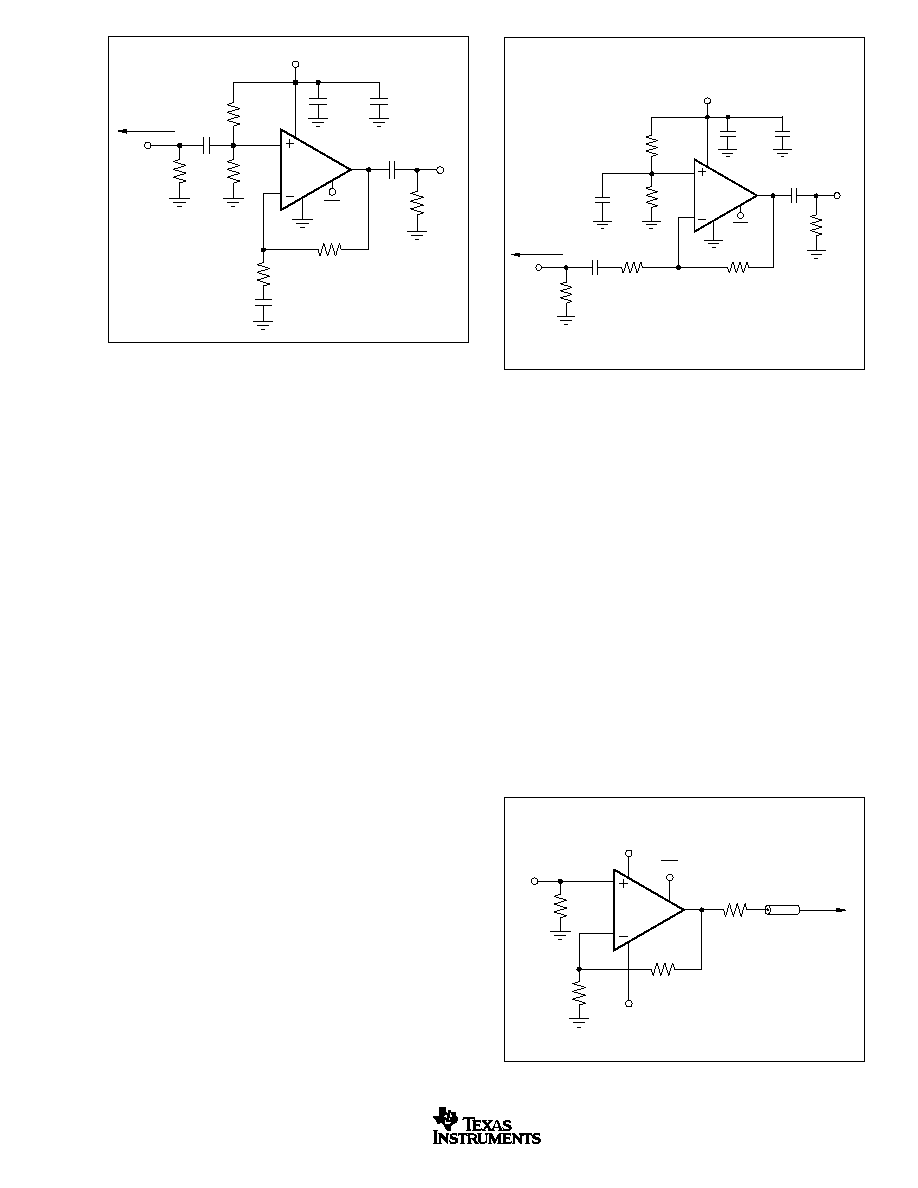
VERY LOW POWER ACTIVE FILTER
The OPA683 provides an exceptionally capable gain block
for implementing Sallen-Key type filters. Typically, the band-
width interaction with gain setting for low power amplifiers,
constrain these filters to using unity-gain amplifiers. Since
the OPA683 CFB
plus
design holds very high bandwidth to
high gains, implementations that provide signal gain, as well
as the desired filter shape, are easily implemented. Figure 6
shows an example of a 5MHz 2nd-order low-pass filter where
the amplifier is providing a voltage gain of 4. This single-
supply implementation (applicable to single +12V operation
as well) consumes only 5.1mW quiescent power. The two
12.5k
resistors bias the input and output at the supply
midpoint while the three 0.1
µ
F capacitors block off the DC
current paths to ground for this mid-scale operating point.
The filter resistors and capacitors have been adjusted
to provide a Butterworth (Q = 0.707) response with a
Wo = 2
∑ 5MHz. This gives a flat passband response with
a ≠3dB cutoff at 5MHz. Figure 7 shows the small-signal
frequency response for the circuit of Figure 6.
HIGH GAIN HF AMPLIFIER
Where high gains at moderate frequencies are required in an
HF receiver channel, the OPA683 can provide a very low
power solution with moderate input noise figure. Figure 8
shows a technique that can improve the noise figure with no
added power. An input transformer provides a noiseless
voltage gain at the cost of higher source impedance for the
amplifier's noninverting input current noise. The circuit of
Figure 8, using a 1:4 turns ratio (1:16 impedance ratio)
transformer, reduces the input noise figure from about 20dB
for just the amplifier to 10.6dB in combination. The bandwidth
for this circuit will be principally set by the transformer since
the OPA683 will give > 80MHz for the gain of 20V/V shown
in Figure 8. The overall circuit gives a gain to a matched 50
load of 32dB (40V/V) from the transformer input. This ex-
ample circuit provides this gain using only 10mW of quies-
cent power with application from 500kHz to 30MHz.
1.4k
OPA683
+5V
12.5k
12.5k
467
0.1
µ
F
V
I
0.1
µ
F
446
157
100pF
Supply
De-coupling
Not Shown
V
O
1k
150pF
0.1
µ
F
15
12
9
6
3
0
≠3
≠6
≠9
Frequency (Hz)
10
3
20E6
10
5
10
4
10
6
10
7
LOW POWER 5MHz LP ACTIVE FILTER
Gain (dB)
FIGURE 6. 5MHz, 2nd-Order Low Pass Filter.
FIGURE 7. Low Power Active Filter Frequency Response.
OPA683
+5V
≠5V
50
50
63
0.01
µ
F
800
P
I
P
O
P
O
= 32dB
P
I
1.2k
50
10.6dB
Noise Figure
1:4
FIGURE 8. Low Power, High Gain HF Amplifier.
LOW POWER, ADC DRIVER
Where a low power, single-supply interface to a single-ended
input +5V ADC is required, the circuit of Figure 9 can provide
a very flexible, high performance solution. Running in an AC-
coupled inverting mode allows the noninverting input to be
used for the common-mode voltage from the ADS820 con-
verter. This midpoint reference biases both the noninverting
converter input and the amplifier noninverting input. With an
AC-coupled gain path, this +2.5V DC bias has a gain of +1
to the output putting the output at the DC midpoint for the
converter. The output then drives through an isolating resis-
tor (60
) to the inverting input of the converter which is
further decoupled by a 22pF external capacitance to add to
its 5pF input capacitance. This coupling network provides a
high cutoff low-pass while also giving a low source imped-
ance at high frequencies for the converter. The gain for this
circuit is set by adjusting R
G
to the desired value. For a 2Vp-p
maximum output driving the light load of Figure 9, the
OPA683 will provide < ≠80dBc THD through 1MHz as shown
in the Typical Characteristics. One of the important advan-
tages for this CFB
plus
amplifier is that this distortion does not
degrade significantly at higher gains.

OPA683
15
SBOS221B
www.ti.com
DESIGN-IN TOOLS
DEMONSTRATION BOARDS
Two PC boards are available to assist in the initial evaluation
of circuit performance using the OPA683 in its two package
styles. Both of these are available free as an unpopulated PC
board delivered with descriptive documentation. The sum-
mary information for these boards is shown in Table I.
The buffer gain is typically very close to 1.00 and is normally
neglected from signal gain considerations. It will, however
set the CMRR for a single op amp differential amplifier
configuration. For the buffer gain
< 1.0, the CMRR =
≠20 ∑ log(1 ≠
). The closed loop input stage buffer used in
the OPA683 gives a buffer gain more closely approaching
1.00 and this shows up in a slightly higher CMRR than any
previous current feedback op amp. The 60dB typical CMRR
shown in the Electrical Characteristics implies a buffer gain
of 0.9990.
R
I
, the buffer output impedance, is a critical portion of the
bandwidth control equation. The OPA683 reduces this ele-
ment to approximately 4.5
using the loop-gain of the input
buffer stage. This significant reduction in buffer output im-
pedance, on very low power, contributes significantly to
extending the bandwidth at higher gains.
BOARD
LITERATURE
PART
REQUEST
PRODUCT
PACKAGE
NUMBER
NUMBER
OPA683ID
SO-8
DEM-OPA68xU
SBOU009
OPA683IDBQ
SOT23-6
DEM-OPA6xxN
SBOU010
TABLE I. EVM Boards by Package.
OPERATING SUGGESTIONS
SETTING RESISTOR VALUES TO OPTIMIZE
BANDWIDTH
Any current-feedback op amp like the OPA683 can hold high
bandwidth over signal gain settings with the proper adjust-
ment of the external resistor values. A low-power part like the
OPA683 typically shows a larger change in bandwidth due to
the significant contribution of the inverting input impedance
to loop-gain changes as the signal gain is changed. Figure
10 shows a simplified analysis circuit for any current feed-
back amplifier.
The key elements of this current feedback op amp model are:
Buffer gain from the noninverting input to the inverting input
R
I
Buffer output impedance
i
ERR
Feedback error current signal
Z(s)
Frequency dependent open loop transimpedance gain
from i
ERR
to V
O
OPA683
+5V
DIS
60
R
G
R
G
R
I
1.4k
50
22pF
V
I
V
O
1.4k
0.1
µ
F
V
O
= ≠
V
I
IN
IN
CM
ADS830
10-Bit
20MSPS
2.5V
DC
+2.5V
2Vp-p
Max
FIGURE 9. Low Power, Single-Supply, ADC Driver.
R
F
V
O
R
G
R
I
Z
(S)
i
ERR
i
ERR
V
I
FIGURE 10. Current Feedback Transfer Function Analysis
Circuit.

OPA683
16
SBOS221B
www.ti.com
A current-feedback op amp senses an error current in the
inverting node (as opposed to a differential input error volt-
age for a voltage feedback op amp) and passes this on to the
output through an internal frequency dependent transimped-
ance gain. The Typical Characteristics show this open-loop
transimpedance response. This is analogous to the open-
loop voltage gain curve for a voltage feedback op amp.
Developing the transfer function for the circuit of Figure 10
gives Equation 1:
(1)
V
V
R
R
R
R
R
R
Z
NG
R
R NG
Z
NG
R
R
O
I
F
G
F
I
F
G
S
F
I
S
F
G
=
+
+
+
+
=
+
+
=
+
1
1
1
1
1
( )
( )
This is written in a loop-gain analysis format where the errors
arising from a non-infinite open-loop gain are shown in the
denominator. If Z(s) was infinite over all frequencies, the
denominator of Equation 1 would reduce to 1 and the ideal
desired signal gain shown in the numerator would be achieved.
The fraction in the denominator of Equation 1 determines the
frequency response. Equation 2 shows this as the loop-gain
equation.
(2)
Z
R
R NG
Loop Gain
S
F
I
( )
+
=
If 20 ∑ log(R
F
+ NG ∑ R
I
) were drawn on top of the open-loop
transimpedance plot, the difference between the two would
be the loop gain at a given frequency. Eventually, Z(s) rolls
off to equal the denominator of Equation 2 at which point the
loop gain has reduced to 1 (and the curves have intersected).
This point of equality is where the amplifier's closed-loop
frequency response given by Equation 1 will start to roll off,
and is exactly analogous to the frequency at which the noise
gain equals the open-loop voltage gain for a voltage feed-
back op amp. The difference here is that the total impedance
in the denominator of Equation 2 may be controlled some-
what separately from the desired signal gain (or NG).
The OPA683 is internally compensated to give a maximally
flat frequency response for R
F
= 1.2k
at NG = 2 on
±
5V
supplies. That optimum value goes to 1.4k
on a single +5V
supply. Normally, with a current feedback amplifier, it is
possible to adjust the feedback resistor to hold this band-
width up as the gain is increased. The CFB
plus
architecture
has reduced the contribution of the inverting input impedance
to provide exceptional bandwidth to higher gains without
adjusting the feedback resistor value. The Typical Character-
istics show the small-signal bandwidth over gain with a fixed
feedback resistor.
At very high gains, 2nd-order effects in the buffer output
impedance cause the overall response to peak up. If desired,
it is possible to retain a flatter frequency response at higher
gains by adjusting the feedback resistor to higher values as
the gain is increased. Figure 11 shows the empirically deter-
mined feedback resistor and resulting ≠3dB bandwidth from
gains of +2 to +100 to hold a < 0.5dB peaked response.
Here, since a slight peaking was allowed, a lower nominal R
F
is suggested at a gain of +2 giving > 250MHz bandwidth.
This exceeds that shown in the Electrical Characteristics due
to the slightly lower feedback resistor allowing a modest
peaking in the response. Figure 12 shows the measured
frequency response curves with the adjusted feedback resis-
tor value. While the bandwidth for this low-power part does
reduce at higher gains, going over a 50:1 gain range gives
only a factor of 10 bandwidth reduction. The 25MHz band-
width at a gain of 100V/V is equivalent to a 2.5GHz gain
bandwidth product voltage feedback amplifier capability. Even
better bandwidth retention to higher gains can be delivered
by the slightly higher quiescent power OPA684.
3900
3400
2900
2400
1900
1400
900
Voltage Gain (V/V)
2
20
10
R
F
5
50
100
Feedback Resistor (
)
325
275
225
175
125
75
25
Bandwidth (MHz)
≠3dB Bandwidth
V
O
= 0.5Vp-p
3
0
≠3
≠6
≠9
≠12
Frequency (MHz)
1
200
10
100
Normalized Gain (dB)
G = 5
G = 100
G = 2
G = 10
G = 50
G = 20
FIGURE 11. Bandwidth and R
F
Optimized vs Gain.
FIGURE 12. Small-Signal Frequency Response with Opti-
mized R
F
.

OPA683
17
SBOS221B
www.ti.com
OUTPUT CURRENT AND VOLTAGE
The OPA683 provides output voltage and current capabilities
that can support the needs of driving doubly-terminated 50
lines. Changing the 1k
load in Figure 1 to a 100
will give
a total load that is the parallel combination of the 100
load
and the 2.4k
total feedback network impedance. This 96
load will require no more than 36mA output current to support
a
±
3.5V output voltage swing. This is within the specified
minimum output current of +58mA/≠45mA over the full tem-
perature range.
The specifications described above, though familiar in the
industry, consider voltage and current limits separately. In
many applications, it is the voltage ∑ current, or V-I product,
which is more relevant to circuit operation. Refer to the
"Output Voltage and Current Limitations" plot in the Typical
Characteristics. The X and Y axes of this graph show the
zero-voltage output current limit and the zero-current output
voltage limit, respectively. The four quadrants give a more
detailed view of the OPA683's output drive capabilities.
Superimposing resistor load lines onto the plot shows the
available output voltage and current for specific loads.
The minimum specified output voltage and current over
temperature are set by worst-case simulations at the cold
temperature extreme. Only at cold startup will the output
current and voltage decrease to the numbers shown in the
Electrical Specifications. As the output transistors deliver
power, their junction temperatures will increase, decreasing
their V
BE
's (increasing the available output voltage swing)
and increasing their current gains (increasing the available
output current). In steady state operation, the available
output voltage and current will always be greater than that
shown in the over-temperature specifications since the out-
put stage junction temperatures will be higher than the
minimum specified operating ambient.
To maintain maximum output stage linearity, no output short
circuit protection is provided. This will not normally be a
problem since most applications include a series matching
resistor at the output that will limit the internal power dissipa-
tion if the output side of this resistor is shorted to ground.
However, shorting the output pin directly to the adjacent
positive power-supply pin (8-pin packages) will, in most
cases, destroy the amplifier. If additional short-circuit protec-
tion is required, consider a small series resistor in the power-
supply leads. This will, under heavy output loads, reduce the
available output voltage swing. A 5
series resistor in each
power-supply lead will limit the internal power dissipation to
less than 1W for an output short circuit while decreasing the
available output voltage swing only 0.25V for up to 50mA
desired load currents. Always place the 0.1
µ
F power-supply
decoupling capacitors after these supply current limiting
resistors directly on the supply pins.
DRIVING CAPACITIVE LOADS
One of the most demanding and yet very common load
conditions for an op amp is capacitive loading. Often, the
capacitive load is the input of an ADC--including additional
external capacitance which may be recommended to im-
prove ADC linearity. A high-speed, high open-loop gain
amplifier like the OPA683 can be very susceptible to de-
creased stability and closed-loop response peaking when a
capacitive load is placed directly on the output pin. When the
amplifier's open-loop output resistance is considered, this
capacitive load introduces an additional pole in the signal
path that can decrease the phase margin. Several external
solutions to this problem have been suggested. When the
primary considerations are frequency response flatness, pulse
response fidelity and/or distortion, the simplest and most
effective solution is to isolate the capacitive load from the
feedback loop by inserting a series isolation resistor between
the amplifier output and the capacitive load. This does not
eliminate the pole from the loop response, but rather shifts it
and adds a zero at a higher frequency. The additional zero
acts to cancel the phase lag from the capacitive load pole,
thus increasing the phase margin and improving stability.
The Typical Characteristics show the recommended "R
S
vs
Capacitive Load" and the resulting frequency response at the
load. The 1k
resistor shown in parallel with the load
capacitor is a measurement path and may be omitted.
Parasitic capacitive loads greater than 3pF can begin to
degrade the performance of the OPA683. Long PC board
traces, unmatched cables, and connections to multiple de-
vices can easily cause this value to be exceeded. Always
consider this effect carefully, and add the recommended
series resistor as close as possible to the OPA683 output pin
(see Board Layout Guidelines).
DISTORTION PERFORMANCE
The OPA683 provides low distortion in a very low power
amplifier. The CFB
plus
architecture also gives two significant
areas of distortion improvement. First, in operating regions
where the 2nd-harmonic distortion due to output stage
nonlinearities is very low (frequencies < 1MHz, low output
swings into light loads) the linearization at the inverting node
provided by the CFB
plus
design gives 2nd-harmonic distor-
tions that extend into the ≠90dBc region. Previous current
feedback amplifiers have been limited to approximately
≠85dBc due to the nonlinearities at the inverting input. The
second area of distortion improvement comes in a distortion
performance that is more gain independent than prior solu-
tions. To the extent that the distortion at a particular output
power is output stage dependent, 2nd-harmonic particularly,
and to a lesser extend 3rd-harmonic distortion, is constant as
the gain is increased. This is due to the constant loop gain
versus signal gain provided by the CFB
plus
design. As shown
in the Typical Characteristics, while the 2nd-harmonic is
constant with gain, the 3rd-harmonic degrades at higher
gains.
Relative to alternative amplifiers with < 1mA supply current,
the OPA683 holds much lower distortion at higher frequen-
cies (> 5MHz) and to higher gains. Generally, until the
fundamental signal reaches very high frequency or power
levels, the 2nd-harmonic will dominate the distortion with a
lower 3rd-harmonic component. Focusing then on the 2nd-
harmonic, increasing the load impedance improves distortion
slightly for the OPA683. Remember that the total load in-

OPA683
18
SBOS221B
www.ti.com
cludes the feedback network--in the noninverting configura-
tion (see Figure 1) this is the sum of R
F
+ R
G
, while in the
inverting configuration it is just R
F
. Also, providing an addi-
tional supply decoupling capacitor (0.1
µ
F) between the sup-
ply pins (for bipolar operation) improves the 2nd-order distor-
tion slightly (3dB to 6dB).
In most op amps, increasing the output voltage swing in-
creases harmonic distortion directly. A low-power part like the
OPA683 includes quiescent boost circuits to provide the full-
power bandwidth shown. These act to increase the bias in a
very linear fashion only when high slew rate or output power
are required. The Typical Characteristics show the 2nd-har-
monic increasing slightly from 500mVp-p to 5Vp-p outputs
while the 3rd-harmonics also increase with output power.
The OPA683 has an extremely low 3rd-order harmonic distor-
tion--particularly for light loads and at lower frequencies. This
also gives low 2-tone, 3rd-order intermodulation distortion as
shown in the Typical Characteristics. Since the OPA683
includes internal power boost circuits to retain good full-power
performance at high frequencies and outputs, it does not show
a classical 2-tone, 3rd-order intermodulation intercept charac-
teristic. Instead, it holds relatively low and constant 3rd-order
intermodulation spurious levels over power. The Typical Char-
acteristics show this spurious level as a dBc below the carrier
at fixed center frequencies swept over single-tone voltage
swing at a 1k
load. Very light loads such as ADC inputs for
will see < ≠85dBc 3rd-order spurious to 1MHz for full-scale
inputs. For much lower 3rd-order intermodulation distortion
through 200MHz, consider the OPA685.
NOISE PERFORMANCE
Wideband current-feedback op amps generally have a higher
output noise than comparable voltage feedback op amps. The
OPA683 offers an excellent balance between voltage and
current noise terms to achieve low output noise in a low- power
amplifier. The inverting current noise (11.6pA/
Hz) is lower
than most other current feedback op amps while the input
voltage noise (4.4nV/
Hz) is lower than any unity-gain stable,
comparable slew rate, voltage feedback op amp. This low input
voltage noise was achieved at the price of higher noninverting
input current noise (5.1pA/
Hz). As long as the AC source
impedance looking out of the noninverting node is less than
300
, this current noise will not contribute significantly to the
total output noise. The op amp input voltage noise and the two
input current noise terms combine to give low output noise
under a wide variety of operating conditions. Figure 13 shows
the op amp noise analysis model with all the noise terms
included. In this model, all noise terms are taken to be noise
voltage or current density terms in either nV/
Hz or pA/
Hz.
The total output spot noise voltage can be computed as the
square root of the sum of all squared output noise voltage
contributors. Equation 3 shows the general form for the
output noise voltage using the terms shown in Figure 13.
(3)
E
E
I
R
kTR
G
I R
kTR G
O
NI
BN S
S
N
BI F
F
N
=
+
(
)
+
+
(
)
+
2
2
2
2
4
4
4kT
R
G
R
G
R
F
R
S
OPA683
I
BI
E
O
I
BN
4kT = 1.6E ≠20J
at 290
∞
K
E
RS
E
NI
4kTR
S
4kTR
F
Dividing this expression by the noise gain (NG = (1 + R
F
/R
G
))
will give the equivalent input referred spot noise voltage at the
noninverting input, as shown in Equation 4.
(4)
E
E
I
R
kTR
I R
G
kTR
G
N
NI
BN S
S
BI F
N
F
N
=
+
(
)
+
+
+
2
2
2
4
4
Evaluating these two equations for the OPA683 circuit and
component values (see Figure 1) will give a total output spot
noise voltage of 17.6nV/
Hz and a total equivalent input spot
noise voltage of 8.8nV/
Hz. This total input referred spot
noise voltage is higher than the 4.4nV/
Hz specification for
the op amp voltage noise alone. This reflects the noise
added to the output by the inverting current noise times the
feedback resistor. As the gain is increased, this fixed output
noise power term contributes less to the total output noise
and the total input referred voltage noise given by Equation
3 will approach just the 4.4nV/
Hz of the op amp itself. For
example, going to a gain of +20 in the circuit of Figure 1,
adjusting only the gain resistor to 63.2
, will give a total input
referred noise of 4.6nV/
Hz. A more complete description of
op amp noise analysis can be found in the TI application note
AB-103 (SBOA066). Refer to Texas Instruments' web site
www.ti.com.
DC ACCURACY AND OFFSET CONTROL
A current-feedback op amp like the OPA683 provides excep-
tional bandwidth in high gains, giving fast pulse settling but
only moderate DC accuracy. The Electrical Characteristics
show an input offset voltage comparable to high slew rate
voltage-feedback amplifiers. However, the two input bias
currents are somewhat higher and are unmatched. Whereas
bias current cancellation techniques are very effective with
most voltage feedback op amps, they do not generally
reduce the output DC offset for wideband current-feedback
op amps. Since the two input bias currents are unrelated in
both magnitude and polarity, matching the source imped-
ance looking out of each input to reduce their error contribu-
tion to the output is ineffective. Evaluating the configuration
of Figure 1, using worst case +25
∞
C input offset voltage and
FIGURE 13. Op Amp Noise Analysis Model.

OPA683
19
SBOS221B
www.ti.com
the two input bias currents, gives a worst case output offset
range equal to:
±
(NG ∑ V
OS(MAX)
)
±
(I
BN
∑ R
S
/2 ∑ NG)
±
(I
BI
∑ R
F
)
where
NG = noninverting signal gain
=
±
(2 ∑ 3.5mV)
±
(4
µ
A ∑ 25
∑ 2)
±
(1.2k
∑ 10
µ
A)
=
±
7mV
±
0.1mV
±
12mV
=
±
19.1mV
While the last term, the inverting bias current error, is dominant
in this low-gain circuit, the input offset voltage will become the
dominant DC error term as the gain exceeds 4V/V. Where
improved DC precision is required in a high-speed amplifier,
consider the OPA642 single and OPA2822 dual voltage-
feedback amplifiers.
DISABLE OPERATION
The OPA683 provides an optional disable feature that may
be used to reduce system power when channel operation is
not required. If the V
DIS
control pin is left unconnected, the
OPA683 will operate normally. To disable, the control pin
must be asserted LOW. Figure 14 shows a simplified internal
circuit for the disable control feature.
In normal operation, base current to Q1 is provided through
the 250k
resistor while the emitter current through the 40k
resistor sets up a voltage drop that is inadequate to turn on
the two diodes in Q1's emitter. As V
DIS
is pulled LOW,
additional current is pulled through the 40k
resistor eventu-
ally turning on these two diodes (
33
µ
A). At this point, any
further current pulled out of V
DIS
goes through those diodes
holding the emitter-base voltage of Q1 at approximately 0V.
25k
250k
40k
I
S
Control
≠V
S
+V
S
V
DIS
Q1
FIGURE 14. Simplified Disable Control Circuit.
This shuts off the collector current out of Q1, turning the
amplifier off. The supply current in the disable mode are only
those required to operate the circuit of Figure 14.
When disabled, the output and input nodes go to a high
impedance state. If the OPA683 is operating in a gain of +1
(with a 1.2k
feedback resistor still required for stability), this
will show a very high impedance (1.7pF || 1M
) at the output
and exceptional signal isolation. If operating at a gain greater
than +1, the total feedback network resistance (R
F
+ R
G
) will
appear as the impedance looking back into the output, but
the circuit will still show very high forward and reverse
isolation. If configured as an inverting amplifier, the input and
output will be connected through the feedback network
resistance (R
F
+ R
G
) giving relatively poor input to output
isolation.
The OPA683 provides very high power gain on low quiescent
current levels. When disabled, internal high impedance nodes
discharge slowly which, with the exceptional power gain
provided, give a self powering characteristic that leads to a
slow turn off characteristic. Typical full turn off times to rated
100
µ
A disabled supply current are 60ms. Turn on times are
very fast--less than 40ns.
THERMAL ANALYSIS
The OPA683 will not require external heat-sinking for most
applications. Maximum desired junction temperature will set
the maximum allowed internal power dissipation as de-
scribed below. In no case should the maximum junction
temperature be allowed to exceed 175
∞
C.
Operating junction temperature (T
J
) is given by T
A
+ P
D
∑
JA
.
The total internal power dissipation (P
D
) is the sum of
quiescent power (P
DQ
) and additional power dissipated in the
output stage (P
DL
) to deliver load power. Quiescent power is
simply the specified no-load supply current times the total
supply voltage across the part. P
DL
will depend on the
required output signal and load but would, for a grounded
resistive load, be at a maximum when the output is fixed at
a voltage equal to 1/2 either supply voltage (for equal bipolar
supplies). Under this condition P
DL
= V
S
2
/(4 ∑ R
L
) where R
L
includes feedback network loading.
Note that it is the power in the output stage and not into the
load that determines internal power dissipation.
As an absolute worst case example, compute the maximum
T
J
using an OPA683IDBV (SOT23-6 package) in the circuit
of Figure 1 operating at the maximum specified ambient
temperature of +85
∞
C and driving a grounded 100
load.
P
D
= 10V ∑ 1.05mA + 5
2
/(4 ∑ (100
|| 2.4k
)) = 76mW
Maximum T
J
= +85
∞
C + (0.076W ∑ 150
∞
C/W) = 96
∞
C.
This maximum operating junction temperature is well below
most system level targets. Most applications will be lower
than this since an absolute worst case output stage power
was assumed in this calculation.

OPA683
20
SBOS221B
www.ti.com
BOARD LAYOUT GUIDELINES
Achieving optimum performance with a high frequency am-
plifier like the OPA683 requires careful attention to board
layout parasitics and external component types. Recommen-
dations that will optimize performance include:
a) Minimize parasitic capacitance to any AC ground for
all of the signal I/O pins. Parasitic capacitance on the
output and inverting input pins can cause instability: on
the noninverting input, it can react with the source imped-
ance to cause unintentional band-limiting.. To reduce
unwanted capacitance, a window around the signal I/O
pins should be opened in all of the ground and power
planes around those pins. Otherwise, ground and power
planes should be unbroken elsewhere on the board.
b) Minimize the distance (< 0.25") from the power-supply
pins to high frequency 0.1
µ
F decoupling capacitors.
At the device pins, the ground and power-plane layout
should not be in close proximity to the signal I/O pins.
Avoid narrow power and ground traces to minimize induc-
tance between the pins and the decoupling capacitors.
The power-supply connections should always be decoupled
with these capacitors. An optional supply decoupling
capacitor across the two power supplies (for bipolar op-
eration) will improve 2nd-harmonic distortion performance.
Larger (2.2
µ
F to 6.8
µ
F) decoupling capacitors, effective at
lower frequency, should also be used on the main supply
pins. These may be placed somewhat farther from the
device and may be shared among several devices in the
same area of the PC board.
c) Careful selection and placement of external compo-
nents will preserve the high frequency performance
of the OPA683. Resistors should be a very low reactance
type. Surface-mount resistors work best and allow a
tighter overall layout. Metal film and carbon composition
axially-leaded resistors can also provide good high fre-
quency performance. Again, keep their leads and PC
board trace length as short as possible. Never use wire-
wound type resistors in a high-frequency application.
Since the output pin and inverting input pin are the most
sensitive to parasitic capacitance, always position the
feedback and series output resistor, if any, as close as
possible to the output pin. Other network components,
such as noninverting input termination resistors, should
also be placed close to the package. Where double side
component mounting is allowed, place the feedback resis-
tor directly under the package on the other side of the
board between the output and inverting input pins. The
frequency response is primarily determined by the feed-
back resistor value as described previously. Increasing its
value will reduce the peaking at higher gains, while
decreasing it will give a more peaked frequency response
at lower gains. The 1.2k
feedback resistor used in the
Electrical Characteristics at a gain of +2 on
±
5V supplies
is a good starting point for design. Note that a 1.2k
feedback resistor, rather than a direct short, is required for
the unity-gain follower application. A current-feedback op
amp requires a feedback resistor even in the unity-gain
follower configuration to control stability.
d) Connections to other wideband devices on the board
may be made with short direct traces or through
onboard transmission lines. For short connections, con-
sider the trace and the input to the next device as a
lumped capacitive load. Relatively wide traces (50mils to
100mils) should be used, preferably with ground and
power planes opened up around them. Estimate the total
capacitive load and set R
S
from the plot of recommended
R
S
versus capacitive load. Low parasitic capacitive loads
(< 5pF) may not need an R
S
since the OPA683 is
nominally compensated to operate with a 2pF parasitic
load. If a long trace is required, and the 6dB signal loss
intrinsic to a doubly-terminated transmission line is ac-
ceptable, implement a matched impedance transmission
line using microstrip or stripline techniques (consult an
ECL design handbook for microstrip and stripline layout
techniques). A 50
environment is normally not neces-
sary on board, and in fact a higher impedance environ-
ment will improve distortion as shown in the distortion
versus load plots. With a characteristic board trace imped-
ance defined based on board material and trace dimen-
sions, a matching series resistor into the trace from the
output of the OPA683 is used as well as a terminating
shunt resistor at the input of the destination device.
Remember also that the terminating impedance will be
the parallel combination of the shunt resistor and the input
impedance of the destination device: this total effective
impedance should be set to match the trace impedance.
The high output voltage and current capability of the
OPA683 allows multiple destination devices to be handled
as separate transmission lines, each with their own series
and shunt terminations. If the 6dB attenuation of a doubly-
terminated transmission line is unacceptable, a long trace
can be series-terminated at the source end only. Treat the
trace as a capacitive load in this case and set the series
resistor value as shown in the plot of "R
S
vs Capacitive
Load". This will not preserve signal integrity as well as a
doubly-terminated line. If the input impedance of the
destination device is LOW, there will be some signal
attenuation due to the voltage divider formed by the series
output into the terminating impedance.
e) Socketing a high-speed part like the OPA683 is not
recommended. The additional lead length and pin-to-pin
capacitance introduced by the socket can create an ex-
tremely troublesome parasitic network which can make it
almost impossible to achieve a smooth, stable frequency
response. Best results are obtained by soldering the
OPA683 onto the board.

OPA683
21
SBOS221B
www.ti.com
INPUT AND ESD PROTECTION
The OPA683 is built using a very high speed complementary
bipolar process. The internal junction breakdown voltages
are relatively low for these very small geometry devices.
These breakdowns are reflected in the Absolute Maximum
Ratings table where an absolute maximum 13V across the
supply pins is reported. All device pins have limited ESD
protection using internal diodes to the power supplies as
shown in Figure 15.
These diodes provide moderate protection to input overdrive
voltages above the supplies as well. The protection diodes
can typically support 30mA continuous current. Where higher
currents are possible (e.g. in systems with
±
15V supply parts
driving into the OPA683), current limiting series resistors
should be added into the two inputs. Keep these resistor
values as low as possible since high values degrade both
noise performance and frequency response.
External
Pin
+V
CC
≠V
CC
Internal
Circuitry
FIGURE 15. Internal ESD Protection.

OPA683
22
SBOS221B
www.ti.com
MSOI002B ≠ JANUARY 1995 ≠ REVISED SEPTEMBER 2001
D (R-PDSO-G**)
PLASTIC SMALL-OUTLINE PACKAGE
8 PINS SHOWN
8
0.197
(5,00)
A MAX
A MIN
(4,80)
0.189
0.337
(8,55)
(8,75)
0.344
14
0.386
(9,80)
(10,00)
0.394
16
DIM
PINS **
4040047/E 09/01
0.069 (1,75) MAX
Seating Plane
0.004 (0,10)
0.010 (0,25)
0.010 (0,25)
0.016 (0,40)
0.044 (1,12)
0.244 (6,20)
0.228 (5,80)
0.020 (0,51)
0.014 (0,35)
1
4
8
5
0.150 (3,81)
0.157 (4,00)
0.008 (0,20) NOM
0
∞
≠ 8
∞
Gage Plane
A
0.004 (0,10)
0.010 (0,25)
0.050 (1,27)
NOTES: A. All linear dimensions are in inches (millimeters).
B. This drawing is subject to change without notice.
C. Body dimensions do not include mold flash or protrusion, not to exceed 0.006 (0,15).
D. Falls within JEDEC MS-012
PACKAGE DRAWINGS

OPA683
23
SBOS221B
www.ti.com
PACKAGE DRAWINGS (Cont.)
MPDS018E ≠ FEBRUARY 1996 ≠ REVISED FEBRUARY 2002
DBV (R-PDSO-G5)
PLASTIC SMALL-OUTLINE
0,10
M
0,20
0,95
0
∞
≠ 8
∞
0,25
0,35
0,55
Gage Plane
0,15 NOM
4073253-4/G 01/02
2,60
3,00
0,50
0,30
1,50
1,70
4
5
3
1
2,80
3,00
0,95
1,45
0,05 MIN
Seating Plane
NOTES: A. All linear dimensions are in millimeters.
B. This drawing is subject to change without notice.
C. Body dimensions do not include mold flash or protrusion.
D. Falls within JEDEC MO-178

PACKAGING INFORMATION
ORDERABLE DEVICE
STATUS(1)
PACKAGE TYPE
PACKAGE DRAWING
PINS
PACKAGE QTY
OPA683ID
ACTIVE
SOIC
D
8
100
OPA683IDBVR
ACTIVE
SOP
DBV
6
3000
OPA683IDBVT
ACTIVE
SOP
DBV
6
250
OPA683IDR
ACTIVE
SOIC
D
8
2500
(1) The marketing status values are defined as follows:
ACTIVE: Product device recommended for new designs.
LIFEBUY: TI has announced that the device will be discontinued, and a lifetime-buy period is in effect.
NRND: Not recommended for new designs. Device is in production to support existing customers, but TI does not recommend using this part in
a new design.
PREVIEW: Device has been announced but is not in production. Samples may or may not be available.
OBSOLETE: TI has discontinued the production of the device.
PACKAGE OPTION ADDENDUM
www.ti.com
3-Oct-2003

IMPORTANT NOTICE
Texas Instruments Incorporated and its subsidiaries (TI) reserve the right to make corrections, modifications,
enhancements, improvements, and other changes to its products and services at any time and to discontinue
any product or service without notice. Customers should obtain the latest relevant information before placing
orders and should verify that such information is current and complete. All products are sold subject to TI's terms
and conditions of sale supplied at the time of order acknowledgment.
TI warrants performance of its hardware products to the specifications applicable at the time of sale in
accordance with TI's standard warranty. Testing and other quality control techniques are used to the extent TI
deems necessary to support this warranty. Except where mandated by government requirements, testing of all
parameters of each product is not necessarily performed.
TI assumes no liability for applications assistance or customer product design. Customers are responsible for
their products and applications using TI components. To minimize the risks associated with customer products
and applications, customers should provide adequate design and operating safeguards.
TI does not warrant or represent that any license, either express or implied, is granted under any TI patent right,
copyright, mask work right, or other TI intellectual property right relating to any combination, machine, or process
in which TI products or services are used. Information published by TI regarding third-party products or services
does not constitute a license from TI to use such products or services or a warranty or endorsement thereof.
Use of such information may require a license from a third party under the patents or other intellectual property
of the third party, or a license from TI under the patents or other intellectual property of TI.
Reproduction of information in TI data books or data sheets is permissible only if reproduction is without
alteration and is accompanied by all associated warranties, conditions, limitations, and notices. Reproduction
of this information with alteration is an unfair and deceptive business practice. TI is not responsible or liable for
such altered documentation.
Resale of TI products or services with statements different from or beyond the parameters stated by TI for that
product or service voids all express and any implied warranties for the associated TI product or service and
is an unfair and deceptive business practice. TI is not responsible or liable for any such statements.
Following are URLs where you can obtain information on other Texas Instruments products and application
solutions:
Products
Applications
Amplifiers
amplifier.ti.com
Audio
www.ti.com/audio
Data Converters
dataconverter.ti.com
Automotive
www.ti.com/automotive
DSP
dsp.ti.com
Broadband
www.ti.com/broadband
Interface
interface.ti.com
Digital Control
www.ti.com/digitalcontrol
Logic
logic.ti.com
Military
www.ti.com/military
Power Mgmt
power.ti.com
Optical Networking
www.ti.com/opticalnetwork
Microcontrollers
microcontroller.ti.com
Security
www.ti.com/security
Telephony
www.ti.com/telephony
Video & Imaging
www.ti.com/video
Wireless
www.ti.com/wireless
Mailing Address:
Texas Instruments
Post Office Box 655303 Dallas, Texas 75265
Copyright
2003, Texas Instruments Incorporated