Document Outline
- features
- description
- logic diagram (positive logic)
- equivalent input and output schematic diagrams
- absolute maximum ratings
- recommended operating conditions
- electrical characteristics over recommended operating conditions
- switching characteristics over recommended operating conditions
- PARAMETER MEASUREMENT INFORMATION
- TYPICAL CHARACTERISTICS
- APPLICATION INFORMATION
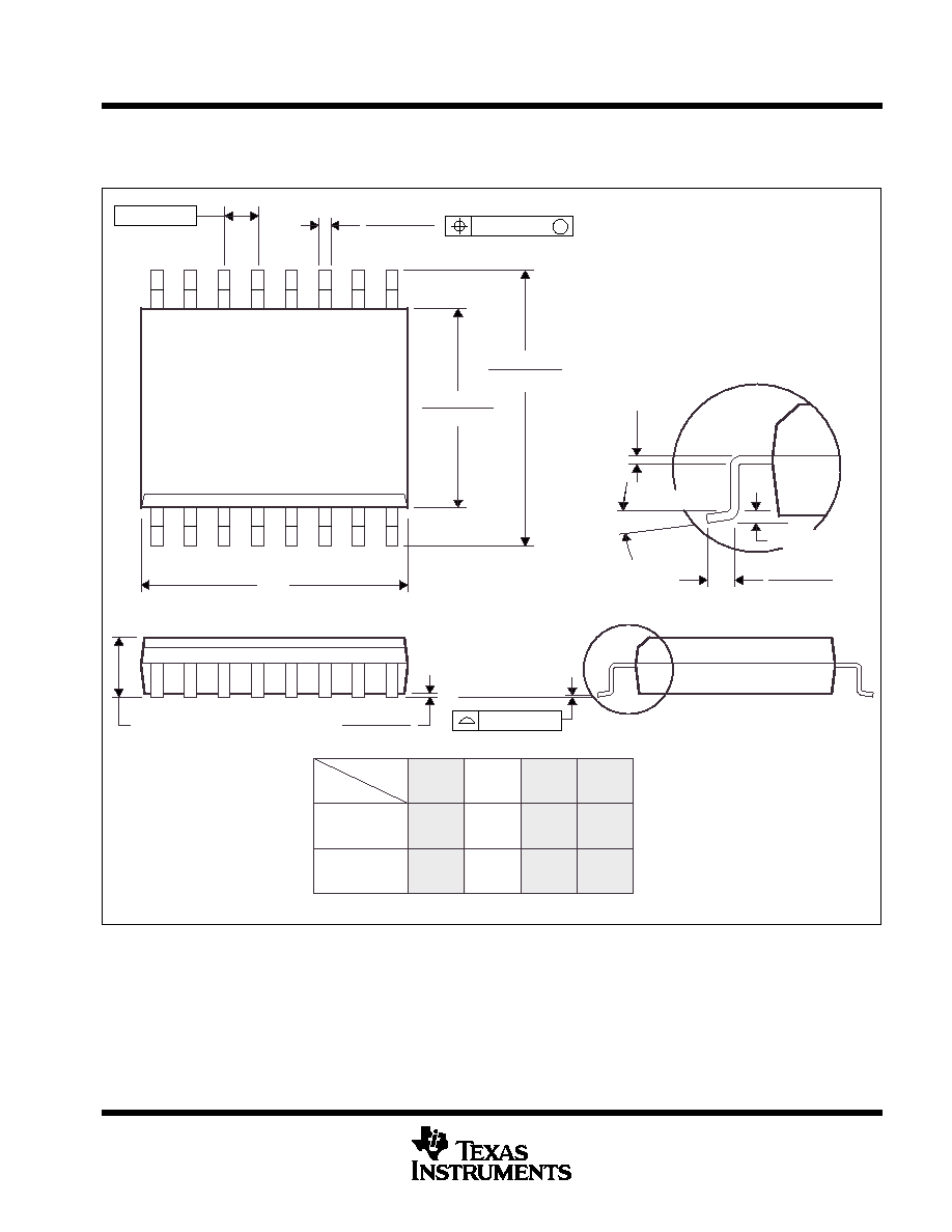
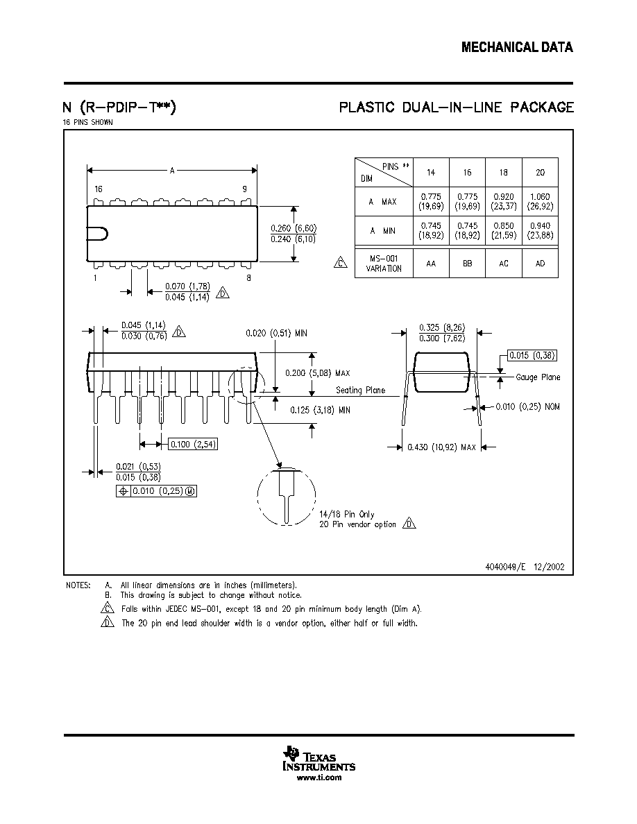
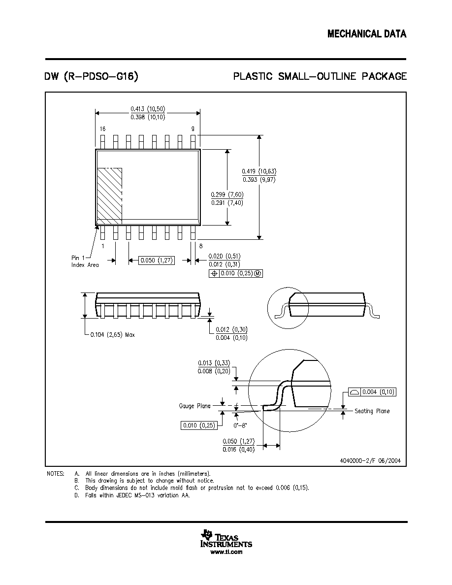
- MECHANICAL DATA
- DW (R-PDSO-G**) PLASTIC SMALL-OUTLINE PACKAGE
- N (R-PDIP-T**) PLASTIC DUAL-IN-LINE PACKAGE
SN65LBC172A, SN75LBC172A
QUADRUPLE RS-485 DIFFERENTIAL LINE DRIVERS
SLLS447B ≠ OCTOBER 2000 ≠ REVISED MAY 2003
1
POST OFFICE BOX 655303
∑
DALLAS, TEXAS 75265
D
Designed for TIA/EIA-485, TIA/EIA-422,
and ISO 8482 Applications
D
Signaling Rates
up to 30 Mbps
D
Propagation Delay Times <11 ns
D
Low Standby Power Consumption
1.5 mA Max
D
Output ESD Protection Exceeds 13 kV
D
Driver Positive- and Negative-Current
Limiting
D
Power-Up and Power-Down Glitch-Free for
Live Insertion Applications
D
Thermal Shutdown Protection
D
Industry Standard Pin-Out, Compatible
With SN75172, AM26LS31, DS96172,
LTC486, and MAX3045
description
The SN65LBC172A and SN75LBC172A are quadruple differential line drivers with 3-state outputs, designed
for TIA/EIA-485 (RS-485), TIA/EIA-422 (RS-422), and ISO 8482 applications.
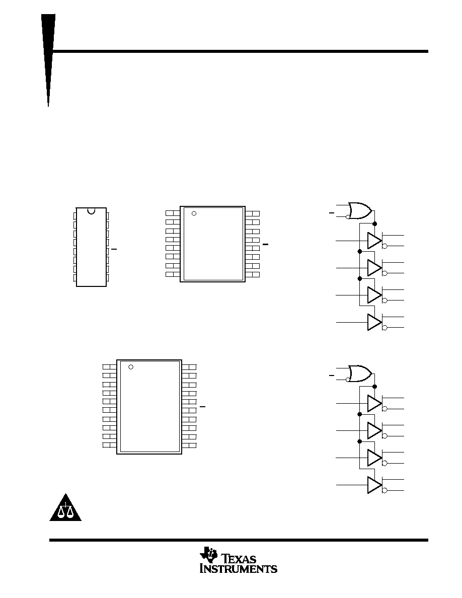
1
2
3
4
5
6
7
8
16
15
14
13
12
11
10
9
1A
1Y
1Z
G
2Z
2Y
2A
GND
V
CC
4A
4Y
4Z
G
3Z
3Y
3A
N PACKAGE
(TOP VIEW)
logic diagram (positive logic)
4Z
4Y
3Z
3Y
2Z
2Y
1Z
1Y
4A
3A
2A
1A
1
7
9
15
G
G
12
4
2
3
6
5
10
11
14
13
4Z
4Y
3Z
3Y
2Z
2Y
1Z
1Y
4A
3A
2A
1A
1
9
11
19
G
G
15
5
2
4
8
6
12
14
18
16
logic diagram (positive logic)
1
2
3
4
5
6
7
8
16
15
14
13
12
11
10
9
1A
1Y
1Z
G
2Z
2Y
2A
GND
V
CC
4A
4Y
4Z
G
3Z
3Y
3A
16-DW PACKAGE
(TOP VIEW)
1
2
3
4
5
6
7
8
9
10
20
19
18
17
16
15
14
13
12
11
1A
1Y
NC
1Z
G
2Z
NC
2Y
2A
GND
V
CC
4A
4Y
NC
4Z
G
3Z
NC
3Y
3A
20-DW PACKAGE
(TOP VIEW)
Copyright
2001 ≠ 2003, Texas Instruments Incorporated
PRODUCTION DATA information is current as of publication date.
Products conform to specifications per the terms of Texas Instruments
standard warranty. Production processing does not necessarily include
testing of all parameters.
Please be aware that an important notice concerning availability, standard warranty, and use in critical applications of
Texas Instruments semiconductor products and disclaimers thereto appears at the end of this data sheet.
LinBiCMOS is a trademark of Texas Instruments.
The signaling rate of a line is the number of voltage transitions that are made per second expressed in the units bps (bits per second).
SN65LBC172A, SN75LBC172A
QUADRUPLE RS-485 DIFFERENTIAL LINE DRIVERS
SLLS447B ≠ OCTOBER 2000 ≠ REVISED MAY 2003
2
POST OFFICE BOX 655303
∑
DALLAS, TEXAS 75265
description (continued)
These devices are optimized for balanced multipoint bus transmission at signalling rates up to 30 million bits
per second. The transmission media may be printed-circuit board traces, backplanes, or cables. The ultimate
rate and distance of data transfer is dependent upon the attenuation characteristics of the media and the noise
coupling to the environment.
Each driver features current limiting and thermal-shutdown circuitry making it suitable for high-speed mulitpoint
data transmission applications in noisy environments. These devices are designed using LinBiCMOS
t
,
facilitating low power consumption and robustness.
The G and G inputs provide driver enable control using either positive or negative logic. When disabled or
powered off, the driver outputs present a high-impedance to the bus for reduced system loading.
The SN75LBC172A is characterized for operation over the temperature range of 0
∞
C to 70
∞
C. The
SN65LBC172A is characterized over the temperature range from ≠40
∞
C to 85
∞
C.
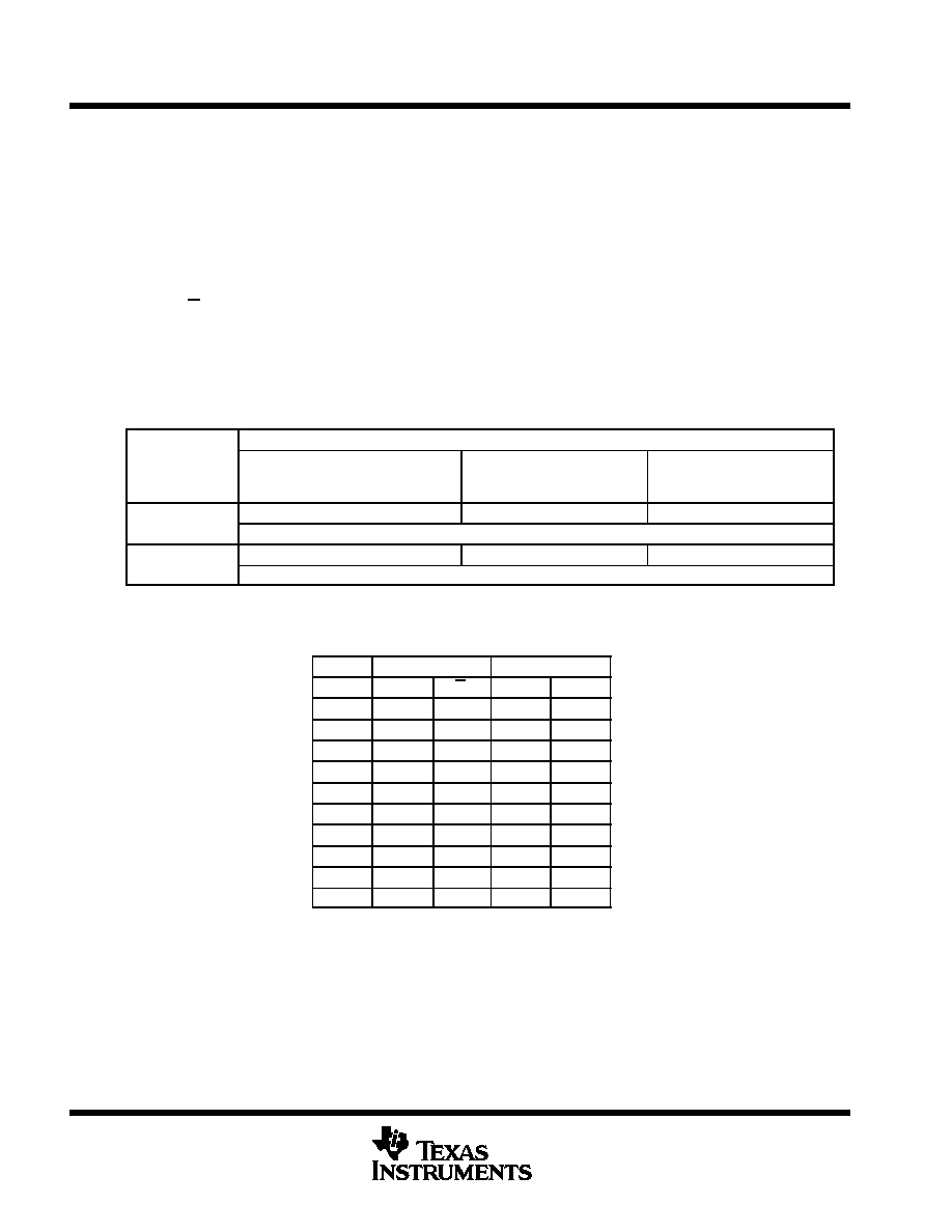
AVAILABLE OPTIONS
PACKAGE
TA
16-PIN PLASTIC
SMALL OUTLINE
(JEDEC MS-013)
20-PIN PLASTIC
SMALL OUTLINE
(JEDEC MS-013)
16-PIN PLASTIC
THROUGH-HOLE
(JEDEC MS-001)
0
∞
C to 70
∞
C
SN75LBC172A16DW
SN75LBC172ADW
SN75LBC172AN
0
∞
C to 70
∞
C
Marked as 75LBC172A
40
∞
C to 85
∞
C
SN65LBC172A16DW
SN65LBC172ADW
SN65LBC172AN
≠ 40
∞
C to 85
∞
C
Marked as 65LBC172A
Add R suffix for taped and reeled version.
FUNCTION TABLE
(EACH DRIVER)
INPUT
ENABLES
OUTPUTS
A
G
G
Y
Z
L
H
X
L
H
L
X
L
L
H
H
H
X
H
L
H
X
L
H
L
OPEN
H
X
H
L
OPEN
X
L
H
L
H
OPEN
X
H
L
L
OPEN
X
L
H
X
L
H
Z
Z
X
L
OPEN
Z
Z
H = high level, L = low level, X = irrelevant,
Z = high impedance (off)
SN65LBC172A, SN75LBC172A
QUADRUPLE RS-485 DIFFERENTIAL LINE DRIVERS
SLLS447B ≠ OCTOBER 2000 ≠ REVISED MAY 2003
3
POST OFFICE BOX 655303
∑
DALLAS, TEXAS 75265
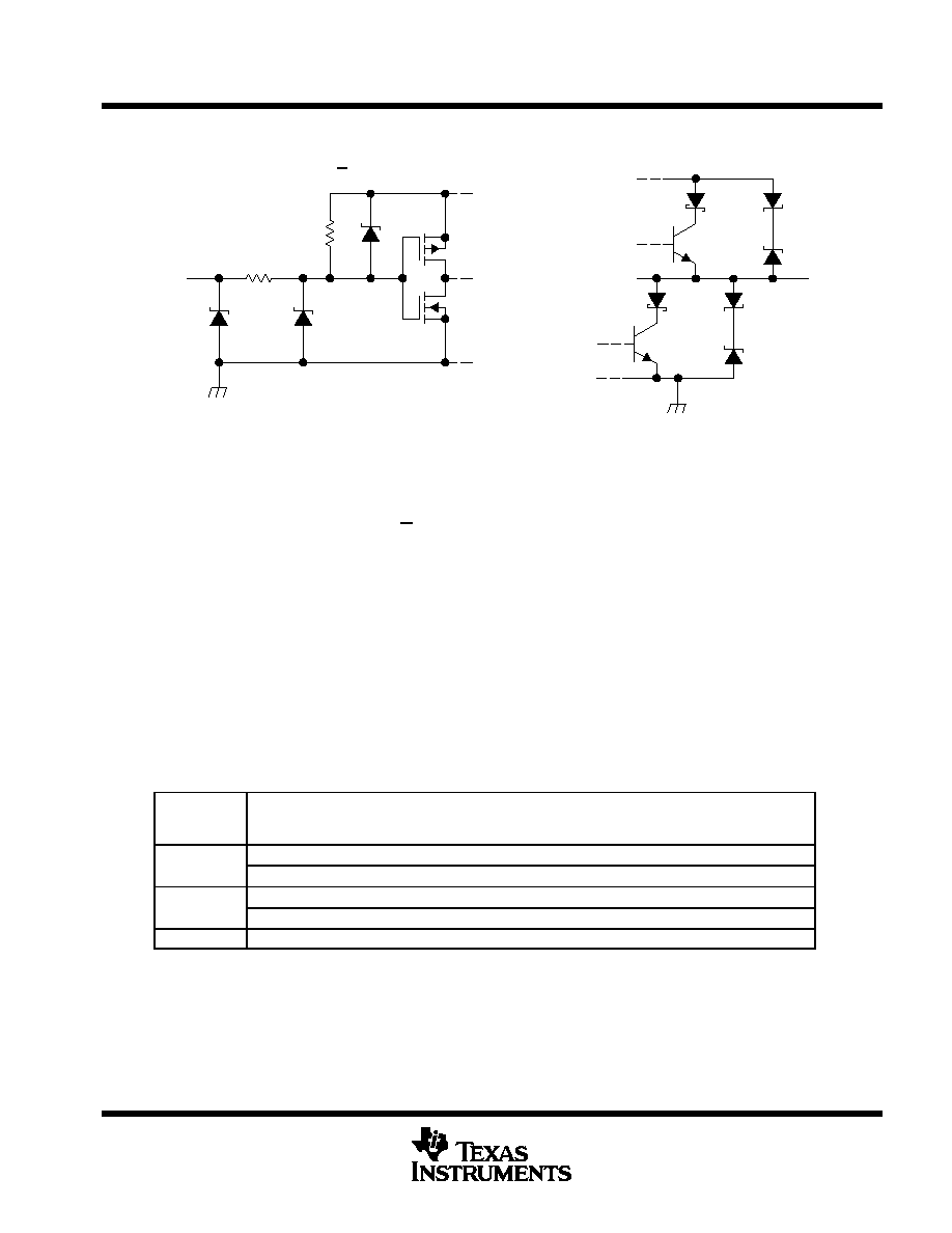
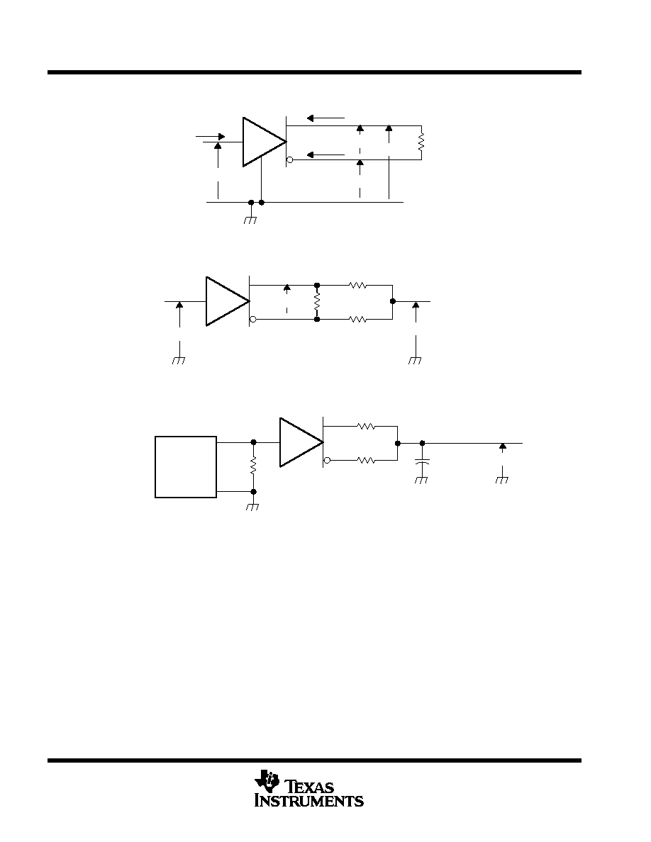
equivalent input and output schematic diagrams
VCC
A, G, or G Input
1 k
9 V
Input
100 k
VCC
Output
16 V
Y or Z Output
16 V
20 V
17 V
16 V
16 V
absolute maximum ratings
Supply voltage range, V
CC
(see Note 1)
≠0.3 V to 6 V
. . . . . . . . . . . . . . . . . . . . . . . . . . . . . . . . . . . . . . . . . . . . . .
Output voltage range, V
O
, at any bus (steady state)
≠10 V to 15 V
. . . . . . . . . . . . . . . . . . . . . . . . . . . . . . . . . . . . . .
Output voltage range, V
O
, at any bus (transient pulse through 100
, see Figure 8)
≠30 V to 30 V
. . . . . . . . . . .
Input voltage range, V
I
, at any A, G, or G terminal
≠0.5 V to V
CC
+ 0.5 V
. . . . . . . . . . . . . . . . . . . . . . . . . . . . . . . .
Electrostatic discharge: Human body model (see Note 2)
Y, Z, and GND
13 kV
. . . . . . . . . . . . . . . . . . . . .
All pins
5 kV
. . . . . . . . . . . . . . . . . . . . . . . . . . . . .
Charged-device model (see Note 3) All pins
1 kV
. . . . . . . . . . . . . . . . . . . . . . . . . . . . .
Storage temperature range, T
stg
≠ 65
∞
C to 150
∞
C
. . . . . . . . . . . . . . . . . . . . . . . . . . . . . . . . . . . . . . . . . . . . . . . . . . .
Continuous power dissipation
See Dissipation Rating Table
. . . . . . . . . . . . . . . . . . . . . . . . . . . . . . . . . . . . . . . . .
Lead temperature 1,6 mm (1/16 inch) from case for 10 seconds
260
∞
C
. . . . . . . . . . . . . . . . . . . . . . . . . . . . . . .
Stresses beyond those listed under "absolute maximum ratings" may cause permanent damage to the device. These are stress ratings only, and
functional operation of the device at these or any other conditions beyond those indicated under "recommended operating conditions" is not
implied. Exposure to absolute-maximum-rated conditions for extended periods may affect device reliability.
NOTES:
1. All voltage values, except differential I/O bus voltages, are with respect to GND.
2. Tested in accordance with JEDEC standard 22, Test Method A114≠A.
3. Tested in accordance with JEDEC standard 22, Test Method C101.
DISSIPATION RATING TABLE
PACKAGE
JEDEC
BOARD
MODEL
TA
25
∞
C
POWER RATING
DERATING FACTOR
ABOVE TA = 25
∞
C
TA = 70
∞
C
POWER RATING
TA = 85
∞
C
POWER RATING
16 PIN DW
Low K
1200 mW
9.6 mW/
∞
C
769 mW
625 mW
16-PIN DW
High K
2240 mW
17.9 mW/
∞
C
1434 mW
1165 mW
20 PIN DW
Low K
1483 mW
11.86 mW/
∞
C
949 mW
771 mW
20-PIN DW
High K
2753 mW
22 mW/
∞
C
1762 mW
1432 mW
16-PIN N
Low K
1150 mW
9.2 mW/
∞
C
736 mW
598 mW
This is the inverse of the junction-to-ambient thermal resistance when board-mounted with no air flow.

SN65LBC172A, SN75LBC172A
QUADRUPLE RS-485 DIFFERENTIAL LINE DRIVERS
SLLS447B ≠ OCTOBER 2000 ≠ REVISED MAY 2003
4
POST OFFICE BOX 655303
∑
DALLAS, TEXAS 75265
recommended operating conditions
MIN
NOM
MAX
UNIT
Supply voltage, VCC
4.75
5
5.25
V
Voltage at any bus terminal
Y, Z
≠7
12
V
High-level input voltage, VIH
A G G
2
VCC
V
Low-level input voltage, VIL
A, G, G
0
0.8
V
Output current
≠60
60
mA
Operating free air temperature T
SN75LBC172A
0
70
∞
C
Operating free-air temperature, TA
SN65LBC172A
≠40
85
∞
C
electrical characteristics over recommended operating conditions
PARAMETER
TEST CONDITIONS
MIN
TYP
MAX
UNIT
VIK
Input clamp voltage
II = ≠18 mA
≠1.5
≠0.77
V
VO
Open-circuit output voltage
Y or Z, No load
0
VCC
V
S
No load (open circuit)
3
VCC
V
Steady-state differential output voltage
R
54
see Figure 1
1
1 6
2 5
V
VOD(SS)
Steady-state differential out ut voltage
magnitude
RL = 54
, see Figure 1
1
1.6
2.5
V
VOD(SS)
magnitude
With common mode loading see Figure 2
1
1 6
2 5
V
g
With common-mode loading, see Figure 2
1
1.6
2.5
VOD(SS)
Change in steady-state differential output
voltage between logic states
See Figure 1
≠0.1
0.1
V
VOC(SS)
Steady-state common-mode output
voltage
See Figure 3
2
2.4
2.8
V
VOC(SS)
Change in steady-state common-mode
output voltage between logic states
See Figure 3
≠0.02
0.02
V
II
Input current
A, G, G
≠50
50
µ
A
I
Short circuit output current
VI = 0 V
200
200
mA
IOS
Short-circuit output current
VTEST
7 V to 12 V
VI = VCC
≠200
200
mA
IOZ
High-impedance-state output current
VTEST = ≠7 V to 12 V,
See Figure 7
G at 0 V, G at VCC
≠50
50
A
IO(OFF)
Output current with power off
See Figure 7
VCC = 0 V
≠10
10
µ
A
I
Supply current
VI = 0 V or VCC,
All drivers enabled
23
mA
ICC
Supply current
VI = 0 V or VCC,
No load
All drivers disabled
1.5
mA
All typical values are at VCC = 5 V and 25
∞
C.
The minimum VOD may not fully comply with TIA/EIA-485-A at operating temperatures below 0
∞
C. System designers should take the possibly
of lower output signal into account in determining the maximum signal transmission distance.
SN65LBC172A, SN75LBC172A
QUADRUPLE RS-485 DIFFERENTIAL LINE DRIVERS
SLLS447B ≠ OCTOBER 2000 ≠ REVISED MAY 2003
5
POST OFFICE BOX 655303
∑
DALLAS, TEXAS 75265
switching characteristics over recommended operating conditions
PARAMETER
TEST CONDITIONS
MIN
TYP
MAX
UNIT
tPLH
Propagation delay time, low-to-high level output
5.5
8
11
ns
tPHL
Propagation delay time, high-to-low level output
5.5
8
11
ns
tr
Differential output voltage rise time
3
7.5
11
ns
tf
Differential output voltage fall time
RL = 54
, CL = 50 pF,
see Figure 4
3
7.5
11
ns
tsk(p)
Pulse skew |tPLH ≠ tPHL|
see Figure 4
0.6
2
ns
tsk(o)
Output skew
2
ns
tsk(pp) Part-to-part skew
3
ns
tPZH
Propagation delay time, high-impedance-to-high-level output
See Figure 5
25
ns
tPHZ
Propagation delay time, high-level-output-to-high impedance
25
ns
tPZL
Propagation delay time, high-impedance-to-low-level output
See Figure 6
30
ns
tPLZ
Propagation delay time, low-level-output-to-high impedance
20
ns
Output skew (tsk(o)) is the magnitude of the time delay difference between the outputs of a single device with all of the inputs connected together.
Part-to-part skew (tsk(pp)) is the magnitude of the difference in propagation delay times between any specified terminals of two devices when
both devices operate with the same input signals, the same supply voltages, at the same temperature, and have identical packages and test
circuits.
SN65LBC172A, SN75LBC172A
QUADRUPLE RS-485 DIFFERENTIAL LINE DRIVERS
SLLS447B ≠ OCTOBER 2000 ≠ REVISED MAY 2003
6
POST OFFICE BOX 655303
∑
DALLAS, TEXAS 75265
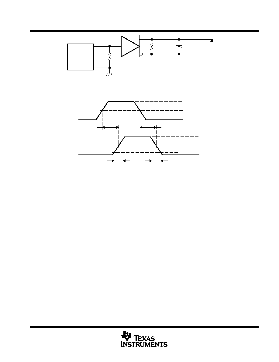
PARAMETER MEASUREMENT INFORMATION
GND
VI
A
IOZ
IOY
Y
Z
VOD
VOY
II
VOZ
54
Figure 1. Test Circuit, V
OD
Without Common-Mode Loading
375
VTEST = ≠7 V to 12 V
Y
Z
VOD
Input
60
375
VI
A
VTEST
Figure 2. Test Circuit, V
OD
With Common-Mode Loading
Y
Z
VOC
27
A
50
Signal
Generator
CL = 50 pF
27
PRR = 1 MHz, 50% duty cycle, tr < 6 ns, tf < 6 ns, ZO = 50
Includes probe and jig capacitance
Figure 3. V
OC
Test Circuit
SN65LBC172A, SN75LBC172A
QUADRUPLE RS-485 DIFFERENTIAL LINE DRIVERS
SLLS447B ≠ OCTOBER 2000 ≠ REVISED MAY 2003
7
POST OFFICE BOX 655303
∑
DALLAS, TEXAS 75265
Y
Z
VOD
RL = 54
A
50
Signal
Generator
CL = 50 pF
90%
Output
0 V
10%
tf
≠1.5 V
1.5 V
tr
Input
0 V
3 V
tPHL
1.5 V
tPLH
PRR = 1 MHz, 50% duty cycle, tr < 6 ns, tf < 6 ns, ZO = 50
Includes probe and jig capacitance
Figure 4. Output Switching Test Circuit and Waveforms

SN65LBC172A, SN75LBC172A
QUADRUPLE RS-485 DIFFERENTIAL LINE DRIVERS
SLLS447B ≠ OCTOBER 2000 ≠ REVISED MAY 2003
8
POST OFFICE BOX 655303
∑
DALLAS, TEXAS 75265
PARAMETER MEASUREMENT INFORMATION
S1
A
50
Signal
Generator
Output
2.3 V
Input
0 V
3 V
1.5 V
tPZH
0.5 V
0 V
VOH
tPHZ
0 V or 3 V
w
Input
G
G
RL = 110
CL = 50 pF
Output
3 V
Y
Z
PRR = 1 MHz, 50% duty cycle, tr < 6 ns, tf < 6 ns, ZO = 50
Includes probe and jig capacitance
ß 3-V if testing Y output, 0 V if testing Z output
Figure 5. Enable Timing Test Circuit and Waveforms, t
PZH
and t
PHZ

SN65LBC172A, SN75LBC172A
QUADRUPLE RS-485 DIFFERENTIAL LINE DRIVERS
SLLS447B ≠ OCTOBER 2000 ≠ REVISED MAY 2003
9
POST OFFICE BOX 655303
∑
DALLAS, TEXAS 75265
PARAMETER MEASUREMENT INFORMATION
S1
A
50
Signal
Generator
Output
2.3 V
Input
0 V
3 V
1.5 V
tPZL
0.5 V
5 V
VOL
tPLZ
0 V or 3 V
w
Input
G
G
RL = 110
CL = 50 pF
Output
3 V
5 V
Y
Z
PRR = 1 MHz, 50% duty cycle, tr < 6 ns, tf < 6 ns, ZO = 50
Includes probe and jig capacitance
ß 3-V if testing Y output, 0 V if testing Z output
Figure 6. Enable Timing Test Circuit and Waveforms, t
PZL
and t
PLZ
SN65LBC172A, SN75LBC172A
QUADRUPLE RS-485 DIFFERENTIAL LINE DRIVERS
SLLS447B ≠ OCTOBER 2000 ≠ REVISED MAY 2003
10
POST OFFICE BOX 655303
∑
DALLAS, TEXAS 75265
Voltage Source
VTEST = ≠7 V to 12 V
Slew Rate
1.2 V/
µ
s
VI
VTEST
IO
Y
Z
Figure 7. Test Circuit, Short-Circuit Output Current
VTEST
Pulse Generator
15
µ
s Duration,
1% Duty Cycle
100
Y
Z
≠VTEST
15
µ
s
1.5 ms
0 V
Figure 8. Test Circuit and Waveform, Transient Over-Voltage
SN65LBC172A, SN75LBC172A
QUADRUPLE RS-485 DIFFERENTIAL LINE DRIVERS
SLLS447B ≠ OCTOBER 2000 ≠ REVISED MAY 2003
11
POST OFFICE BOX 655303
∑
DALLAS, TEXAS 75265
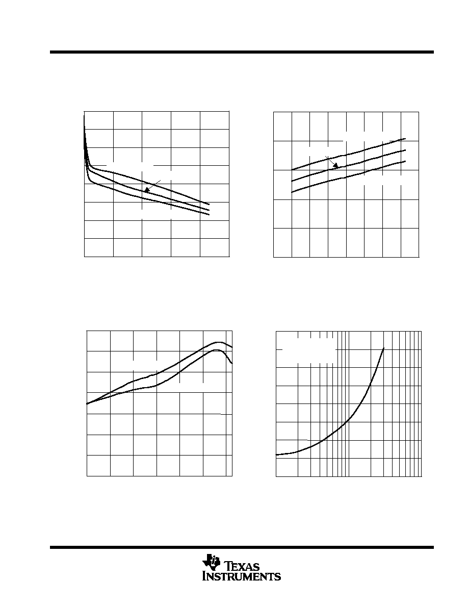
TYPICAL CHARACTERISTICS
Figure 9
0
0.5
1
1.5
2
2.5
3
3.5
4
0
20
40
60
80
100
VCC = 5.25 V
VCC = 5 V
VCC = 4.75 V
≠
Differential Output V
oltage
≠
V
DIFFERENTIAL OUTPUT VOLTAGE
vs
OUTPUT CURRENT
IO ≠ Output Current ≠ mA
V
OD
Figure 10
0
0.5
1
1.5
2
2.5
≠60
≠40
≠20
0
20
40
60
80
100
VCC = 5.25 V
VCC = 5 V
VCC = 4.75 V
≠
Differential Output V
oltage
≠
V
DIFFERENTIAL OUTPUT VOLTAGE
vs
FREE-AIR TEMPERATURE
V
OD
TA ≠ Free-Air Temperature ≠
∞
C
Figure 11
5
5.5
6
6.5
7
7.5
8
8.5
≠40
≠20
0
20
40
60
80
VCC = 5.25 V
VCC = 4.75 V
Propigation Delay T
ime
≠
ns
PROPAGATION DELAY TIME
vs
TEMPERATURE
T ≠ Temperature ≠
∞
C
Figure 12
128
130
132
134
136
138
140
142
144
1
10
100
≠
Supply Current (Four Channels)
≠
mA
Signaling Rate ≠ Mbps
SUPPLY CURRENT (FOUR CHANNELS)
vs
SIGNALING RATE
I CC
RL = 54
CL = 50 pF
(Each Channel)

SN65LBC172A, SN75LBC172A
QUADRUPLE RS-485 DIFFERENTIAL LINE DRIVERS
SLLS447B ≠ OCTOBER 2000 ≠ REVISED MAY 2003
12
POST OFFICE BOX 655303
∑
DALLAS, TEXAS 75265
TYPICAL CHARACTERISTICS
RL = 54
CL = 50 pF
Figure 13. Eye Pattern, Pseudorandom Data at 30 Mbps
APPLICATION INFORMATION
TMS320F243
DSP
(Controller)
SPISIMO
SN65LBC172A
SN65LBC175A
TMS320F241
DSP
(Embedded
Application)
SPISIMO
IOPA1
SPISTE
SPISTE
IOPA0
(Handshake
/Status)
SPICLK
IOPA0
IOPA1
(Enable)
SPICLK
SPISOMI
SPISOMI
IOPA2
Figure 14. Typical Application Circuit, DSP-to-DSP Link via Serial Peripheral Interface
SN65LBC172A, SN75LBC172A
QUADRUPLE RS-485 DIFFERENTIAL LINE DRIVERS
SLLS447B ≠ OCTOBER 2000 ≠ REVISED MAY 2003
13
POST OFFICE BOX 655303
∑
DALLAS, TEXAS 75265
MECHANICAL DATA
DW (R-PDSO-G**)
PLASTIC SMALL-OUTLINE PACKAGE
16 PINS SHOWN
4040000 / D 01/00
Seating Plane
0.400 (10,15)
0.419 (10,65)
0.104 (2,65) MAX
1
0.012 (0,30)
0.004 (0,10)
A
8
16
0.020 (0,51)
0.014 (0,35)
0.291 (7,39)
0.299 (7,59)
9
0.010 (0,25)
0.050 (1,27)
0.016 (0,40)
(15,24)
(15,49)
PINS **
0.010 (0,25) NOM
A MAX
DIM
A MIN
Gage Plane
20
0.500
(12,70)
(12,95)
0.510
(10,16)
(10,41)
0.400
0.410
16
0.600
24
0.610
(17,78)
28
0.700
(18,03)
0.710
0.004 (0,10)
M
0.010 (0,25)
0.050 (1,27)
0
∞
≠ 8
∞
NOTES: A. All linear dimensions are in inches (millimeters).
B. This drawing is subject to change without notice.
C. Body dimensions do not include mold flash or protrusion not to exceed 0.006 (0,15).
D. Falls within JEDEC MS-013

SN65LBC172A, SN75LBC172A
QUADRUPLE RS-485 DIFFERENTIAL LINE DRIVERS
SLLS447B ≠ OCTOBER 2000 ≠ REVISED MAY 2003
14
POST OFFICE BOX 655303
∑
DALLAS, TEXAS 75265
MECHANICAL DATA
N (R-PDIP-T**)
PLASTIC DUAL-IN-LINE PACKAGE
0.325 (8,26)
0.300 (7,62)
0.010 (0,25) NOM
Gauge Plane
0.015 (0,38)
0.430 (10,92) MAX
20
0.975
(24,77)
0.940
(23,88)
18
0.920
0.850
14
0.775
0.745
(19,69)
(18,92)
16
0.775
(19,69)
(18,92)
0.745
A MIN
DIM
A MAX
PINS **
(23,37)
(21,59)
Seating Plane
14/18 PIN ONLY
4040049/D 02/00
9
8
0.070 (1,78) MAX
A
0.035 (0,89) MAX
0.020 (0,51) MIN
16
1
0.015 (0,38)
0.021 (0,53)
0.200 (5,08) MAX
0.125 (3,18) MIN
0.240 (6,10)
0.260 (6,60)
M
0.010 (0,25)
0.100 (2,54)
16 PINS SHOWN
NOTES: A. All linear dimensions are in inches (millimeters).
B. This drawing is subject to change without notice.
C. Falls within JEDEC MS-001 (20-pin package is shorter than MS-001).

PACKAGING INFORMATION
Orderable Device
Status
(1)
Package
Type
Package
Drawing
Pins Package
Qty
Eco Plan
(2)
Lead/Ball Finish
MSL Peak Temp
(3)
SN65LBC172A16DW
ACTIVE
SOIC
DW
16
40
TBD
CU NIPDAU
Level-1-220C-UNLIM
SN65LBC172A16DWR
ACTIVE
SOIC
DW
16
2000
TBD
CU NIPDAU
Level-1-220C-UNLIM
SN65LBC172ADW
ACTIVE
SOIC
DW
20
25
TBD
CU NIPDAU
Level-1-220C-UNLIM
SN65LBC172ADWR
ACTIVE
SOIC
DW
20
2000
TBD
CU NIPDAU
Level-1-220C-UNLIM
SN65LBC172AN
ACTIVE
PDIP
N
16
25
TBD
CU NIPD
N / A for Pkg Type
SN75LBC172A16DW
ACTIVE
SOIC
DW
16
40
TBD
CU NIPDAU
Level-1-220C-UNLIM
SN75LBC172A16DWR
ACTIVE
SOIC
DW
16
2000
TBD
CU NIPDAU
Level-1-220C-UNLIM
SN75LBC172ADW
ACTIVE
SOIC
DW
20
25
TBD
CU NIPDAU
Level-1-220C-UNLIM
SN75LBC172ADWR
ACTIVE
SOIC
DW
20
2000
TBD
CU NIPDAU
Level-1-220C-UNLIM
SN75LBC172AN
ACTIVE
PDIP
N
16
25
TBD
CU NIPD
N / A for Pkg Type
(1)
The marketing status values are defined as follows:
ACTIVE: Product device recommended for new designs.
LIFEBUY: TI has announced that the device will be discontinued, and a lifetime-buy period is in effect.
NRND: Not recommended for new designs. Device is in production to support existing customers, but TI does not recommend using this part in
a new design.
PREVIEW: Device has been announced but is not in production. Samples may or may not be available.
OBSOLETE: TI has discontinued the production of the device.
(2)
Eco Plan - The planned eco-friendly classification: Pb-Free (RoHS), Pb-Free (RoHS Exempt), or Green (RoHS & no Sb/Br) - please check
http://www.ti.com/productcontent
for the latest availability information and additional product content details.
TBD: The Pb-Free/Green conversion plan has not been defined.
Pb-Free (RoHS): TI's terms "Lead-Free" or "Pb-Free" mean semiconductor products that are compatible with the current RoHS requirements
for all 6 substances, including the requirement that lead not exceed 0.1% by weight in homogeneous materials. Where designed to be soldered
at high temperatures, TI Pb-Free products are suitable for use in specified lead-free processes.
Pb-Free (RoHS Exempt): This component has a RoHS exemption for either 1) lead-based flip-chip solder bumps used between the die and
package, or 2) lead-based die adhesive used between the die and leadframe. The component is otherwise considered Pb-Free (RoHS
compatible) as defined above.
Green (RoHS & no Sb/Br): TI defines "Green" to mean Pb-Free (RoHS compatible), and free of Bromine (Br) and Antimony (Sb) based flame
retardants (Br or Sb do not exceed 0.1% by weight in homogeneous material)
(3)
MSL, Peak Temp. -- The Moisture Sensitivity Level rating according to the JEDEC industry standard classifications, and peak solder
temperature.
Important Information and Disclaimer:The information provided on this page represents TI's knowledge and belief as of the date that it is
provided. TI bases its knowledge and belief on information provided by third parties, and makes no representation or warranty as to the
accuracy of such information. Efforts are underway to better integrate information from third parties. TI has taken and continues to take
reasonable steps to provide representative and accurate information but may not have conducted destructive testing or chemical analysis on
incoming materials and chemicals. TI and TI suppliers consider certain information to be proprietary, and thus CAS numbers and other limited
information may not be available for release.
In no event shall TI's liability arising out of such information exceed the total purchase price of the TI part(s) at issue in this document sold by TI
to Customer on an annual basis.
PACKAGE OPTION ADDENDUM
www.ti.com
12-Jan-2006
Addendum-Page 1


IMPORTANT NOTICE
Texas Instruments Incorporated and its subsidiaries (TI) reserve the right to make corrections, modifications,
enhancements, improvements, and other changes to its products and services at any time and to discontinue
any product or service without notice. Customers should obtain the latest relevant information before placing
orders and should verify that such information is current and complete. All products are sold subject to TI's terms
and conditions of sale supplied at the time of order acknowledgment.
TI warrants performance of its hardware products to the specifications applicable at the time of sale in
accordance with TI's standard warranty. Testing and other quality control techniques are used to the extent TI
deems necessary to support this warranty. Except where mandated by government requirements, testing of all
parameters of each product is not necessarily performed.
TI assumes no liability for applications assistance or customer product design. Customers are responsible for
their products and applications using TI components. To minimize the risks associated with customer products
and applications, customers should provide adequate design and operating safeguards.
TI does not warrant or represent that any license, either express or implied, is granted under any TI patent right,
copyright, mask work right, or other TI intellectual property right relating to any combination, machine, or process
in which TI products or services are used. Information published by TI regarding third-party products or services
does not constitute a license from TI to use such products or services or a warranty or endorsement thereof.
Use of such information may require a license from a third party under the patents or other intellectual property
of the third party, or a license from TI under the patents or other intellectual property of TI.
Reproduction of information in TI data books or data sheets is permissible only if reproduction is without
alteration and is accompanied by all associated warranties, conditions, limitations, and notices. Reproduction
of this information with alteration is an unfair and deceptive business practice. TI is not responsible or liable for
such altered documentation.
Resale of TI products or services with statements different from or beyond the parameters stated by TI for that
product or service voids all express and any implied warranties for the associated TI product or service and
is an unfair and deceptive business practice. TI is not responsible or liable for any such statements.
Following are URLs where you can obtain information on other Texas Instruments products and application
solutions:
Products
Applications
Amplifiers
amplifier.ti.com
Audio
www.ti.com/audio
Data Converters
dataconverter.ti.com
Automotive
www.ti.com/automotive
DSP
dsp.ti.com
Broadband
www.ti.com/broadband
Interface
interface.ti.com
Digital Control
www.ti.com/digitalcontrol
Logic
logic.ti.com
Military
www.ti.com/military
Power Mgmt
power.ti.com
Optical Networking
www.ti.com/opticalnetwork
Microcontrollers
microcontroller.ti.com
Security
www.ti.com/security
Telephony
www.ti.com/telephony
Video & Imaging
www.ti.com/video
Wireless
www.ti.com/wireless
Mailing Address:
Texas Instruments
Post Office Box 655303 Dallas, Texas 75265
Copyright 2006, Texas Instruments Incorporated