SN54ABT16601, SN74ABT16601
18-BIT UNIVERSAL BUS TRANSCEIVERS
WITH 3-STATE OUTPUTS
SCBS210C ≠ JUNE 1992 ≠ REVISED JANUARY 1997
1
POST OFFICE BOX 655303
∑
DALLAS, TEXAS 75265
D
Members of the Texas Instruments
Widebus
TM
Family
D
State-of-the-Art
EPIC-
B
TM
BiCMOS Design
Significantly Reduces Power Dissipation
D
UBT
TM
(Universal Bus Transceiver)
Combines D-Type Latches and D-Type
Flip-Flops for Operation in Transparent,
Latched, Clocked, or Clock-Enabled Mode
D
Latch-Up Performance Exceeds 500 mA Per
JEDEC Standard JESD-17
D
Typical V
OLP
(Output Ground Bounce)
< 0.8 V at V
CC
= 5 V, T
A
= 25
∞
C
D
Flow-Through Architecture Optimizes PCB
Layout
D
Package Options Include Plastic 300-mil
Shrink Small-Outline (DL) and Thin Shrink
Small-Outline (DGG) Packages and 380-mil
Fine-Pitch Ceramic Flat (WD) Package
Using 25-mil Center-to-Center Spacings
description
These 18-bit universal bus transceivers combine
D-type latches and D-type flip-flops to allow data
flow in transparent, latched, clocked, and
clock-enabled modes.
Data flow in each direction is controlled by
output-enable (OEAB and OEBA), latch-enable
(LEAB and LEBA), and clock (CLKAB and
CLKBA) inputs. The clock can be controlled by the
clock-enable (CLKENAB and CLKENBA) inputs.
For A-to-B data flow, the device operates in the
transparent mode when LEAB is high. When
LEAB is low, the A data is latched if CLKAB is held
at a high or low logic level. If LEAB is low, the
A data is stored in the latch/flip-flop on the
low-to-high transition of CLKAB. Output enable
OEAB is active low. When OEAB is low, the
outputs are active. When OEAB is high, the
outputs are in the high-impedance state.
Data flow for B to A is similar to that of A to B, but uses OEBA, LEBA, CLKBA, and CLKENBA.
To ensure the high-impedance state during power up or power down, OE should be tied to V
CC
through a pullup
resistor; the minimum value of the resistor is determined by the current-sinking capability of the driver.
The SN54ABT16601 is characterized for operation over the full military temperature range of ≠55
∞
C to 125
∞
C.
The SN74ABT16601 is characterized for operation from ≠40
∞
C to 85
∞
C.
Copyright
©
1997, Texas Instruments Incorporated
PRODUCTION DATA information is current as of publication date.
Products conform to specifications per the terms of Texas Instruments
standard warranty. Production processing does not necessarily include
testing of all parameters.
Please be aware that an important notice concerning availability, standard warranty, and use in critical applications of
Texas Instruments semiconductor products and disclaimers thereto appears at the end of this data sheet.
Widebus, EPIC-
B, and UBT are trademarks of Texas Instruments Incorporated.
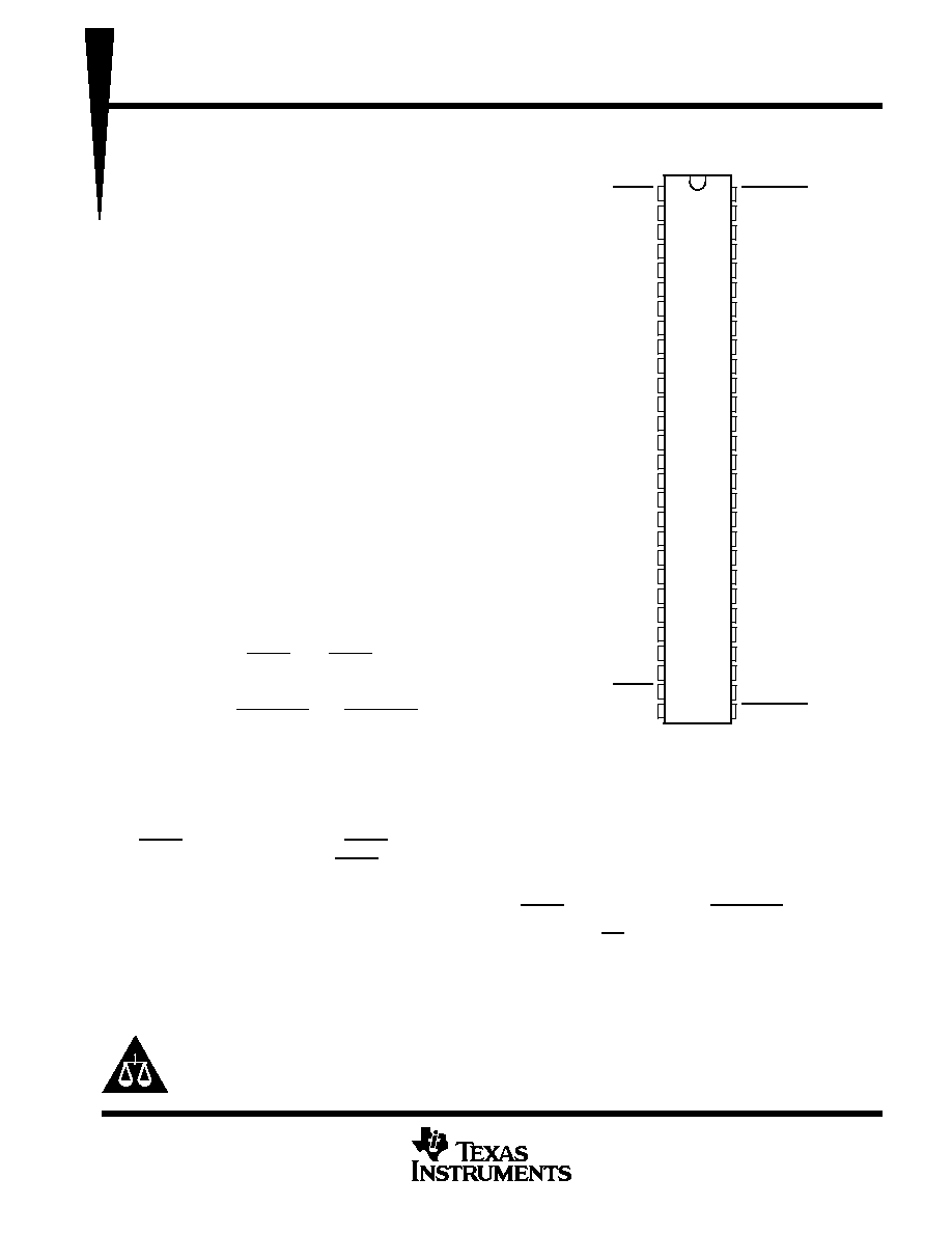
SN54ABT16601 . . . WD PACKAGE
SN74ABT16601 . . . DGG OR DL PACKAGE
(TOP VIEW)
1
2
3
4
5
6
7
8
9
10
11
12
13
14
15
16
17
18
19
20
21
22
23
24
25
26
27
28
56
55
54
53
52
51
50
49
48
47
46
45
44
43
42
41
40
39
38
37
36
35
34
33
32
31
30
29
OEAB
LEAB
A1
GND
A2
A3
V
CC
A4
A5
A6
GND
A7
A8
A9
A10
A11
A12
GND
A13
A14
A15
V
CC
A16
A17
GND
A18
OEBA
LEBA
CLKENAB
CLKAB
B1
GND
B2
B3
V
CC
B4
B5
B6
GND
B7
B8
B9
B10
B11
B12
GND
B13
B14
B15
V
CC
B16
B17
GND
B18
CLKBA
CLKENBA
SN54ABT16601, SN74ABT16601
18-BIT UNIVERSAL BUS TRANSCEIVERS
WITH 3-STATE OUTPUTS
SCBS210C ≠ JUNE 1992 ≠ REVISED JANUARY 1997
2
POST OFFICE BOX 655303
∑
DALLAS, TEXAS 75265
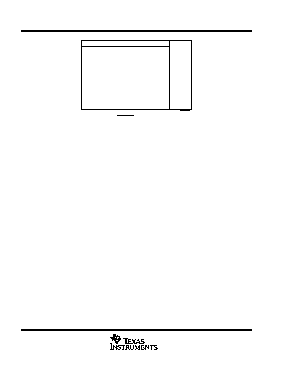
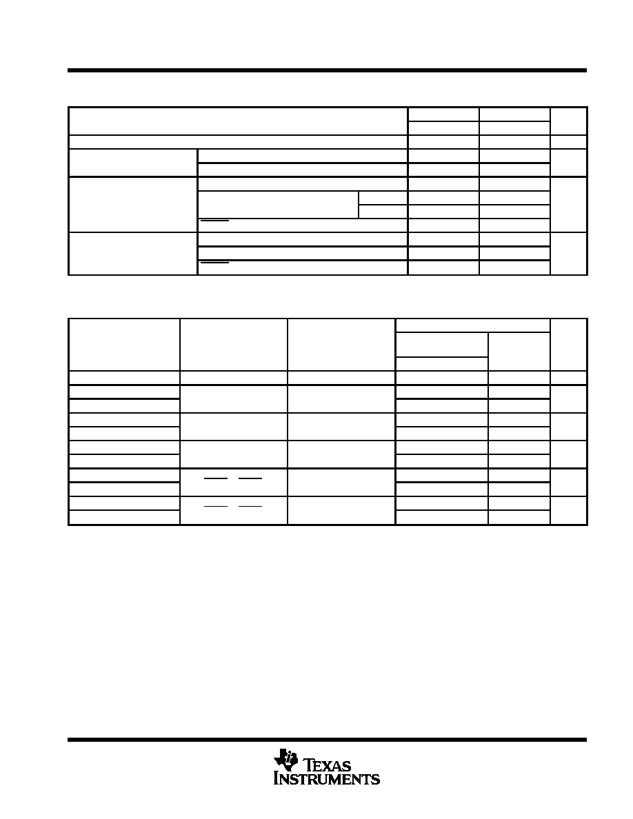
FUNCTION TABLE
INPUTS
OUTPUT
CLKENAB
OEAB
LEAB
CLKAB
A
B
X
H
X
X
X
Z
X
L
H
X
L
L
X
L
H
X
H
H
H
L
L
X
X
B0
H
L
L
X
X
B0
L
L
L
L
L
L
L
L
H
H
L
L
L
L
X
B0
L
L
L
H
X
B0ß
A-to-B data flow is shown: B-to-A flow is similar but uses OEBA,
LEBA, CLKBA, and CLKENBA.
Output level before the indicated steady-state input conditions were
established
ß Output level before the indicated steady-state input conditions were
established, provided that CLKAB was low before LEAB went low
SN54ABT16601, SN74ABT16601
18-BIT UNIVERSAL BUS TRANSCEIVERS
WITH 3-STATE OUTPUTS
SCBS210C ≠ JUNE 1992 ≠ REVISED JANUARY 1997
3
POST OFFICE BOX 655303
∑
DALLAS, TEXAS 75265
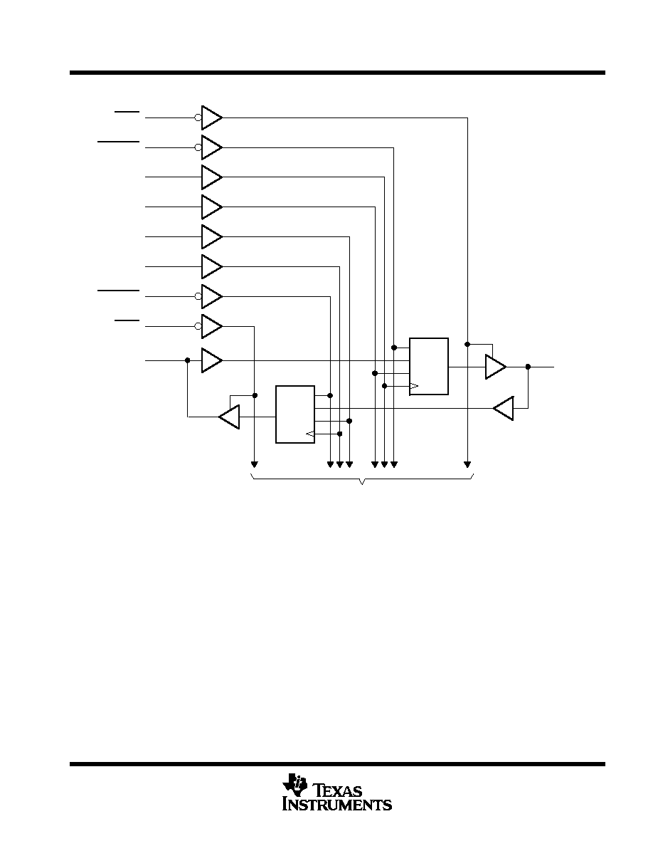
logic diagram (positive logic)
CE
1D
C1
CLK
CE
1D
C1
CLK
B1
OEAB
CLKENAB
CLKAB
LEAB
LEBA
CLKBA
CLKENBA
OEBA
A1
1
56
55
2
28
30
29
27
3
54
To 17 Other Channels
absolute maximum ratings over operating free-air temperature range (unless otherwise noted)
Supply voltage range, V
CC
≠0.5 V to 7 V
. . . . . . . . . . . . . . . . . . . . . . . . . . . . . . . . . . . . . . . . . . . . . . . . . . . . . . . . . .
Input voltage range, V
I
(except I/O ports) (see Note 1)
≠0.5 V to 7 V
. . . . . . . . . . . . . . . . . . . . . . . . . . . . . . . . . .
Voltage range applied to any output in the high or power-off state, V
O
≠0.5 V to 5.5 V
. . . . . . . . . . . . . . . . . . .
Current into any output in the low state, I
O
: SN54ABT16601 96
mA
. . . . . . . . . . . . . . . . . . . . . . . . . . . . . . . . . .
SN74ABT16601 128
mA
. . . . . . . . . . . . . . . . . . . . . . . . . . . . . . . . .
Input clamp current, I
IK
(V
I
< 0)
≠18 mA
. . . . . . . . . . . . . . . . . . . . . . . . . . . . . . . . . . . . . . . . . . . . . . . . . . . . . . . . . . .
Output clamp current, I
OK
(V
O
< 0)
≠50 mA
. . . . . . . . . . . . . . . . . . . . . . . . . . . . . . . . . . . . . . . . . . . . . . . . . . . . . . . .
Package thermal impedance,
JA
(see Note 2): DGG package
81
∞
C/W
. . . . . . . . . . . . . . . . . . . . . . . . . . . . . . .
DL package
74
∞
C/W
. . . . . . . . . . . . . . . . . . . . . . . . . . . . . . . . .
Storage temperature range, T
stg
≠65
∞
C to 150
∞
C
. . . . . . . . . . . . . . . . . . . . . . . . . . . . . . . . . . . . . . . . . . . . . . . . . . .
Stresses beyond those listed under "absolute maximum ratings" may cause permanent damage to the device. These are stress ratings only, and
functional operation of the device at these or any other conditions beyond those indicated under "recommended operating conditions" is not
implied. Exposure to absolute-maximum-rated conditions for extended periods may affect device reliability.
NOTES:
1. The input and output negative-voltage ratings may be exceeded if the input and output clamp-current ratings are observed.
2. The package thermal impedance is calculated in accordance with EIA/JEDEC Std JESD51.
SN54ABT16601, SN74ABT16601
18-BIT UNIVERSAL BUS TRANSCEIVERS
WITH 3-STATE OUTPUTS
SCBS210C ≠ JUNE 1992 ≠ REVISED JANUARY 1997
4
POST OFFICE BOX 655303
∑
DALLAS, TEXAS 75265
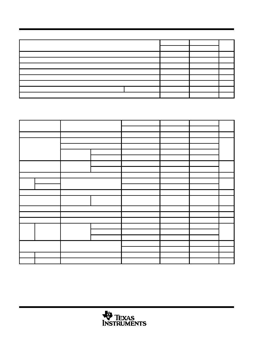
recommended operating conditions (see Note 3)
SN54ABT16601
SN74ABT16601
UNIT
MIN
MAX
MIN
MAX
UNIT
VCC
Supply voltage
4.5
5.5
4.5
5.5
V
VIH
High-level input voltage
2
2
V
VIL
Low-level input voltage
0.8
0.8
V
VI
Input voltage
0
VCC
0
VCC
V
IOH
High-level output current
≠24
≠32
mA
IOL
Low-level output current
48
64
mA
t/
v
Input transition rise or fall rate
Outputs enabled
10
10
ns/V
TA
Operating free-air temperature
≠55
125
≠40
85
∞
C
NOTE 3: Unused pins (input or I/O) must be held high or low to prevent them from floating.
electrical characteristics over recommended operating free-air temperature range (unless
otherwise noted)
PARAMETER
TEST CONDITIONS
TA = 25
∞
C
SN54ABT16601
SN74ABT16601
UNIT
PARAMETER
TEST CONDITIONS
MIN
TYP
MAX
MIN
MAX
MIN
MAX
UNIT
VIK
VCC = 4.5 V,
II = ≠18 mA
≠1.2
≠1.2
≠1.2
V
VCC = 4.5 V,
IOH = ≠3 mA
2.5
2.5
2.5
VOH
VCC = 5 V,
IOH = ≠3 mA
3
3
3
V
VOH
VCC = 4 5 V
IOH = ≠24 mA
2
2
V
VCC = 4.5 V
IOH = ≠32 mA
2*
2
VOL
VCC = 4 5 V
IOL = 48 mA
0.55
0.55
V
VOL
VCC = 4.5 V
IOL = 64 mA
0.55*
0.55
V
Vhys
100
mV
II
Control inputs
VCC = 5 5 V
VI = VCC or GND
±
1
±
1
±
1
µ
A
II
A or B ports
VCC = 5.5 V,
VI = VCC or GND
±
20**
±
100
±
20
µ
A
Ioff
VCC = 0,
VI or VO
4.5 V
±
100
±
100
µ
A
ICEX
VCC = 5.5 V,
VO = 5.5 V
Outputs high
50
50
50
µ
A
IO
VCC = 5.5 V,
VO = 2.5 V
≠50
≠100
≠180
≠50
≠180
≠50
≠180
mA
IOZHß
VCC = 5.5 V,
VO = 2.7 V
10
10
10
µ
A
IOZLß
VCC = 5.5 V,
VO = 0.5 V
≠10
≠10
≠10
µ
A
VCC = 5.5 V,
Outputs high
1.9
3
2
3
ICC
A or B ports
VCC = 5.5 V,
IO = 0,
Outputs low
28
36
35
36
mA
VI = VCC or GND Outputs disabled
1.6
3
2
3
I
∂
VCC = 5.5 V, One input at 3.4 V,
50
50
µ
A
ICC∂
CC
,
,
Other inputs at VCC or GND
1.5
mA
Ci
Control inputs
VI = 2.5 V or 0.5 V
3
pF
Cio
A or B ports
VO = 2.5 V or 0.5 V
9
pF
* On products compliant to MIL-PRF-38535, this parameter does not apply.
** This limit applies only to the SN74ABT16601.
All typical values are at VCC = 5 V.
Not more than one output should be tested at a time, and the duration of the test should not exceed one second.
ß The parameters IOZH and IOZL include the input leakage current.
∂ This is the increase in supply current for each input that is at the specified TTL voltage level rather than VCC or GND.
SN54ABT16601, SN74ABT16601
18-BIT UNIVERSAL BUS TRANSCEIVERS
WITH 3-STATE OUTPUTS
SCBS210C ≠ JUNE 1992 ≠ REVISED JANUARY 1997
5
POST OFFICE BOX 655303
∑
DALLAS, TEXAS 75265
timing requirements over recommended ranges of supply voltage and operating free-air
temperature (unless otherwise noted) (see Figure 1)
SN54ABT16601
SN74ABT16601
UNIT
MIN
MAX
MIN
MAX
UNIT
fclock
Clock frequency
0
150
0
150
MHz
t
Pulse duration
LEAB or LEBA high
2.5
2.5
ns
tw
Pulse duration
CLKAB or CLKBA high or low
3
3
ns
A before CLKAB
or B before CLKBA
4.6
4
t
Setup time
A before LEAB
or B before LEBA
CLK high
2.5
2.5
ns
tsu
Setup time
A before LEAB
or B before LEBA
CLK low
1.3
1
ns
CLKEN before CLK
2.9
2.5
A after CLKAB
or B after CLKBA
0.4
0
th
Hold time
A after LEAB
or B after LEBA
2.8
2
ns
CLKEN after CLK
0
0
switching characteristics over recommended ranges of supply voltage and operating free-air
temperature, C
L
= 50 pF (unless otherwise noted) (see Figure 1)
SN54ABT16601
PARAMETER
FROM
(INPUT)
TO
(OUTPUT)
VCC = 5 V,
TA = 25
∞
C
MIN
MAX
UNIT
MIN
TYP
MAX
fmax
150
200
150
MHz
tPLH
A or B
B or A
1.5
2.5
4.1
1
4.6
ns
tPHL
A or B
B or A
1.5
3.4
4.7
1
5.1
ns
tPLH
LEAB or LEBA
B or A
2
3.4
4.7
1
5.6
ns
tPHL
LEAB or LEBA
B or A
2
3.7
5
1
5.5
ns
tPLH
CLKAB or CLKBA
B or A
1.5
3.2
4.5
1
5.2
ns
tPHL
CLKAB or CLKBA
B or A
1.5
3.2
4.4
1
5
ns
tPZH
OEAB or OEBA
B or A
2
4
5
1
5.7
ns
tPZL
OEAB or OEBA
B or A
2
4.2
5.6
1
6
ns
tPHZ
OEAB or OEBA
B or A
2
4.5
5.8
1
6.8
ns
tPLZ
OEAB or OEBA
B or A
1.5
3.4
5.3
1
6.3
ns