
SN54AC244, SN74AC244
OCTAL BUFFERS/DRIVERS
WITH 3-STATE OUTPUTS
SCAS514C ≠ JUNE 1995 ≠ REVISED SEPTEMBER 1996
1
POST OFFICE BOX 655303
∑
DALLAS, TEXAS 75265
D
EPIC
TM
(Enhanced-Performance Implanted
CMOS) 1-
µ
m Process
D
Package Options Include Plastic
Small-Outline (DW), Shrink Small-Outline
(DB), and Thin Shrink Small-Outline (PW)
Packages, Ceramic Chip Carriers (FK), Flat
(W), and DIP (J, N) Packages
description
These octal buffers and line drivers are designed
specifically to improve the performance and
density of 3-state memory address drivers, clock
drivers, and bus-oriented receivers and
transmitters.
The 'AC244 are organized as two 4-bit
buffers/drivers with separate output-enable (OE)
inputs. When OE is low, the device passes
noninverted data from the A inputs to the Y
outputs. When OE is high, the outputs are in the
high-impedance state.
The SN54AC244 is characterized for operation
over the full military temperature range of ≠55
∞
C
to 125
∞
C. The SN74AC244 is characterized for
operation from ≠40
∞
C to 85
∞
C.
FUNCTION TABLE
(each buffer)
INPUTS
OUTPUT
OE
A
Y
L
H
H
L
L
L
H
X
Z
Copyright
©
1996, Texas Instruments Incorporated
PRODUCTION DATA information is current as of publication date.
Products conform to specifications per the terms of Texas Instruments
standard warranty. Production processing does not necessarily include
testing of all parameters.
Please be aware that an important notice concerning availability, standard warranty, and use in critical applications of
Texas Instruments semiconductor products and disclaimers thereto appears at the end of this data sheet.
EPIC is a trademark of Texas Instruments Incorporated.
SN54AC244 . . . J OR W PACKAGE
SN74AC244 . . . DB, DW, N, OR PW PACKAGE
(TOP VIEW)
3
2
1 20 19
9 10 11 12 13
4
5
6
7
8
18
17
16
15
14
1Y1
2A4
1Y2
2A3
1Y3
1A2
2Y3
1A3
2Y2
1A4
SN54AC244 . . . FK PACKAGE
(TOP VIEW)
2Y4
1A1
1OE
1Y4
2A2
2OE
2Y1
GND
2A1
V
CC
1
2
3
4
5
6
7
8
9
10
20
19
18
17
16
15
14
13
12
11
1OE
1A1
2Y4
1A2
2Y3
1A3
2Y2
1A4
2Y1
GND
V
CC
2OE
1Y1
2A4
1Y2
2A3
1Y3
2A2
1Y4
2A1
SN54AC244, SN74AC244
OCTAL BUFFERS/DRIVERS
WITH 3-STATE OUTPUTS
SCAS514C ≠ JUNE 1995 ≠ REVISED SEPTEMBER 1996
2
POST OFFICE BOX 655303
∑
DALLAS, TEXAS 75265
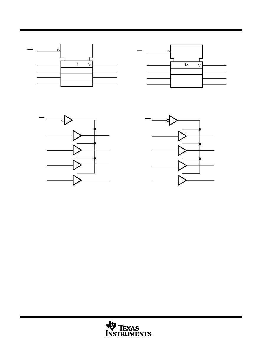
logic symbol
2
1A1
4
1A2
6
1A3
8
1A4
EN
1
1Y1
18
1Y2
16
1Y3
14
1Y4
12
11
2A1
13
2A2
15
2A3
17
2A4
EN
19
2Y1
9
2Y2
7
2Y3
5
2Y4
3
1OE
2OE
This symbol is in accordance with ANSI/IEEE Std 91-1984 and IEC Publication 617-12.
logic diagram (positive Logic)
1
2
4
6
8
12
14
16
18
1A1
1A2
1A3
1A4
1Y1
1Y2
1Y3
1Y4
1OE
19
11
13
15
17
3
5
7
9
2A1
2A2
2A3
2A4
2Y1
2Y2
2Y3
2Y4
2OE
absolute maximum ratings over operating free-air temperature range (unless otherwise noted)
Supply voltage range, V
CC
≠0.5 V to 7 V
. . . . . . . . . . . . . . . . . . . . . . . . . . . . . . . . . . . . . . . . . . . . . . . . . . . . . . . . . .
Input voltage range, V
I
(see Note 1)
≠0.5 V to V
CC
+ 0.5 V
. . . . . . . . . . . . . . . . . . . . . . . . . . . . . . . . . . . . . . . . . . .
Output voltage range, V
O
(see Note 1)
≠0.5 V to V
CC
+ 0.5 V
. . . . . . . . . . . . . . . . . . . . . . . . . . . . . . . . . . . . . . . .
Input clamp current, I
IK
(V
I
< 0 or V
I
> V
CC
)
±
20 mA
. . . . . . . . . . . . . . . . . . . . . . . . . . . . . . . . . . . . . . . . . . . . . . . .
Output clamp current, I
OK
(V
O
< 0 or V
O
> V
CC
)
±
20 mA
. . . . . . . . . . . . . . . . . . . . . . . . . . . . . . . . . . . . . . . . . . . .
Continuous output current, I
O
(V
O
= 0 to V
CC
)
±
50 mA
. . . . . . . . . . . . . . . . . . . . . . . . . . . . . . . . . . . . . . . . . . . . . .
Continuous current through V
CC
or GND
±
200 mA
. . . . . . . . . . . . . . . . . . . . . . . . . . . . . . . . . . . . . . . . . . . . . . . . . .
Maximum power dissipation at T
A
= 55
∞
C (in still air) (see Note 2): DB package
0.6 W
. . . . . . . . . . . . . . . . . .
DW package
1.6 W
. . . . . . . . . . . . . . . . . .
N package
1.3 W
. . . . . . . . . . . . . . . . . . . .
PW package
0.7 W
. . . . . . . . . . . . . . . . . .
Storage temperature range, T
stg
≠65
∞
C to 150
∞
C
. . . . . . . . . . . . . . . . . . . . . . . . . . . . . . . . . . . . . . . . . . . . . . . . . . .
Stresses beyond those listed under "absolute maximum ratings" may cause permanent damage to the device. These are stress ratings only, and
functional operation of the device at these or any other conditions beyond those indicated under "recommended operating conditions" is not
implied. Exposure to absolute-maximum-rated conditions for extended periods may affect device reliability.
NOTES:
1. The input and output voltage ratings may be exceeded if the input and output current ratings are observed.
2. The maximum package power dissipation is calculated using a junction temperature of 150
∞
C and a board trace length of 750 mils,
except for the N package, which has a trace length of zero.

SN54AC244, SN74AC244
OCTAL BUFFERS/DRIVERS
WITH 3-STATE OUTPUTS
SCAS514C ≠ JUNE 1995 ≠ REVISED SEPTEMBER 1996
3
POST OFFICE BOX 655303
∑
DALLAS, TEXAS 75265
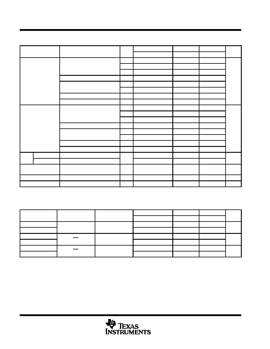
recommended operating conditions (see Note 3)
SN54AC244
SN74AC244
UNIT
MIN
MAX
MIN
MAX
UNIT
VCC
Supply voltage
2
6
2
6
V
VCC = 3 V
2.1
2.1
VIH
High-level input voltage
VCC = 4.5 V
3.15
3.15
V
VCC = 5.5 V
3.85
3.85
VCC = 3 V
0.9
0.9
VIL
Low-level input voltage
VCC = 4.5 V
1.35
1.35
V
VCC = 5.5 V
1.65
1.65
VI
Input voltage
0
VCC
0
VCC
V
VO
Output voltage
0
VCC
0
VCC
V
VCC = 3 V
≠12
≠12
IOH
High-level output current
VCC = 4.5 V
≠24
≠24
mA
VCC = 5.5 V
≠24
≠24
VCC = 3 V
12
12
IOL
Low-level output current
VCC = 4.5 V
24
24
mA
VCC = 5.5 V
24
24
t/
v
Input transition rise or fall rate
0
8
0
8
ns/V
TA
Operating free-air temperature
≠55
125
≠40
85
∞
C
NOTE 3: Unused inputs must be held high or low to prevent them from floating.
SN54AC244, SN74AC244
OCTAL BUFFERS/DRIVERS
WITH 3-STATE OUTPUTS
SCAS514C ≠ JUNE 1995 ≠ REVISED SEPTEMBER 1996
4
POST OFFICE BOX 655303
∑
DALLAS, TEXAS 75265
electrical characteristics over recommended operating free-air temperature range (unless
otherwise noted)
PARAMETER
TEST CONDITIONS
VCC
TA = 25
∞
C
SN54AC244
SN74AC244
UNIT
PARAMETER
TEST CONDITIONS
VCC
MIN
TYP
MAX
MIN
MAX
MIN
MAX
UNIT
3 V
2.9
2.9
2.9
IOH = ≠50
µ
A
4.5 V
4.4
4.4
4.4
5.5 V
5.4
5.4
5.4
VOH
IOH = ≠12 mA
3 V
2.56
2.4
2.46
V
VOH
I
24
A
4.5 V
3.86
3.7
3.76
V
IOL = ≠24 mA
5.5 V
4.86
4.7
4.76
IOH = ≠50 mA
5.5 V
3.85
IOH = ≠75 mA
5.5 V
3.85
3 V
0.1
0.1
0.1
IOL = 50
µ
A
4.5 V
0.1
0.1
0.1
5.5 V
0.1
0.1
0.1
VOL
IOL = 12 mA
3 V
0.36
0.5
0.44
V
VOL
IOL = 24 mA
4.5 V
0.36
0.5
0.44
V
IOL = 24 mA
5.5 V
0.36
0.5
0.44
IOL = 50 mA
5.5 V
1.65
IOL = 75 mA
5.5 V
1.65
II
Data inputs
VI = VCC or GND
5 5 V
±
0.1
±
1
±
1
µ
A
II
Control inputs
VI = VCC or GND
5.5 V
±
0.1
±
1
±
1
µ
A
IOZ
VO = VCC or GND,
VI(OE) = VIL or VIH
5.5 V
±
0.25
±
5
±
2.5
µ
A
ICC
VI = VCC or GND,
IO = 0
5.5 V
4
80
40
µ
A
Ci
VI = VCC or GND
5 V
2.5
pF
Not more than one output should be tested at a time, and the duration of the test should not exceed 10 ms.
switching characteristics over recommended operating free-air temperature range,
V
CC
= 3.3 V
±
0.3 V (unless otherwise noted) (see Figure 1)
PARAMETER
FROM
TO
TA = 25
∞
C
SN54AC244
SN74AC244
UNIT
PARAMETER
(INPUT)
(OUTPUT)
MIN
TYP
MAX
MIN
MAX
MIN
MAX
UNIT
tPLH
A
Y
2
6.5
9
1
12.5
1.5
10
ns
tPHL
A
Y
2
6.5
9
1
12
2
10
ns
tPZH
OE
Y
2
6
10.5
1
11.5
1.5
11
ns
tPZL
OE
Y
2.5
7.5
10
1
13
2
11
ns
tPHZ
OE
Y
3
7
10
1
12.5
1.5
10.5
ns
tPLZ
OE
Y
2.5
7.5
10.5
1
13
2.5
11.5
ns

SN54AC244, SN74AC244
OCTAL BUFFERS/DRIVERS
WITH 3-STATE OUTPUTS
SCAS514C ≠ JUNE 1995 ≠ REVISED SEPTEMBER 1996
5
POST OFFICE BOX 655303
∑
DALLAS, TEXAS 75265
switching characteristics over recommended operating free-air temperature range,
V
CC
= 5 V
±
0.5 V (unless otherwise noted) (see Figure 1)
PARAMETER
FROM
TO
TA = 25
∞
C
SN54AC244
SN74AC244
UNIT
PARAMETER
(INPUT)
(OUTPUT)
MIN
TYP
MAX
MIN
MAX
MIN
MAX
UNIT
tPLH
A
Y
1.5
5
7
1
9.5
1
7.5
ns
tPHL
A
Y
1.5
5
7
1
9
1
7.5
ns
tPZH
OE
Y
1.5
5
7
1
9
1.5
8
ns
tPZL
OE
Y
1.5
5.5
8
1
10.5
1.5
8.5
ns
tPHZ
OE
Y
2.5
6.5
9
1
10.5
1
9.5
ns
tPLZ
OE
Y
2
6.5
9
1
11
2
9.5
ns
operating characteristics, V
CC
= 5 V, T
A
= 25
∞
C
PARAMETER
TEST CONDITIONS
TYP
UNIT
Cpd
Power dissipation capacitance per buffer/driver
CL = 50 pF,
f = 1 MHz
45
pF
PARAMETER MEASUREMENT INFORMATION
From Output
Under Test
CL = 50 pF
(see Note A)
LOAD CIRCUIT
S1
2
◊
VCC
500
500
tPLH
tPHL
Output
Control
(low-level
enabling)
Output
Waveform 1
S1 at 2
◊
VCC
(see Note B)
Output
Waveform 2
S1 at Open
(see Note B)
VOL
VOH
tPZL
tPZH
tPLZ
tPHZ
50% VCC
50% VCC
50% VCC
50% VCC
[
VCC
VCC
0 V
50% VCC
50% VCC
VOH
VOL
0 V
50% VCC
VOL + 0.3 V
50% VCC
VOH ≠ 0.3 V
[
0 V
VCC
Open
Input
Output
VOLTAGE WAVEFORMS
VOLTAGE WAVEFORMS
tPLH/tPHL
tPLZ/tPZL
tPHZ/tPZH
Open
2
◊
VCC
Open
TEST
S1
NOTES: A. CL includes probe and jig capacitance.
B. Waveform 1 is for an output with internal conditions such that the output is low except when disabled by the output control.
Waveform 2 is for an output with internal conditions such that the output is high except when disabled by the output control.
C. All input pulses are supplied by generators having the following characteristics: PRR
1 MHz, ZO = 50
, tr
2.5 ns, tf
2.5 ns.
D. The outputs are measured one at a time with one input transition per measurement.
Figure 1. Load Circuit and Voltage Waveforms