
SN54ACT8990, SN74ACT8990
TEST-BUS CONTROLLERS
IEEE STD 1149.1 (JTAG) TAP MASTERS WITH 16-BIT GENERIC HOST INTERFACES
SCAS190E ≠ JUNE 1990 ≠ REVISED JANUARY 1997
1
POST OFFICE BOX 655303
∑
DALLAS, TEXAS 75265
D
Members of the Texas Instruments
SCOPE
TM
Family of Testability Products
D
Compatible With the IEEE Standard
1149.1-1990 (JTAG) Test Access Port and
Boundary-Scan Architecture
D
Control Operation of Up to Six Parallel
Target Scan Paths
D
Accommodate Pipeline Delay to Target of
Up to 31 Clock Cycles
D
Scan Data Up to 2
32
Clock Cycles
D
Execute Instructions for Up to 2
32
Clock
Cycles
D
Each Device Includes Four Bidirectional
Event Pins for Additional Test Capability
D
Inputs Are TTL-Voltage Compatible
D
EPIC
TM
(Enhanced-Performance Implanted
CMOS) 1-
µ
m Process
D
Packaged in 44-Pin Plastic Leaded Chip
Carrier (FN), 68-Pin Ceramic Pin Grid Array
(GB), and 68-Pin Ceramic Quad Flat
Packages (HV)
description
The 'ACT8990 test-bus controllers (TBC) are members of the Texas Instruments SCOPE
TM
testability
integrated-circuit family. This family of components supports IEEE Standard 1149.1-1990 (JTAG) boundary
scan to facilitate testing of complex circuit-board assemblies. The 'ACT8990 differ from other SCOPE
TM
integrated circuits. Their function is to control the JTAG serial-test bus rather than being target
boundary -scannable devices.
The required signals of the JTAG serial-test bus ≠ test clock (TCK), test mode select (TMS), test data input (TDI),
and test data output (TDO) can be connected from the TBC to a target device without additional logic. This is
done as a chain of IEEE Standard 1149.1-1990 boundary-scannable components that share the same
serial-test bus. The TBC generates TMS and TDI signals for its target(s), receives TDO signals from its target(s),
and buffers its test clock input (TCKI) to a test clock output (TCKO) for distribution to its target(s). The TMS, TDI,
and TDO signals can be connected to a target directly or via a pipeline, with a retiming delay of up to 31 bits.
Since the TBC can be configured to generate up to six separate TMS signals [TMS (5 ≠ 0)], it can be used to
control up to six target scan paths that are connected in parallel (i.e., sharing common TCK, TDI, and TDO
signals).
While most operations of the TBC are synchronous to TCKI, a test-off (TOFF) input is provided for output control
of the target interface, and a test-reset (TRST) input is provided for hardware/software reset of the TBC. In
addition, four event [EVENT (3 ≠ 0)] I/Os are provided for asynchronous communication to target device(s).
Each event has its own event generation/detection logic, and detected events can be counted by two 16-bit
counters.
The TBC operates under the control of a host microprocessor/microcontroller via the 5-bit address bus
[ADRS (4 ≠ 0)] and the 16-bit read/write data bus [DATA (15 ≠ 0)]. Read (RD) and write (WR) strobes are
implemented such that the critical host-interface timing is independent of the TCKI period. Any one of
24 registers can be addressed for read and/or write operations. In addition to control and status registers, the
TBC contains two command registers, a read buffer, and a write buffer. Status of the TBC is transmitted to the
host via ready (RDY) and interrupt (INT) outputs.
Major commands can be issued by the host to cause the TBC to generate the TMS sequences necessary to
move the target(s) from any stable test-access-port (TAP) controller state to any other stable TAP state, to
execute instructions in the Run-Test/Idle TAP state, or to scan instruction or test data through the target(s). A
32-bit counter can be preset to allow a predetermined number of execution or scan operations.
Serial data that appears at the selected TDI input (TDI1 or TDI0) is transferred into the read buffer, which can
be read by the host to obtain up to 16 bits of the serial-data stream. Serial data that is transmitted from the TDO
output is written by the host to the write buffer.
Copyright
©
1997, Texas Instruments Incorporated
PRODUCTION DATA information is current as of publication date.
Products conform to specifications per the terms of Texas Instruments
standard warranty. Production processing does not necessarily include
testing of all parameters.
SCOPE and EPIC are trademarks of Texas Instruments Incorporated.
Please be aware that an important notice concerning availability, standard warranty, and use in critical applications of
Texas Instruments semiconductor products and disclaimers thereto appears at the end of this data sheet.
On products compliant to MIL-PRF-38535, all parameters are tested
unless otherwise noted. On all other products, production
processing does not necessarily include testing of all parameters.

SN54ACT8990, SN74ACT8990
TEST-BUS CONTROLLERS
IEEE STD 1149.1 (JTAG) TAP MASTERS WITH 16-BIT GENERIC HOST INTERFACES
SCAS190E ≠ JUNE 1990 ≠ REVISED JANUARY 1997
2
POST OFFICE BOX 655303
∑
DALLAS, TEXAS 75265
description (continued)
The SN54ACT8990 is characterized for operation over the full military temperature range of ≠55
∞
C to 125
∞
C.
The SN74ACT8990 is characterized for operation from 0
∞
C to 70
∞
C.
ADRS0
GND
INT
NC
NC
ADRS4
ADRS3
NC
ADRS2
ADRS1
NC
DA
T
A14
NC
DA
T
A15
T
OFF
DA
T
A10
NC
DA
T
A
1
1
DA
T
A12
NC
DA
T
A13
NC
DA
T
A
9
RDY
RD
NC
TDI0
TDI1
NC
NC
WR
TRST
NC
28 29
NC
TMS5/EVENT3
TMS4/EVENT2
NC
TMS3/EVENT1
TMS2/EVENT0
NC
V
CC
GND
TMS1
NC
TMS0
TDO
NC
TCKO
TCKI
NC
60
59
58
57
56
55
54
53
52
51
50
49
48
47
46
45
44
30
10
11
12
13
14
15
16
17
18
19
20
21
22
23
24
25
26
NC
DATA0
DATA1
NC
DATA2
DATA3
NC
DATA4
GND
V
CC
NC
DATA5
DATA6
NC
DATA7
DATA8
NC
31 32 33 34
8
7
6
5
4
9
3
1 68 67
2
35 36 37 38 39
66 65
27
64 63 62 61
40 41 42 43
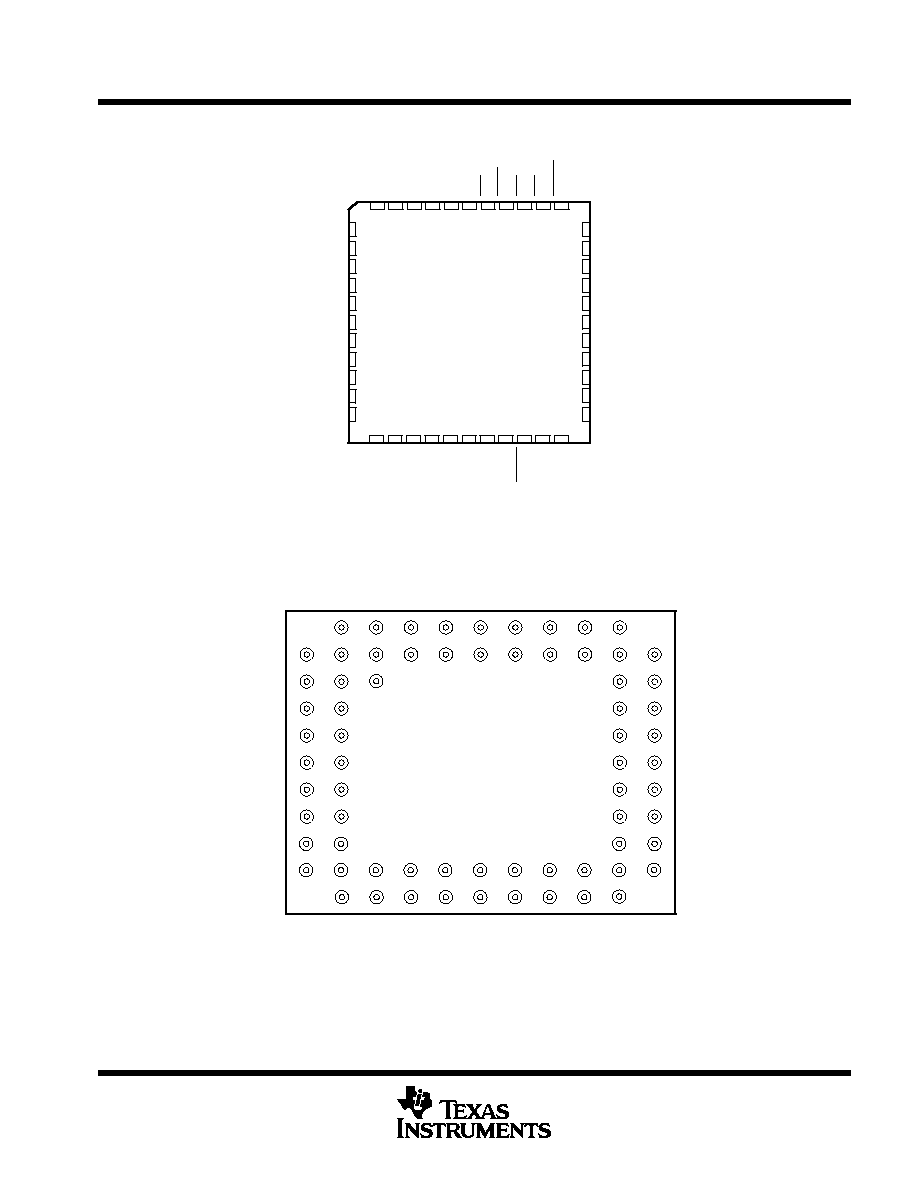
SN54ACT8990 . . . HV PACKAGE
(TOP VIEW)
CC
V
NC ≠ No internal connection
SN54ACT8990, SN74ACT8990
TEST-BUS CONTROLLERS
IEEE STD 1149.1 (JTAG) TAP MASTERS WITH 16-BIT GENERIC HOST INTERFACES
SCAS190E ≠ JUNE 1990 ≠ REVISED JANUARY 1997
3
POST OFFICE BOX 655303
∑
DALLAS, TEXAS 75265
RDY
RD
WR
TRST
ADRS4
ADRS3
ADRS2
ADRS1
ADRS0
GND
INT
DA
T
A15
T
OFF
TDI0
TDI1
DA
T
A
9
DA
T
A10
DA
T
A
1
1
DA
T
A12
DA
T
A13
DA
T
A14
CC
V
SN74ACT8990 . . . FN PACKAGE
(TOP VIEW)
TMS5/EVENT3
TMS4/EVENT2
TMS3/EVENT1
TMS2/EVENT0
V
CC
GND
TMS1
TMS0
TDO
TCKO
TCKI
39
38
37
36
35
34
33
32
31
30
29
18 19
7
8
9
10
11
12
13
14
15
16
17
DATA0
DATA1
DATA2
DATA3
DATA4
GND
V
CC
DATA5
DATA6
DATA7
DATA8
20 21 22 23
5
4
3
2
1
6
44
42 41 40
43
24 25 26 27 28
K
1
2
3
4
5
6
7
8
9
10
11
J
H
G
F
E
D
C
B
A
L
SN54ACT8990 . . . GB PACKAGE
(TOP VIEW)

SN54ACT8990, SN74ACT8990
TEST-BUS CONTROLLERS
IEEE STD 1149.1 (JTAG) TAP MASTERS WITH 16-BIT GENERIC HOST INTERFACES
SCAS190E ≠ JUNE 1990 ≠ REVISED JANUARY 1997
4
POST OFFICE BOX 655303
∑
DALLAS, TEXAS 75265
Table 1. Terminal Assignments
TERMINAL
TERMINAL
TERMINAL
TERMINAL
NO.
NAME
NO.
NAME
NO.
NAME
NO.
NAME
A2
NC
B10
NC
F11
NC
K6
NC
A3
ADRS4
B11
NC
G1
DATA5
K7
VCC
A4
NC
C1
DATA2
G2
NC
K8
DATA15
A5
ADRS1
C2
DATA1
G10
NC
K9
TDI0
A6
ADRS0
C3
NC
G11
TMS1
K10
NC
A7
NC
C10
TMS4/EVENT2
H1
NC
K11
TCKI
A8
INT
C11
TMS5/EVENT3
H2
DATA6
L2
DATA9
A9
RD
D1
DATA4
H10
TDO
L3
NC
A10
TRST
D2
DATA3
H11
TMS0
L4
DATA12
B1
DATA0
D10
TMS3/EVENT1
J1
DATA8
L5
DATA13
B2
NC
D11
NC
J2
DATA7
L6
NC
B3
ADRS3
E1
NC
J10
TCKO
L7
DATA14
B4
ADRS2
E2
GND
J11
NC
L8
TOFF
B5
NC
E10
VCC
K1
NC
L9
TDI1
B6
NC
E11
TMS2/EVENT0
K2
NC
L10
NC
B7
GND
F1
VCC
K3
DATA10
B8
RDY
F2
NC
K4
DATA11
B9
WR
F10
GND
K5
NC
NC ≠ No internal connection
functional block diagram
4
2
2
16
16
16
5
RD
WR
RDY
INT
ADRS(4 ≠ 0)
DATA(15 ≠ 0)
Host
Interface
Target
Interface
TMS(5 ≠ 2)/
EVENT(3 ≠ 0)
TMS(1 ≠ 0)
TDI(1 ≠ 0)
TDO
TOFF
TCKO
TCKI
TRST
Event
Block
Sequencer
Block
Counter Block
Command Block
Serial Block
Host
Block
Read Data Bus
Write Data Bus
Inputs have internal pullup resistors.

SN54ACT8990, SN74ACT8990
TEST-BUS CONTROLLERS
IEEE STD 1149.1 (JTAG) TAP MASTERS WITH 16-BIT GENERIC HOST INTERFACES
SCAS190E ≠ JUNE 1990 ≠ REVISED JANUARY 1997
5
POST OFFICE BOX 655303
∑
DALLAS, TEXAS 75265
Terminal Functions
TERMINAL NAME
I/O
DESCRIPTION
ADRS4 ≠ ADRS0
I
Address inputs. ADRS4 ≠ ADRS0 form the 5-bit address bus that interfaces the TBC to its host. These inputs
specify the TBC register to be read from or written to.
DATA15 ≠ DATA0
I/O
Data inputs and outputs. DATA15 ≠ DATA0 form the 16-bit bidirectional data bus that interfaces the TBC to its
host. Data is read from or written to the TBC register using this data bus.
GND
Ground
INT
O
Interrupt. INT transmits an interrupt signal to the host. When the TBC requires service from the host, INT is
asserted (low). INT will remain asserted (low) until the host has completed the required service.
NC
No connection
RD
I
Read strobe. RD is the active low output enable for the data bus. RD is used as the strobe for reading data from
the selected TBC register.
RDY
O
Ready. RDY transmits a status signal to the host. When the TBC is ready to accept a read or write operation
from the host, RDY is asserted (low). RDY is not asserted (high) when the TBC is in recovery from a read, write,
command, or reset operation.
TCKI
I
Test clock input. TCKI is the clock input for the TBC. Most operations of the TBC are synchronous to TCKI.
When enabled, all target interface outputs change on the falling edge of TCKI. Sampling of target interface
inputs are configured to occur on either the rising edge or falling edge of TCKI.
TCKO
O
Test clock output. TCKO distributes TCK to the target(s). The TCKO is configured to be disabled, constant zero,
constant one, or to follow TCKI. When TCKO follows TCKI, it is delayed to match the delay of generating the
TDO and TMS signals.
TDI1 ≠ TDI0
I
Test data inputs. The TDI1 ≠ TDI0 serial inputs are used for shifting test data from the target(s). The TDI inputs
can be directly connected to the TDO pin(s) of the target(s).
TDO
O
Test data output. TDO is used for shifting test data into the target(s). TDO can be directly connected to the TDI
terminal(s) of the target(s).
TMS1 ≠ TMS0
O
Test mode select outputs. These parallel outputs transmit TMS signals to the target(s), which direct them
through their TAP controller states. TMS1 ≠ TMS0 can be directly connected to the TMS terminals of the
target(s).
TMS5 ≠ TMS2/
EVENT3 ≠ EVENT0
I/O
Test mode select outputs or event inputs/outputs. These I/Os can be configured for use as either TMS outputs
or event inputs/outputs. As TMS outputs, they function similarly to TMS1 ≠ TMS0 above. As event I/Os, they
can be used to receive/transmit interrupt signals to/from the target(s).
TOFF
I
Test-off input. TOFF is the active low output disable for all outputs and I/Os of the target interface (TCKO, TDO,
TMS, TMS/EVENT).
TRST
I
Test-reset input. TRST is used to initiate hardware and software reset operations of the TBC. Hardware reset
begins when TRST is asserted (low). Software reset begins when TRST is released (high) and proceeds
synchronously to TCKI to completion in a predetermined number of cycles.
WR
I
Write input. WR is the strobe for writing data to a TBC data register. Signals present at the data and address
buses are captured on the rising edge of WR.
VCC
Supply voltage