SN54AHCT14, SN74AHCT14
HEX SCHMITT-TRIGGER INVERTERS
SCLS246P ≠ OCTOBER 1995 ≠ REVISED JULY 2003
1
POST OFFICE BOX 655303
∑
DALLAS, TEXAS 75265
D
Inputs Are TTL-Voltage Compatible
D
Latch-Up Performance Exceeds 250 mA Per
JESD 17
D
ESD Protection Exceeds JESD 22
≠ 2000-V Human-Body Model (A114-A)
≠ 200-V Machine Model (A115-A)
≠ 1000-V Charged-Device Model (C101)
1
2
3
4
5
6
7
14
13
12
11
10
9
8
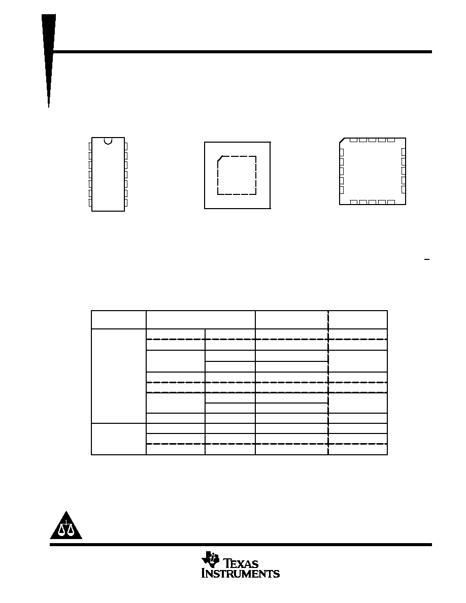
1A
1Y
2A
2Y
3A
3Y
GND
V
CC
6A
6Y
5A
5Y
4A
4Y
SN54AHCT14 . . . J OR W PACKAGE
SN74AHCT14 . . . D, DB, DGV, N, NS,
OR PW PACKAGE
(TOP VIEW)
3
2 1 20 19
9 10 11 12 13
4
5
6
7
8
18
17
16
15
14
6Y
NC
5A
NC
5Y
2A
NC
2Y
NC
3A
1Y
1A
NC
4Y
4A
V
6A
3Y
GND
NC
SN54AHCT14 . . . FK PACKAGE
(TOP VIEW)
CC
NC ≠ No internal connection
SN74AHCT14 . . . RGY PACKAGE
(TOP VIEW)
1
14
7
8
2
3
4
5
6
13
12
11
10
9
6A
6Y
5A
5Y
4A
1Y
2A
2Y
3A
3Y
1A
4Y
V
GND
CC
description/ordering information
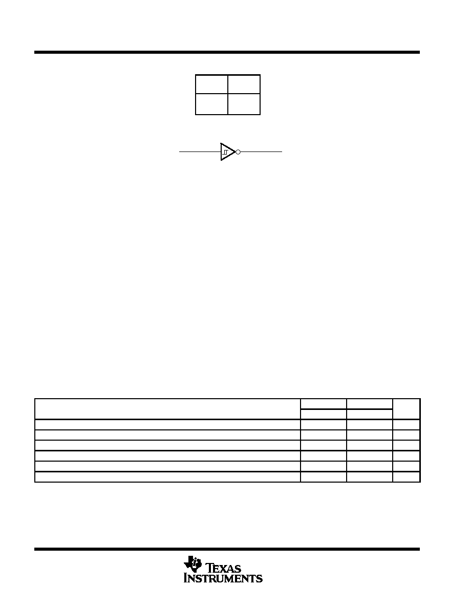
The 'AHCT14 devices contain six independent inverters. These devices perform the Boolean function Y = A.
Each circuit functions as an independent inverter, but because of the Schmitt action, the inverters have different
input threshold levels for positive-going (V
T+
) and for negative-going (V
T≠
) signals.
ORDERING INFORMATION
TA
PACKAGE
ORDERABLE
PART NUMBER
TOP-SIDE
MARKING
QFN ≠ RGY
Tape and reel
SN74AHCT14RGYR
HB14
PDIP ≠ N
Tube
SN74AHCT14N
SN74AHCT14N
SOIC ≠ D
Tube
SN74AHCT14D
AHCT14
SOIC ≠ D
Tape and reel
SN74AHCT14DR
AHCT14
≠40
∞
C to 85
∞
C
SOP ≠ NS
Tape and reel
SN74AHCT14NSR
AHCT14
SSOP ≠ DB
Tape and reel
SN74AHCT14DBR
HB14
TSSOP
PW
Tube
SN74AHCT14PW
HB14
TSSOP ≠ PW
Tape and reel
SN74AHCT14PWR
HB14
TVSOP ≠ DGV
Tape and reel
SN74AHCT14DGVR
HB14
CDIP ≠ J
Tube
SNJ54AHCT14J
SNJ54AHCT14J
≠55
∞
C to 125
∞
C
CFP ≠ W
Tube
SNJ54AHCT14W
SNJ54AHCT14W
LCCC ≠ FK
Tube
SNJ54AHCT14FK
SNJ54AHCT14FK
Package drawings, standard packing quantities, thermal data, symbolization, and PCB design guidelines
are available at www.ti.com/sc/package.
PRODUCTION DATA information is current as of publication date.
Products conform to specifications per the terms of Texas Instruments
standard warranty. Production processing does not necessarily include
testing of all parameters.
Copyright
2003, Texas Instruments Incorporated
Please be aware that an important notice concerning availability, standard warranty, and use in critical applications of
Texas Instruments semiconductor products and disclaimers thereto appears at the end of this data sheet.
On products compliant to MIL-PRF-38535, all parameters are tested
unless otherwise noted. On all other products, production
processing does not necessarily include testing of all parameters.
SN54AHCT14, SN74AHCT14
HEX SCHMITT-TRIGGER INVERTERS
SCLS246P ≠ OCTOBER 1995 ≠ REVISED JULY 2003
2
POST OFFICE BOX 655303
∑
DALLAS, TEXAS 75265
FUNCTION TABLE
(each inverter)
INPUT
A
OUTPUT
Y
H
L
L
H
logic diagram, each inverter (positive logic)
Y
A
absolute maximum ratings over operating free-air temperature range (unless otherwise noted)
Supply voltage range, V
CC
≠0.5 V to 7 V
. . . . . . . . . . . . . . . . . . . . . . . . . . . . . . . . . . . . . . . . . . . . . . . . . . . . . . . . . .
Input voltage range, V
I
(see Note 1)
≠0.5 V to 7 V
. . . . . . . . . . . . . . . . . . . . . . . . . . . . . . . . . . . . . . . . . . . . . . . . . .
Output voltage range, V
O
(see Note 1)
≠0.5 V to V
CC
+ 0.5 V
. . . . . . . . . . . . . . . . . . . . . . . . . . . . . . . . . . . . . . . .
Input clamp current, I
IK
(V
I
< 0)
≠20 mA
. . . . . . . . . . . . . . . . . . . . . . . . . . . . . . . . . . . . . . . . . . . . . . . . . . . . . . . . . . .
Output clamp current, I
OK
(V
O
< 0 or V
O
> V
CC
)
±
20 mA
. . . . . . . . . . . . . . . . . . . . . . . . . . . . . . . . . . . . . . . . . . . .
Continuous output current, I
O
(V
O
= 0 to V
CC
)
±
25 mA
. . . . . . . . . . . . . . . . . . . . . . . . . . . . . . . . . . . . . . . . . . . . . .
Continuous current through V
CC
or GND
±
50 mA
. . . . . . . . . . . . . . . . . . . . . . . . . . . . . . . . . . . . . . . . . . . . . . . . . . .
Package thermal impedance,
JA
(see Note 2): D package
86
∞
C/W
. . . . . . . . . . . . . . . . . . . . . . . . . . . . . . . . . . .
(see Note 2): DB package
96
∞
C/W
. . . . . . . . . . . . . . . . . . . . . . . . . . . . . . . . .
(see Note 2): DGV package
127
∞
C/W
. . . . . . . . . . . . . . . . . . . . . . . . . . . . . . .
(see Note 2): N package
80
∞
C/W
. . . . . . . . . . . . . . . . . . . . . . . . . . . . . . . . . . .
(see Note 2): NS package
76
∞
C/W
. . . . . . . . . . . . . . . . . . . . . . . . . . . . . . . . .
(see Note 2): PW package
113
∞
C/W
. . . . . . . . . . . . . . . . . . . . . . . . . . . . . . . .
(see Note 3): RGY package
47
∞
C/W
. . . . . . . . . . . . . . . . . . . . . . . . . . . . . . . .
Storage temperature range, T
stg
≠65
∞
C to 150
∞
C
. . . . . . . . . . . . . . . . . . . . . . . . . . . . . . . . . . . . . . . . . . . . . . . . . . .
Stresses beyond those listed under "absolute maximum ratings" may cause permanent damage to the device. These are stress ratings only, and
functional operation of the device at these or any other conditions beyond those indicated under "recommended operating conditions" is not
implied. Exposure to absolute-maximum-rated conditions for extended periods may affect device reliability.
NOTES:
1. The input and output voltage ratings may be exceeded if the input and output current ratings are observed.
2. The package thermal impedance is calculated in accordance with JESD 51-7.
3. The package thermal impedance is calculated in accordance with JESD 51-5.
recommended operating conditions (see Note 4)
SN54AHCT14
SN74AHCT14
UNIT
MIN
MAX
MIN
MAX
UNIT
VCC
Supply voltage
4.5
5.5
4.5
5.5
V
VI
Input voltage
0
5.5
0
5.5
V
VO
Output voltage
0
VCC
0
VCC
V
IOH
High-level output current
≠8
≠8
mA
IOL
Low-level output current
8
8
mA
TA
Operating free-air temperature
≠55
125
≠40
85
∞
C
NOTE 4: All unused inputs of the device must be held at VCC or GND to ensure proper device operation. Refer to the TI application report,
Implications of Slow or Floating CMOS Inputs, literature number SCBA004.
SN54AHCT14, SN74AHCT14
HEX SCHMITT-TRIGGER INVERTERS
SCLS246P ≠ OCTOBER 1995 ≠ REVISED JULY 2003
3
POST OFFICE BOX 655303
∑
DALLAS, TEXAS 75265
electrical characteristics over recommended operating free-air temperature range (unless
otherwise noted)
PARAMETER
TEST CONDITIONS
VCC
TA = 25
∞
C
SN54AHCT14
SN74AHCT14
UNIT
PARAMETER
TEST CONDITIONS
VCC
MIN
TYP
MAX
MIN
MAX
MIN
MAX
UNIT
VT+
Positive going input
4.5 V
0.9
1.9
0.9
1.9
0.9
1.9
V
Positive-going input
threshold voltage
5.5 V
1
2.1
1
2.1
1
2.1
V
VT≠
Negative going input
4.5 V
0.5
1.5
0.5
1.5
0.5
1.5
V
Negative-going input
threshold voltage
5.5 V
0.6
1.7
0.6
1.7
0.6
1.7
V
VT
Hysteresis
4.5 V
0.4
1.4
0.4
1.4
0.4
1.4
V
Hysteresis
(VT+ ≠ VT≠)
5.5 V
0.4
1.5
0.4
1.5
0.4
1.5
V
VOH
IOH = ≠50
m
A
4.5 V
4.4
4.5
4.4
4.4
V
VOH
IOH = ≠8 mA
4.5 V
3.94
3.8
3.8
V
VOL
IOL = 50
m
A
4.5 V
0.1
0.1
0.1
V
VOL
IOL = 8 mA
4.5 V
0.36
0.44
0.44
V
II
VI = 5.5 V or GND
0 V to 5.5 V
±
0.1
±
1*
±
1
m
A
ICC
VI = VCC or GND,
IO = 0
5.5 V
2
20
20
m
A
ICC
One input at 3.4 V,
Other inputs at VCC or GND
5.5 V
1.35
1.5
1.5
mA
Ci
VI = VCC or GND
5 V
2
10
10
pF
* On products compliant to MIL-PRF-38535, this parameter is not production tested at VCC = 0 V.
This is the increase in supply current for each input at one of the specified TTL voltage levels, rather than 0 V or VCC.
switching characteristics over recommended operating free-air temperature range
V
CC
= 5 V
±
0.5 V (unless otherwise noted) (see Figure 1)
PARAMETER
FROM
TO
LOAD
TA = 25
∞
C
SN54AHCT14
SN74AHCT14
UNIT
PARAMETER
(INPUT)
(OUTPUT)
CAPACITANCE
MIN
TYP
MAX
MIN
MAX
MIN
MAX
UNIT
tPLH
A
Y
CL = 15 pF
4**
7**
1**
8**
1
8
ns
tPHL
A
Y
CL = 15 pF
4**
7**
1**
8**
1
8
ns
tPLH
A
Y
CL = 50 pF
5.5
8
1
9
1
9
ns
tPHL
A
Y
CL = 50 pF
5.5
8
1
9
1
9
ns
** On products compliant to MIL-PRF-38535, this parameter is not production tested.
noise characteristics, V
CC
= 5 V, C
L
= 50 pF, T
A
= 25
∞
C (see Note 5)
PARAMETER
SN74AHCT14
UNIT
PARAMETER
MIN
TYP
MAX
UNIT
VOL(P)
Quiet output, maximum dynamic VOL
0.9
V
VOL(V)
Quiet output, minimum dynamic VOL
≠0.7
V
VOH(V)
Quiet output, minimum dynamic VOH
4.3
V
VIH(D)
High-level dynamic input voltage
2.1
V
VIL(D)
Low-level dynamic input voltage
0.5
V
NOTE 5: Characteristics are for surface-mount packages only.
operating characteristics, V
CC
= 5 V, T
A
= 25
∞
C
PARAMETER
TEST CONDITIONS
TYP
UNIT
Cpd
Power dissipation capacitance
No load,
f = 1 MHz
12
pF
SN54AHCT14, SN74AHCT14
HEX SCHMITT-TRIGGER INVERTERS
SCLS246P ≠ OCTOBER 1995 ≠ REVISED JULY 2003
4
POST OFFICE BOX 655303
∑
DALLAS, TEXAS 75265
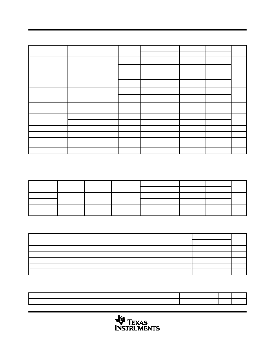
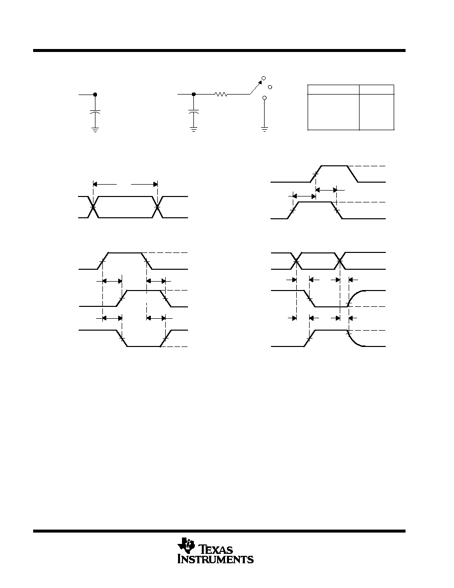
PARAMETER MEASUREMENT INFORMATION
50% VCC
3 V
3 V
0 V
0 V
th
tsu
VOLTAGE WAVEFORMS
SETUP AND HOLD TIMES
Data Input
tPLH
tPHL
tPHL
tPLH
VOH
VOH
VOL
VOL
3 V
0 V
50% VCC
50% VCC
Input
Out-of-Phase
Output
In-Phase
Output
Timing Input
50% VCC
VOLTAGE WAVEFORMS
PROPAGATION DELAY TIMES
INVERTING AND NONINVERTING OUTPUTS
Output
Control
Output
Waveform 1
S1 at VCC
(see Note B)
Output
Waveform 2
S1 at GND
(see Note B)
VOL
VOH
tPZL
tPZH
tPLZ
tPHZ
VCC
0 V
50% VCC
VOL
+ 0.3 V
50% VCC
0 V
3 V
VOLTAGE WAVEFORMS
ENABLE AND DISABLE TIMES
LOW- AND HIGH-LEVEL ENABLING
tPLH/tPHL
tPLZ/tPZL
tPHZ/tPZH
Open Drain
Open
VCC
GND
VCC
TEST
S1
3 V
0 V
tw
VOLTAGE WAVEFORMS
PULSE DURATION
Input
NOTES: A. CL includes probe and jig capacitance.
B. Waveform 1 is for an output with internal conditions such that the output is low except when disabled by the output control.
Waveform 2 is for an output with internal conditions such that the output is high except when disabled by the output control.
C. All input pulses are supplied by generators having the following characteristics: PRR
1 MHz, ZO = 50
, tr
3 ns, tf
3 ns.
D. The outputs are measured one at a time with one input transition per measurement.
E. All parameters and waveforms are not applicable to all devices.
From Output
Under Test
CL
(see Note A)
LOAD CIRCUIT FOR
3-STATE AND OPEN-DRAIN OUTPUTS
S1
VCC
RL = 1 k
GND
From Output
Under Test
CL
(see Note A)
Test
Point
LOAD CIRCUIT FOR
TOTEM-POLE OUTPUTS
Open
VOH ≠
0.3 V
1.5 V
1.5 V
1.5 V
1.5 V
1.5 V
1.5 V
1.5 V
1.5 V
1.5 V
Figure 1. Load Circuit and Voltage Waveforms