SN54ALVTH16244, SN74ALVTH16244
2.5-V/3.3-V 16-BIT BUFFERS/DRIVERS
WITH 3-STATE OUTPUTS
SCES070G ≠ JUNE 1996 ≠ REVISED MAY 1999
1
POST OFFICE BOX 655303
∑
DALLAS, TEXAS 75265
D
Members of the Texas Instruments
Widebus
TM
Family
D
State-of-the-Art Advanced BiCMOS
Technology (ABT) Design for 3.3-V
Operation and Low Static-Power
Dissipation
D
5-V I/O Compatible
D
High Drive Capability (≠32 mA/64 mA)
D
Support Mixed-Mode Signal Operation (5-V
Input and Output Voltages With 3.3-V V
CC
)
D
Support Unregulated Battery Operation
Down to 2.3 V
D
Typical V
OLP
(Output Ground Bounce)
< 0.8 V at V
CC
= 3.3 V, T
A
= 25
∞
C
D
Auto3-State Eliminates Bus Current
Loading When Voltage at the Output
Exceeds V
CC
D
I
off
and Power-Up 3-State Support Hot
Insertion
D
Bus Hold on Data Inputs Eliminates the
Need for External Pullup/Pulldown
Resistors
D
Latch-Up Performance Exceeds 250 mA Per
JESD 17
D
ESD Protection Exceeds 2000 V Per
MIL-STD-883, Method 3015; Exceeds 200 V
Using Machine Model (C = 200 pF, R = 0)
D
Package Options Include Plastic 300-mil
Shrink Small-Outline (DL), Thin Shrink
Small-Outline (DGG), Thin Very
Small-Outline (DGV) Packages, and 380-mil
Fine-Pitch Ceramic Flat (WD) Package
NOTE: For tape and reel order entry:
The DGGR package is abbreviated to GR, and
the DGVR package is abbreviated to VR.
description
The 'ALVTH16244 devices are 16-bit buffers/line drivers designed for 2.5-V or 3.3-V V
CC
operation, but with
the capability to provide a TTL interface to a 5-V system environment. These devices can be used as four 4-bit
buffers, two 8-bit buffers, or one 16-bit buffer.
Active bus-hold circuitry is provided to hold unused or floating data inputs at a valid logic level.
Copyright
©
1999, Texas Instruments Incorporated
UNLESS OTHERWISE NOTED this document contains PRODUCTION
DATA information current as of publication date. Products conform to
specifications per the terms of Texas Instruments standard warranty.
Production processing does not necessarily include testing of all
parameters.
Please be aware that an important notice concerning availability, standard warranty, and use in critical applications of
Texas Instruments semiconductor products and disclaimers thereto appears at the end of this data sheet.
Widebus is a trademark of Texas Instruments Incorporated.
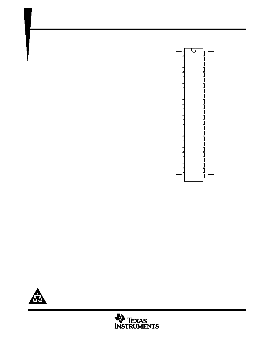
SN54ALVTH16244 . . . WD PACKAGE
SN74ALVTH16244 . . . DGG, DGV, OR DL PACKAGE
(TOP VIEW)
1
2
3
4
5
6
7
8
9
10
11
12
13
14
15
16
17
18
19
20
21
22
23
24
48
47
46
45
44
43
42
41
40
39
38
37
36
35
34
33
32
31
30
29
28
27
26
25
1OE
1Y1
1Y2
GND
1Y3
1Y4
V
CC
2Y1
2Y2
GND
2Y3
2Y4
3Y1
3Y2
GND
3Y3
3Y4
V
CC
4Y1
4Y2
GND
4Y3
4Y4
4OE
2OE
1A1
1A2
GND
1A3
1A4
V
CC
2A1
2A2
GND
2A3
2A4
3A1
3A2
GND
3A3
3A4
V
CC
4A1
4A2
GND
4A3
4A4
3OE

SN54ALVTH16244, SN74ALVTH16244
2.5-V/3.3-V 16-BIT BUFFERS/DRIVERS
WITH 3-STATE OUTPUTS
SCES070G ≠ JUNE 1996 ≠ REVISED MAY 1999
2
POST OFFICE BOX 655303
∑
DALLAS, TEXAS 75265
description (continued)
When V
CC
is between 0 and 1.2 V, the device is in the high-impedance state during power up or power down.
However, to ensure the high-impedance state above 1.2 V, the output-enable (OE) input should be tied to V
CC
through a pullup resistor; the minimum value of the resistor is determined by the current-sinking capability of
the driver.
These devices are fully specified for hot-insertion applications using I
off
and power-up 3-state. The I
off
circuitry
disables the outputs, preventing damaging current backflow through the devices when they are powered down.
The power-up 3-state circuitry places the outputs in the high-impedance state during power up and power down,
which prevents driver conflict.
The SN54ALVTH16244 is characterized for operation over the full military temperature range of ≠55
∞
C to
125
∞
C. The SN74ALVTH16244 is characterized for operation from ≠40
∞
C to 85
∞
C.
FUNCTION TABLE
(each buffer)
INPUTS
OUTPUT
OE
A
Y
L
H
H
L
L
L
H
X
Z
logic diagram (positive logic)
1OE
1A1
1A2
1A3
1A4
1Y1
1Y2
1Y3
1Y4
1
47
46
44
43
2
3
5
6
2OE
2A1
2A2
2A3
2A4
2Y1
2Y2
2Y3
2Y4
48
41
40
38
37
8
9
11
12
3OE
3A1
3A2
3A3
3A4
3Y1
3Y2
3Y3
3Y4
25
36
35
33
32
13
14
16
17
4OE
4A1
4A2
4A3
4A4
4Y1
4Y2
4Y3
4Y4
24
30
29
27
26
19
20
22
23
SN54ALVTH16244, SN74ALVTH16244
2.5-V/3.3-V 16-BIT BUFFERS/DRIVERS
WITH 3-STATE OUTPUTS
SCES070G ≠ JUNE 1996 ≠ REVISED MAY 1999
3
POST OFFICE BOX 655303
∑
DALLAS, TEXAS 75265
absolute maximum ratings over operating free-air temperature range (unless otherwise noted)
Supply voltage range, V
CC
≠0.5 V to 4.6 V
. . . . . . . . . . . . . . . . . . . . . . . . . . . . . . . . . . . . . . . . . . . . . . . . . . . . . . . . .
Input voltage range, V
I
(see Note 1)
≠0.5 V to 7 V
. . . . . . . . . . . . . . . . . . . . . . . . . . . . . . . . . . . . . . . . . . . . . . . . . .
Voltage range applied to any output in
the high-impedance
or power-off state, V
O
(see Note 1)
≠0.5 V to 7 V
. . . . . . . . . . . . . . . . . . . . . . . . . . . . . . . . . . . . . . . . . . . . . . . .
Voltage range applied to any output in the high state, V
O
(see Note 1)
≠0.5 V to V
CC
to 7V
. . . . . . . . . . . . . .
Output current in the low state, I
O
: SN54ALVTH16244 96
mA
. . . . . . . . . . . . . . . . . . . . . . . . . . . . . . . . . . . . . . . .
SN74ALVTH16244 128
mA
. . . . . . . . . . . . . . . . . . . . . . . . . . . . . . . . . . . . . . .
Output current in the high state, I
O
: SN54ALVTH16244 ≠48
mA
. . . . . . . . . . . . . . . . . . . . . . . . . . . . . . . . . . . . . .
SN74ALVTH16244 ≠64
mA
. . . . . . . . . . . . . . . . . . . . . . . . . . . . . . . . . . . . . .
Input clamp current, I
IK
(V
I
< 0)
≠50 mA
. . . . . . . . . . . . . . . . . . . . . . . . . . . . . . . . . . . . . . . . . . . . . . . . . . . . . . . . . . .
Output clamp current, I
OK
(V
O
< 0)
≠50 mA
. . . . . . . . . . . . . . . . . . . . . . . . . . . . . . . . . . . . . . . . . . . . . . . . . . . . . . . .
Package thermal impedance,
JA
(see Note 2): DGG package
89
∞
C/W
. . . . . . . . . . . . . . . . . . . . . . . . . . . . . . .
DGV package
93
∞
C/W
. . . . . . . . . . . . . . . . . . . . . . . . . . . . . . . .
DL package
94
∞
C/W
. . . . . . . . . . . . . . . . . . . . . . . . . . . . . . . . .
Storage temperature range, T
stg
≠65
∞
C to 150
∞
C
. . . . . . . . . . . . . . . . . . . . . . . . . . . . . . . . . . . . . . . . . . . . . . . . . . .
Stresses beyond those listed under "absolute maximum ratings" may cause permanent damage to the device. These are stress ratings only, and
functional operation of the device at these or any other conditions beyond those indicated under "recommended operating conditions" is not
implied. Exposure to absolute-maximum-rated conditions for extended periods may affect device reliability.
NOTES:
1. The input and output negative-voltage ratings may be exceeded if the input and output clamp-current ratings are observed.
2. The package thermal impedance is calculated in accordance with JESD 51.
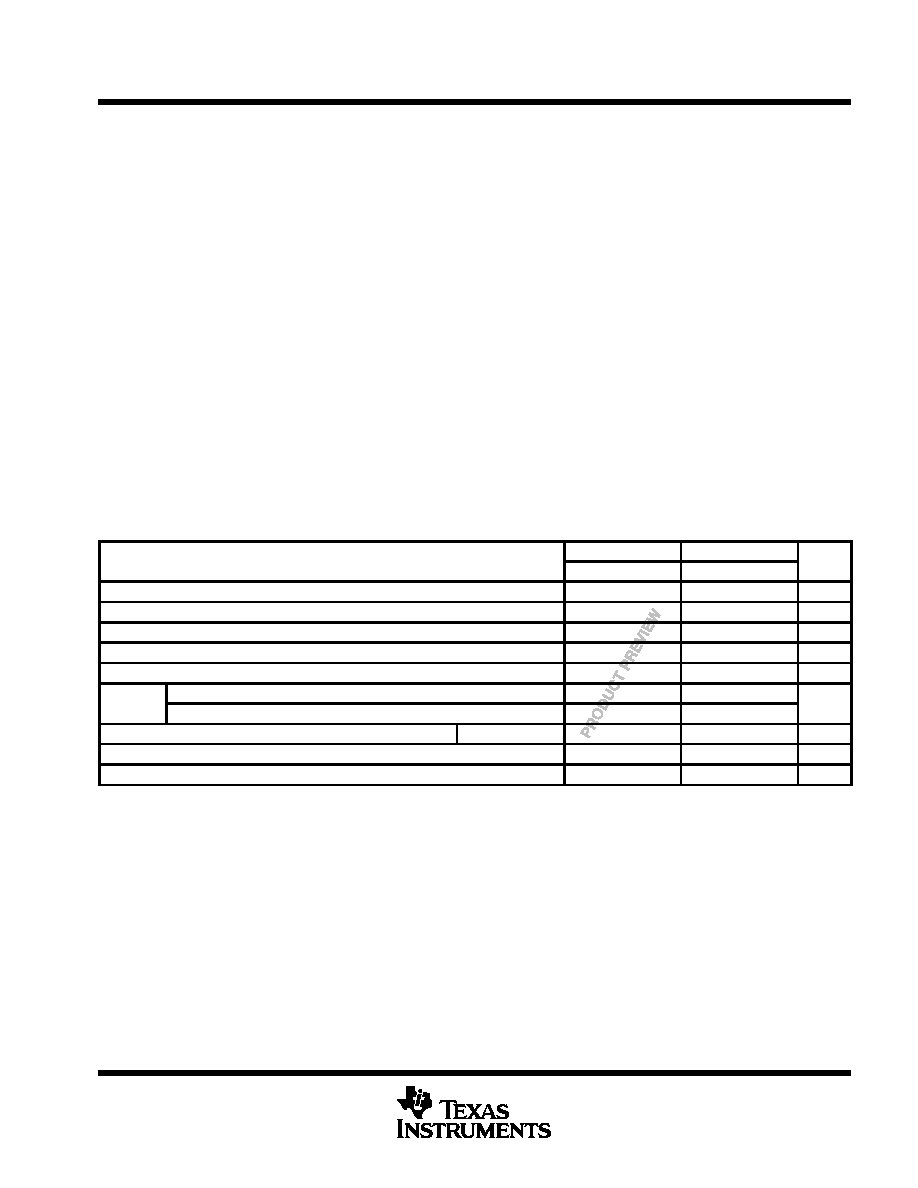
recommended operating conditions, V
CC
= 2.5 V
±
0.2 V (see Note 3)
SN54ALVTH16244
SN74ALVTH16244
UNIT
MIN
MAX
MIN
MAX
UNIT
VCC
Supply voltage
2.3
2.7
2.3
2.7
V
VIH
High-level input voltage
1.7
1.7
V
VIL
Low-level input voltage
0.7
0.7
V
VI
Input voltage
0
5.5
0
5.5
V
IOH
High-level output current
≠6
≠8
mA
IOL
Low-level output current
6
8
mA
IOL
Low-level output current; current duty cycle
50%; f
1 kHz
18
24
mA
t/
v
Input transition rise or fall rate
Outputs enabled
10
10
ns/V
t/
VCC
Power-up ramp rate
200
200
µ
s/V
TA
Operating free-air temperature
≠55
125
≠40
85
∞
C
NOTE 3: All unused control inputs of the device must be held at VCC or GND to ensure proper device operation. Refer to the TI application report,
Implications of Slow or Floating CMOS Inputs, literature number SCBA004.
PRODUCT PREVIEW information concerns products in the formative or
design phase of development. Characteristic data and other
specifications are design goals. Texas Instruments reserves the right to
change or discontinue these products without notice.
SN54ALVTH16244, SN74ALVTH16244
2.5-V/3.3-V 16-BIT BUFFERS/DRIVERS
WITH 3-STATE OUTPUTS
SCES070G ≠ JUNE 1996 ≠ REVISED MAY 1999
4
POST OFFICE BOX 655303
∑
DALLAS, TEXAS 75265
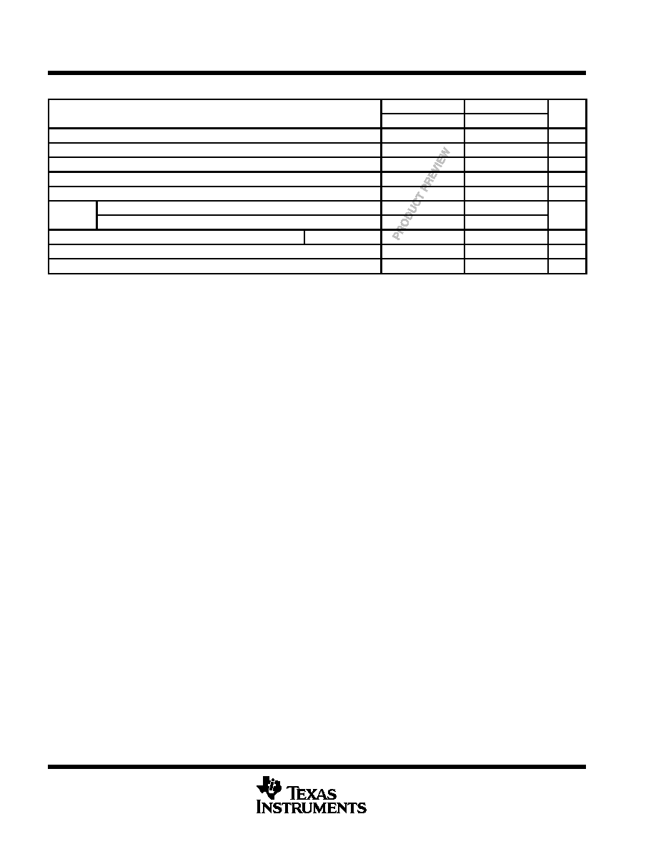
recommended operating conditions, V
CC
= 3.3 V
±
0.3 V (see Note 3)
SN54ALVTH16244
SN74ALVTH16244
UNIT
MIN
MAX
MIN
MAX
UNIT
VCC
Supply voltage
3
3.6
3
3.6
V
VIH
High-level input voltage
2
2
V
VIL
Low-level input voltage
0.8
0.8
V
VI
Input voltage
0
5.5
0
5.5
V
IOH
High-level output current
≠24
≠32
mA
IOL
Low-level output current
24
32
mA
IOL
Low-level output current; current duty cycle
50%; f
1 kHz
48
64
mA
t/
v
Input transition rise or fall rate
Outputs enabled
10
10
ns/V
t/
VCC
Power-up ramp rate
200
200
µ
s/V
TA
Operating free-air temperature
≠55
125
≠40
85
∞
C
NOTE 3: All unused control inputs of the device must be held at VCC or GND to ensure proper device operation. Refer to the TI application report,
Implications of Slow or Floating CMOS Inputs, literature number SCBA004.
PRODUCT PREVIEW information concerns products in the formative or
design phase of development. Characteristic data and other
specifications are design goals. Texas Instruments reserves the right to
change or discontinue these products without notice.
SN54ALVTH16244, SN74ALVTH16244
2.5-V/3.3-V 16-BIT BUFFERS/DRIVERS
WITH 3-STATE OUTPUTS
SCES070G ≠ JUNE 1996 ≠ REVISED MAY 1999
5
POST OFFICE BOX 655303
∑
DALLAS, TEXAS 75265
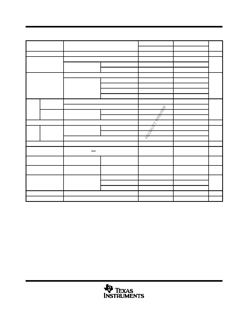
electrical characteristics over recommended operating free-air temperature range,
V
CC
= 2.5 V
±
0.2 V (unless otherwise noted)
PARAMETER
TEST CONDITIONS
SN54ALVTH16244
SN74ALVTH16244
UNIT
PARAMETER
TEST CONDITIONS
MIN
TYP
MAX
MIN
TYP
MAX
UNIT
VIK
VCC = 2.3 V,
II = ≠18 mA
≠1.2
≠1.2
V
VCC = 2.3 V to 2.7 V,
IOH = ≠100
µ
A
VCC≠0.2
VCC≠0.2
VOH
VCC = 2 3 V
IOH = ≠6 mA
1.8
V
VCC = 2.3 V
IOH = ≠8 mA
1.8
VCC = 2.3 V to 2.7 V,
IOL = 100
µ
A
0.2
0.2
IOL = 6 mA
0.4
VOL
VCC = 2 3 V
IOL = 8 mA
0.4
V
VCC = 2.3 V
IOL = 18 mA
0.5
IOL = 24 mA
0.5
Control inputs
VCC = 2.7 V,
VI = VCC or GND
±
1
±
1
II
Control inputs
VCC = 0 or 2.7 V,
VI = 5.5 V
10
10
µ
A
II
Data inputs
VCC = 2 7 V
VI = VCC
1
1
µ
A
Data inputs
VCC = 2.7 V
VI = 0
≠5
≠5
Ioff
VCC = 0,
VI or VO = 0 to 4.5 V
±
100
µ
A
VCC = 2 3 V
VI = 0.7 V
115
115
II(hold) Data inputs
VCC = 2.3 V
VI = 1.7 V
≠10
≠10
µ
A
I(hold)
VCC = 2.7 V,
VI = 0 to 2.7 V
±
300
±
300
IEXß
VCC = 2.3 V,
VO = 5.5 V
125
125
µ
A
IOZ(PU/PD)∂
VCC
1.2 V, VO = 0.5 V to VCC,
VI = GND or VCC, OE = don't care
±
100
±
100
µ
A
IOZH
VCC = 2.7 V
VO = 2.3 V,
VI = 0.7 V or 1.7 V
5
5
µ
A
IOZL
VCC = 2.7 V
VO = 0.5 V,
VI = 0.7 V or 1.7 V
≠5
≠5
µ
A
VCC = 2.7 V,
Outputs high
0.04
0.1
0.04
0.1
ICC
VCC = 2.7 V,
IO = 0,
Outputs low
2.3
4.5
2.3
4.5
mA
VI = VCC or GND
Outputs disabled
0.04
0.1
0.04
0.1
Ci
VCC = 2.5 V,
VI = 2.5 V or 0
3
3
pF
Co
VCC = 2.5 V,
VO = 2.5 V or 0
6
6
pF
All typical values are at VCC = 2.5 V, TA = 25
∞
C.
This is the bus-hold maximum dynamic current. It is the minimum overdrive current required to switch the input from one state to another.
ß Current into an output in the high state when VO > VCC
∂ High-impedance state during power up/power down
PRODUCT PREVIEW information concerns products in the formative or
design phase of development. Characteristic data and other
specifications are design goals. Texas Instruments reserves the right to
change or discontinue these products without notice.
SN54ALVTH16244, SN74ALVTH16244
2.5-V/3.3-V 16-BIT BUFFERS/DRIVERS
WITH 3-STATE OUTPUTS
SCES070G ≠ JUNE 1996 ≠ REVISED MAY 1999
6
POST OFFICE BOX 655303
∑
DALLAS, TEXAS 75265
electrical characteristics over recommended operating free-air temperature range,
V
CC
= 3.3 V
±
0.3 V (unless otherwise noted)
PARAMETER
TEST CONDITIONS
SN54ALVTH16244
SN74ALVTH16244
UNIT
PARAMETER
TEST CONDITIONS
MIN
TYP
MAX
MIN
TYP
MAX
UNIT
VIK
VCC = 3 V,
II = ≠18 mA
≠1.2
≠1.2
V
VCC = 3 V to 3.6 V,
IOH = ≠100
µ
A
VCC≠0.2
VCC≠0.2
VOH
VCC = 3 V
IOH = ≠24 mA
2
V
VCC = 3 V
IOH = ≠32 mA
2
VCC = 3 V to 3.6 V,
IOL = 100
µ
A
0.2
0.2
IOL = 16 mA
0.4
VOL
IOL = 24 mA
0.5
V
VOL
VCC = 3 V
IOL = 32 mA
0.5
V
IOL = 48 mA
0.55
IOL = 64 mA
0.55
Control inputs
VCC = 3.6 V,
VI = VCC or GND
±
1
±
1
Control inputs
VCC = 0 or 3.6 V,
VI = 5.5 V
10
10
II
VI = 5.5 V
20
20
µ
A
Data inputs
VCC = 3.6 V
VI = VCC
1
1
VI = 0
≠5
≠5
Ioff
VCC = 0,
VI or VO = 0 to 4.5 V
±
100
µ
A
VCC = 3 V
VI = 0.8 V
75
75
II(hold) Data inputs
VCC = 3 V
VI = 2 V
≠75
≠75
µ
A
I(hold)
VCC = 3.6 V,
VI = 0 to 3.6 V
±
500
±
500
IEXß
VCC = 3 V,
VO = 5.5 V
125
125
µ
A
IOZ(PU/PD)∂
VCC
1.2 V, VO = 0.5 V to VCC,
VI = GND or VCC, OE = don't care
±
100
±
100
µ
A
IOZH
VCC = 3.6 V
VO = 3 V,
VI = 0.8 V or 2 V
5
5
µ
A
IOZL
VCC = 3.6 V
VO = 0.5 V,
VI = 0.8 V or 2 V
≠5
≠5
µ
A
VCC = 3.6 V,
Outputs high
0.07
0.1
0.07
0.1
ICC
VCC = 3.6 V,
IO = 0,
Outputs low
3.2
5
3.2
5
mA
VI = VCC or GND
Outputs disabled
0.07
0.1
0.07
0.1
ICC#
VCC = 3 V to 3.6 V, One input at VCC ≠ 0.6 V,
Other inputs at VCC or GND
0.4
0.4
mA
Ci
VCC = 3.3 V,
VI = 3.3 V or 0
3
3
pF
Co
VCC = 3.3 V,
VO = 3.3 V or 0
6
6
pF
All typical values are at VCC = 3.3 V, TA = 25
∞
C.
This is the bus-hold maximum dynamic current. It is the minimum overdrive current required to switch the input from one state to another.
ß Current into an output in the high state when VO > VCC
∂ High-impedance state during power up/power down
# This is the increase in supply current for each input that is at the specified TTL voltage level rather than VCC or GND.
PRODUCT PREVIEW information concerns products in the formative or
design phase of development. Characteristic data and other
specifications are design goals. Texas Instruments reserves the right to
change or discontinue these products without notice.
SN54ALVTH16244, SN74ALVTH16244
2.5-V/3.3-V 16-BIT BUFFERS/DRIVERS
WITH 3-STATE OUTPUTS
SCES070G ≠ JUNE 1996 ≠ REVISED MAY 1999
7
POST OFFICE BOX 655303
∑
DALLAS, TEXAS 75265
switching characteristics over recommended operating free-air temperature range, C
L
= 30 pF,
V
CC
= 2.5 V
±
0.2 V (unless otherwise noted) (see Figure 1)
PARAMETER
FROM
TO
SN54ALVTH16244
SN74ALVTH16244
UNIT
PARAMETER
(INPUT)
(OUTPUT)
MIN
MAX
MIN
MAX
UNIT
tPLH
A
Y
1
3.1
1
3
ns
tPHL
A
Y
1
3.6
1
3.5
ns
tPZH
OE
Y
1.1
6
1.1
5.9
ns
tPZL
OE
Y
1.1
4.8
1.1
4.7
ns
tPHZ
OE
Y
1.5
4.5
1.5
4.4
ns
tPLZ
OE
Y
1
3.5
1
3.4
ns
switching characteristics over recommended operating free-air temperature range, C
L
= 50 pF,
V
CC
= 3.3 V
±
0.3 V (unless otherwise noted) (see Figure 2)
PARAMETER
FROM
TO
SN54ALVTH16244
SN74ALVTH16244
UNIT
PARAMETER
(INPUT)
(OUTPUT)
MIN
MAX
MIN
MAX
UNIT
tPLH
A
Y
1
2.6
1
2.4
ns
tPHL
A
Y
1
2.6
1
2.5
ns
tPZH
OE
Y
1
3.9
1
3.8
ns
tPZL
OE
Y
1
3
1
2.9
ns
tPHZ
OE
Y
1.5
4.3
1.5
4.2
ns
tPLZ
OE
Y
1.5
3.7
1.5
3.6
ns
PRODUCT PREVIEW information concerns products in the formative or
design phase of development. Characteristic data and other
specifications are design goals. Texas Instruments reserves the right to
change or discontinue these products without notice.
SN54ALVTH16244, SN74ALVTH16244
2.5-V/3.3-V 16-BIT BUFFERS/DRIVERS
WITH 3-STATE OUTPUTS
SCES070G ≠ JUNE 1996 ≠ REVISED MAY 1999
8
POST OFFICE BOX 655303
∑
DALLAS, TEXAS 75265
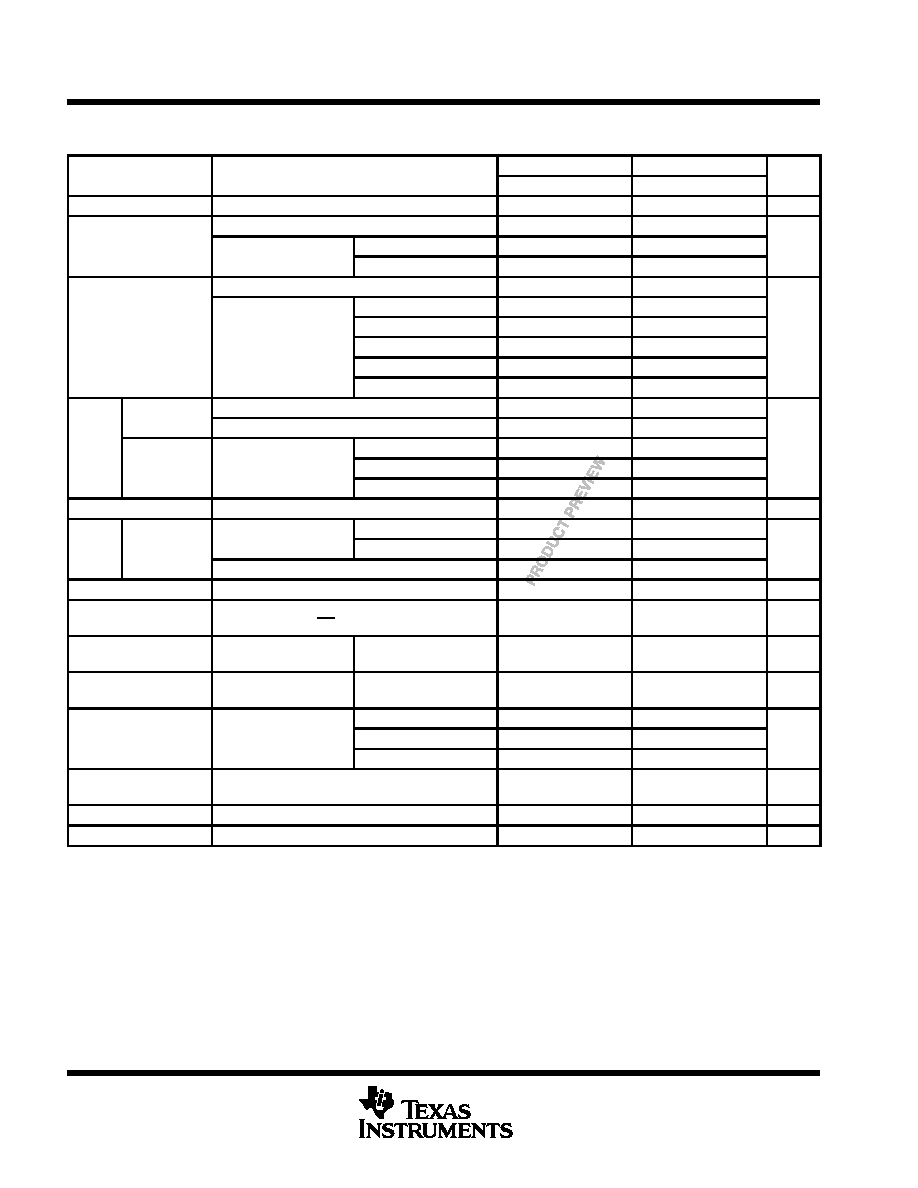
PARAMETER MEASUREMENT INFORMATION
V
CC
= 2.5 V
±
0.2 V
VCC/2
VCC/2
VCC/2
VCC/2
VCC/2
VCC/2
VCC/2
VCC/2
VOH
VOL
th
tsu
From Output
Under Test
CL = 30 pF
(see Note A)
LOAD CIRCUIT
S1
Open
GND
500
500
Output
Control
(low-level
enabling)
Output
Waveform 1
S1 at 2
◊
VCC
(see Note B)
Output
Waveform 2
S1 at GND
(see Note B)
tPZL
tPZH
tPLZ
tPHZ
0 V
VOL + 0.15 V
VOH ≠ 0.15 V
0 V
VCC
0 V
0 V
tw
VCC
VCC
VOLTAGE WAVEFORMS
SETUP AND HOLD TIMES
VOLTAGE WAVEFORMS
PULSE DURATION
VOLTAGE WAVEFORMS
ENABLE AND DISABLE TIMES
Timing
Input
Data
Input
Input
tPLH/tPHL
tPLZ/tPZL
tPHZ/tPZH
Open
2
◊
VCC
GND
TEST
S1
NOTES: A. CL includes probe and jig capacitance.
B. Waveform 1 is for an output with internal conditions such that the output is low except when disabled by the output control.
Waveform 2 is for an output with internal conditions such that the output is high except when disabled by the output control.
C. All input pulses are supplied by generators having the following characteristics: PRR
10 MHz, ZO = 50
, tr
2 ns, tf
2 ns.
D. The outputs are measured one at a time with one transition per measurement.
0 V
VCC
VCC/2
tPHL
VCC/2
VCC/2
VCC
0 V
VOH
VOL
Input
Output
VOLTAGE WAVEFORMS
PROPAGATION DELAY TIMES
VCC/2
VCC/2
tPLH
2
◊
VCC
VCC
Figure 1. Load Circuit and Voltage Waveforms
SN54ALVTH16244, SN74ALVTH16244
2.5-V/3.3-V 16-BIT BUFFERS/DRIVERS
WITH 3-STATE OUTPUTS
SCES070G ≠ JUNE 1996 ≠ REVISED MAY 1999
9
POST OFFICE BOX 655303
∑
DALLAS, TEXAS 75265
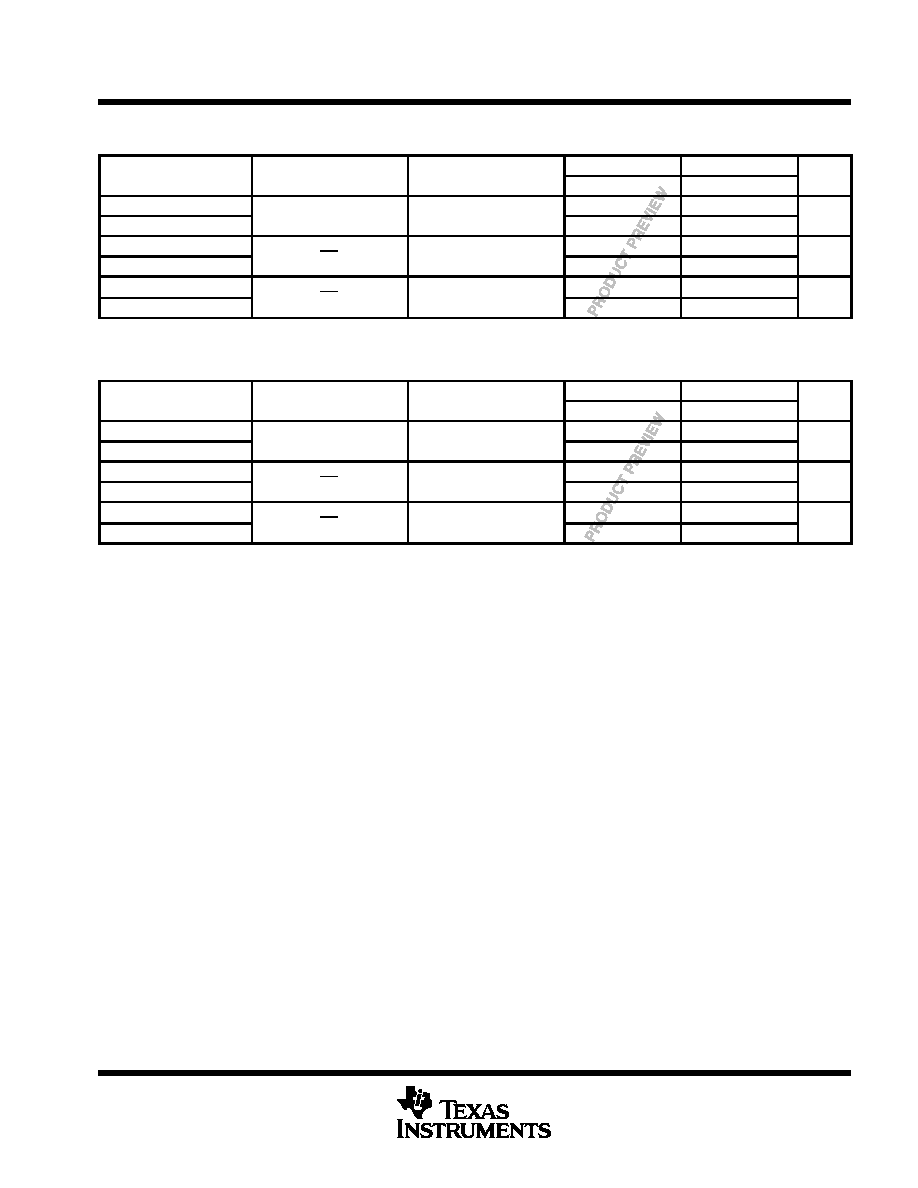
PARAMETER MEASUREMENT INFORMATION
V
CC
= 3.3 V
±
0.3 V
VOH
VOL
th
tsu
From Output
Under Test
CL = 50 pF
(see Note A)
LOAD CIRCUIT
S1
Open
GND
500
500
tPLH
tPHL
Output Control
Output
Waveform 1
S1 at 6 V
(see Note B)
Output
Waveform 2
S1 at GND
(see Note B)
tPZL
tPZH
tPLZ
tPHZ
3 V
0 V
VOH
VOL
0 V
VOL + 0.3 V
VOH ≠ 0.3 V
0 V
3 V
0 V
0 V
tw
Input
3 V
3 V
3 V
VOLTAGE WAVEFORMS
SETUP AND HOLD TIMES
VOLTAGE WAVEFORMS
PROPAGATION DELAY TIMES
INVERTING AND NONINVERTING OUTPUTS
VOLTAGE WAVEFORMS
PULSE DURATION
VOLTAGE WAVEFORMS
ENABLE AND DISABLE TIMES
LOW- AND HIGH-LEVEL ENABLING
Timing
Input
Data
Input
Output
Input
tPLH/tPHL
tPLZ/tPZL
tPHZ/tPZH
Open
6 V
GND
TEST
S1
NOTES: A. CL includes probe and jig capacitance.
B. Waveform 1 is for an output with internal conditions such that the output is low except when disabled by the output control.
Waveform 2 is for an output with internal conditions such that the output is high except when disabled by the output control.
C. All input pulses are supplied by generators having the following characteristics: PRR
10 MHz, ZO = 50
, tr
2.5 ns, tf
2.5 ns.
D. The outputs are measured one at a time with one transition per measurement.
6 V
1.5 V
1.5 V
1.5 V
1.5 V
1.5 V
0 V
3 V
1.5 V
1.5 V
1.5 V
1.5 V
1.5 V
1.5 V
1.5 V
1.5 V
Figure 2. Load Circuit and Voltage Waveforms

IMPORTANT NOTICE
Texas Instruments and its subsidiaries (TI) reserve the right to make changes to their products or to discontinue
any product or service without notice, and advise customers to obtain the latest version of relevant information
to verify, before placing orders, that information being relied on is current and complete. All products are sold
subject to the terms and conditions of sale supplied at the time of order acknowledgement, including those
pertaining to warranty, patent infringement, and limitation of liability.
TI warrants performance of its semiconductor products to the specifications applicable at the time of sale in
accordance with TI's standard warranty. Testing and other quality control techniques are utilized to the extent
TI deems necessary to support this warranty. Specific testing of all parameters of each device is not necessarily
performed, except those mandated by government requirements.
CERTAIN APPLICATIONS USING SEMICONDUCTOR PRODUCTS MAY INVOLVE POTENTIAL RISKS OF
DEATH, PERSONAL INJURY, OR SEVERE PROPERTY OR ENVIRONMENTAL DAMAGE ("CRITICAL
APPLICATIONS"). TI SEMICONDUCTOR PRODUCTS ARE NOT DESIGNED, AUTHORIZED, OR
WARRANTED TO BE SUITABLE FOR USE IN LIFE-SUPPORT DEVICES OR SYSTEMS OR OTHER
CRITICAL APPLICATIONS. INCLUSION OF TI PRODUCTS IN SUCH APPLICATIONS IS UNDERSTOOD TO
BE FULLY AT THE CUSTOMER'S RISK.
In order to minimize risks associated with the customer's applications, adequate design and operating
safeguards must be provided by the customer to minimize inherent or procedural hazards.
TI assumes no liability for applications assistance or customer product design. TI does not warrant or represent
that any license, either express or implied, is granted under any patent right, copyright, mask work right, or other
intellectual property right of TI covering or relating to any combination, machine, or process in which such
semiconductor products or services might be or are used. TI's publication of information regarding any third
party's products or services does not constitute TI's approval, warranty or endorsement thereof.
Copyright
©
1999, Texas Instruments Incorporated