SN74CBT3245A
OCTAL FET BUS SWITCH
SCDS002Q - NOVEMBER 1992 - REVISED DECEMBER 2004
1
POST OFFICE BOX 655303
∑
DALLAS, TEXAS 75265
D
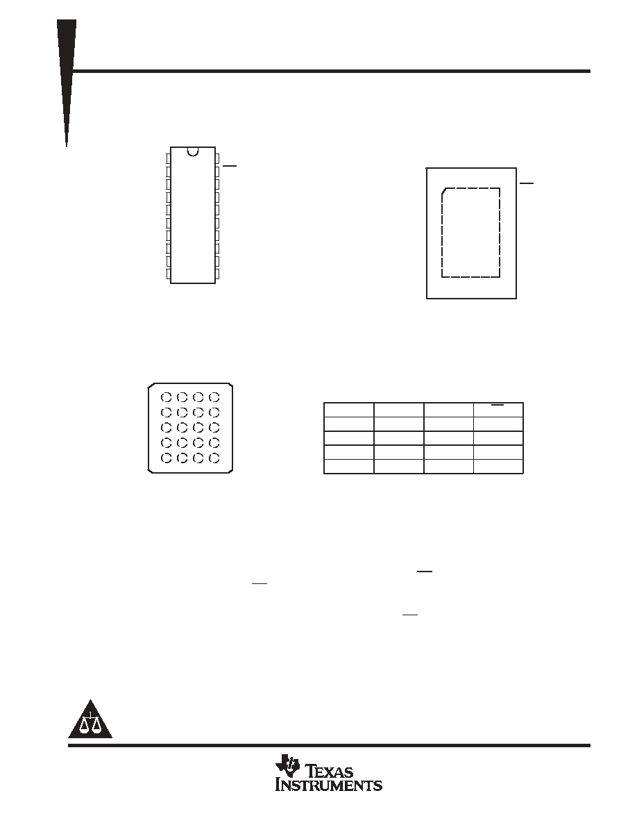
Standard '245-Type Pinout
D
5-
Switch Connection Between Two Ports
D
TTL-Compatible Input Levels
1
2
3
4
5
6
7
8
9
10
20
19
18
17
16
15
14
13
12
11
NC
A1
A2
A3
A4
A5
A6
A7
A8
GND
V
CC
OE
B1
B2
B3
B4
B5
B6
B7
B8
DB, DBQ, DGV, DW, OR PW PACKAGE
(TOP VIEW)
NC - No internal connection
RGY PACKAGE
(TOP VIEW)
1
20
10
11
2
3
4
5
6
7
8
9
19
18
17
16
15
14
13
12
OE
B1
B2
B3
B4
B5
B6
B7
A1
A2
A3
A4
A5
A6
A7
A8
B8
V
GND
CC
NC
NC - No internal connection
terminal assignments
1
2
3
4
A
A1
NC
VCC
OE
B
A3
B2
A2
B1
C
A5
A4
B4
B3
D
A7
B6
A6
B5
E
GND
A8
B8
B7
NC - No internal connection
description/ordering information
The SN74CBT3245A provides eight bits of high-speed TTL-compatible bus switching. The SOIC, SSOP,
TSSOP, and TVSOP packages provide a standard '245 device pinout. The low on-state resistance of the switch
allows connections to be made with minimal propagation delay.
The device is organized as one 8-bit switch. When the output-enable (OE) input is low, the switch is on, and
port A is connected to port B. When OE is high, the switch is open, and the high-impedance state exists between
the two ports.
To ensure the high-impedance state during power up or power down, OE should be tied to V
CC
through a pullup
resistor; the minimum value of the resistor is determined by the current-sinking capability of the driver.
PRODUCTION DATA information is current as of publication date.
Products conform to specifications per the terms of Texas Instruments
standard warranty. Production processing does not necessarily include
testing of all parameters.
Copyright
2004, Texas Instruments Incorporated
Please be aware that an important notice concerning availability, standard warranty, and use in critical applications of
Texas Instruments semiconductor products and disclaimers thereto appears at the end of this data sheet.
GQN OR ZQN PACKAGE
(TOP VIEW)
1
2
3
4
A
B
C
D
E
SN74CBT3245A
OCTAL FET BUS SWITCH
SCDS002Q - NOVEMBER 1992 - REVISED DECEMBER 2004
2
POST OFFICE BOX 655303
∑
DALLAS, TEXAS 75265
description/ordering information (continued)
ORDERING INFORMATION
TA
PACKAGE
ORDERABLE
PART NUMBER
TOP-SIDE
MARKING
QFN - RGY
Tape and reel
SN74CBT3245ARGYR
CU245A
SOIC - DW
Tube
SN74CBT3245ADW
CBT3245A
SOIC - DW
Tape and reel
SN74CBT3245ADWR
CBT3245A
SSOP - DB
Tape and reel
SN74CBT3245ADBR
CU245A
-40
∞
C to 85
∞
C
SSOP (QSOP) - DBQ
Tape and reel
SN74CBT3245ADBQR
CBT3245A
-40
∞
C to 85
∞
C
TSSOP - PW
Tube
SN74CBT3245APW
CU245A
TSSOP - PW
Tape and reel
SN74CBT3245APWR
CU245A
TVSOP - DGV
Tape and reel
SN74CBT3245ADGVR
CU245A
VFBGA - GQN
Tape and reel
SN74CBT3245AGQNR
CU245A
VFBGA - ZQN (Pb-free)
Tape and reel
SN74CBT3245AZQNR
CU245A
Package drawings, standard packing quantities, thermal data, symbolization, and PCB design guidelines are
available at www.ti.com/sc/package.
FUNCTION TABLE
INPUT
FUNCTION
INPUT
OE
FUNCTION
L
A port = B port
H
Disconnect
logic diagram (positive logic)
OE
A1
A8
B1
B8
2
9
19
18
11
Pin numbers shown are for the DB, DBQ, DGV, DW, PW, and RGY packages.
SN74CBT3245A
OCTAL FET BUS SWITCH
SCDS002Q - NOVEMBER 1992 - REVISED DECEMBER 2004
3
POST OFFICE BOX 655303
∑
DALLAS, TEXAS 75265
absolute maximum ratings over operating free-air temperature range (unless otherwise noted)
Supply voltage range, V
CC
-0.5 V to 7 V
. . . . . . . . . . . . . . . . . . . . . . . . . . . . . . . . . . . . . . . . . . . . . . . . . . . . . . . . . .
Input voltage range, V
I
(see Note 1)
-0.5 V to 7 V
. . . . . . . . . . . . . . . . . . . . . . . . . . . . . . . . . . . . . . . . . . . . . . . . . .
Continuous channel current
128 mA
. . . . . . . . . . . . . . . . . . . . . . . . . . . . . . . . . . . . . . . . . . . . . . . . . . . . . . . . . . . . . .
Input clamp current, I
IK
(V
I/O
< 0)
-50 mA
. . . . . . . . . . . . . . . . . . . . . . . . . . . . . . . . . . . . . . . . . . . . . . . . . . . . . . . . .
Package thermal impedance,
JA
(see Note 2): DB package
70
∞
C/W
. . . . . . . . . . . . . . . . . . . . . . . . . . . . . . . . . .
(see Note 2): DBQ package
68
∞
C/W
. . . . . . . . . . . . . . . . . . . . . . . . . . . . . . . .
(see Note 2): DGV package
92
∞
C/W
. . . . . . . . . . . . . . . . . . . . . . . . . . . . . . . .
(see Note 2): DW package
58
∞
C/W
. . . . . . . . . . . . . . . . . . . . . . . . . . . . . . . . .
(see Note 2): GQN/ZQN package
78
∞
C/W
. . . . . . . . . . . . . . . . . . . . . . . . . . .
(see Note 2): PW package
83
∞
C/W
. . . . . . . . . . . . . . . . . . . . . . . . . . . . . . . . .
(see Note 3): RGY package
37
∞
C/W
. . . . . . . . . . . . . . . . . . . . . . . . . . . . . . . .
Storage temperature range, T
stg
-65
∞
C to 150
∞
C
. . . . . . . . . . . . . . . . . . . . . . . . . . . . . . . . . . . . . . . . . . . . . . . . . . .
Stresses beyond those listed under "absolute maximum ratings" may cause permanent damage to the device. These are stress ratings only, and
functional operation of the device at these or any other conditions beyond those indicated under "recommended operating conditions" is not
implied. Exposure to absolute-maximum-rated conditions for extended periods may affect device reliability.
NOTES:
1. The input and output negative-voltage ratings may be exceeded if the input and output clamp-current ratings are observed.
2. The package thermal impedance is calculated in accordance with JESD 51-7.
3. The package thermal impedance is calculated in accordance with JESD 51-5.
recommended operating conditions (see Note 4)
MIN
MAX
UNIT
VCC
Supply voltage
4
5.5
V
VIH
High-level control input voltage
2
V
VIL
Low-level control input voltage
0.8
V
TA
Operating free-air temperature
-40
85
∞
C
NOTE 4: All unused control inputs of the device must be held at VCC or GND to ensure proper device operation. Refer to the TI application report,
Implications of Slow or Floating CMOS Inputs, literature number SCBA004.
electrical characteristics over recommended operating free-air temperature range (unless
otherwise noted)
PARAMETER
TEST CONDITIONS
MIN
TYP
MAX
UNIT
VIK
VCC = 4.5 V,
II = -18 mA
-1.2
V
II
VCC = 5.5 V,
VI = 5.5 V or GND
±
5
µ
A
ICC
VCC = 5.5 V,
IO = 0,
VI = VCC or GND
50
µ
A
ICCß
Control inputs
VCC = 5.5 V,
One input at 3.4 V,
Other inputs at VCC or GND
3.5
mA
Ci
Control inputs
VI = 3 V or 0
4
pF
Cio(OFF)
VO = 3 V or 0,
OE = VCC
4
pF
VI = 0
II = 64 mA
5
7
ron∂
VCC = 4.5 V
VI = 0
II = 30 mA
5
7
ron
VCC = 4.5 V
VI = 2.4 V,
II = 15 mA
10
15
All typical values are at VCC = 5 V (unless otherwise noted), TA = 25
∞
C.
ß This is the increase in supply current for each input that is at the specified TTL voltage level, rather than VCC or GND.
∂ Measured by the voltage drop between the A and B terminals at the indicated current through the switch. On-state resistance is determined by
the lowest voltage of the two (A or B) terminals.
SN74CBT3245A
OCTAL FET BUS SWITCH
SCDS002Q - NOVEMBER 1992 - REVISED DECEMBER 2004
4
POST OFFICE BOX 655303
∑
DALLAS, TEXAS 75265
switching characteristics over recommended operating free-air temperature range, C
L
= 50 pF
(unless otherwise noted) (see Figure 1)
PARAMETER
FROM
(INPUT)
TO
(OUTPUT)
VCC = 4 V
VCC = 5 V
±
0.5 V
UNIT
PARAMETER
(INPUT)
(OUTPUT)
MIN
MAX
MIN
MAX
UNIT
tpd
A or B
B or A
0.35
0.25
ns
ten
OE
A or B
6.4
1.9
5.9
ns
tdis
OE
A or B
5.7
2.1
6
ns
The propagation delay is the calculated RC time constant of the typical on-state resistance of the switch and the specified load capacitance, when
driven by an ideal voltage source (zero output impedance).
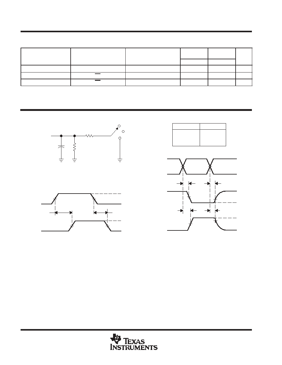
PARAMETER MEASUREMENT INFORMATION
VOH
VOL
From Output
Under Test
CL = 50 pF
(see Note A)
LOAD CIRCUIT
S1
7 V
Open
GND
500
500
tPLH
tPHL
Output
Control
Output
Waveform 1
S1 at 7 V
(see Note B)
Output
Waveform 2
S1 at Open
(see Note B)
tPZL
tPZH
tPLZ
tPHZ
1.5 V
1.5 V
1.5 V
1.5 V
3 V
0 V
1.5 V
1.5 V
VOH
VOL
0 V
1.5 V
VOL + 0.3 V
1.5 V
VOH - 0.3 V
0 V
Input
3 V
3.5 V
VOLTAGE WAVEFORMS
PROPAGATION DELAY TIMES
VOLTAGE WAVEFORMS
ENABLE AND DISABLE TIMES
Output
tpd
tPLZ/tPZL
tPHZ/tPZH
Open
7 V
Open
TEST
S1
NOTES: A. CL includes probe and jig capacitance.
B. Waveform 1 is for an output with internal conditions such that the output is low, except when disabled by the output control.
Waveform 2 is for an output with internal conditions such that the output is high, except when disabled by the output control.
C. All input pulses are supplied by generators having the following characteristics: PRR
10 MHz, ZO = 50
, tr
2.5 ns,
tf
2.5 ns.
D. The outputs are measured one at a time, with one transition per measurement.
E. tPLZ and tPHZ are the same as tdis.
F. tPZL and tPZH are the same as ten.
G. tPLH and tPHL are the same as tpd.
H. All parameters and waveforms are not applicable to all devices.
Figure 1. Load Circuit and Voltage Waveforms
PACKAGING INFORMATION
Orderable Device
Status
(1)
Package
Type
Package
Drawing
Pins Package
Qty
Eco Plan
(2)
Lead/Ball Finish
MSL Peak Temp
(3)
SN74CBT3245ADBLE
OBSOLETE
SSOP
DB
20
TBD
Call TI
Call TI
SN74CBT3245ADBQR
ACTIVE
SSOP/
QSOP
DBQ
20
2500 Green (RoHS &
no Sb/Br)
CU NIPDAU
Level-2-260C-1YEAR
SN74CBT3245ADBQRE4
ACTIVE
SSOP/
QSOP
DBQ
20
2500 Green (RoHS &
no Sb/Br)
CU NIPDAU
Level-2-260C-1YEAR
SN74CBT3245ADBR
ACTIVE
SSOP
DB
20
2000 Green (RoHS &
no Sb/Br)
CU NIPDAU
Level-1-260C-UNLIM
SN74CBT3245ADBRE4
ACTIVE
SSOP
DB
20
2000 Green (RoHS &
no Sb/Br)
CU NIPDAU
Level-1-260C-UNLIM
SN74CBT3245ADGVR
ACTIVE
TVSOP
DGV
20
2000 Green (RoHS &
no Sb/Br)
CU NIPDAU
Level-1-260C-UNLIM
SN74CBT3245ADGVRE4
ACTIVE
TVSOP
DGV
20
2000 Green (RoHS &
no Sb/Br)
CU NIPDAU
Level-1-260C-UNLIM
SN74CBT3245ADW
ACTIVE
SOIC
DW
20
25
Green (RoHS &
no Sb/Br)
CU NIPDAU
Level-1-260C-UNLIM
SN74CBT3245ADWE4
ACTIVE
SOIC
DW
20
25
Green (RoHS &
no Sb/Br)
CU NIPDAU
Level-1-260C-UNLIM
SN74CBT3245ADWR
ACTIVE
SOIC
DW
20
2000 Green (RoHS &
no Sb/Br)
CU NIPDAU
Level-1-260C-UNLIM
SN74CBT3245ADWRE4
ACTIVE
SOIC
DW
20
2000 Green (RoHS &
no Sb/Br)
CU NIPDAU
Level-1-260C-UNLIM
SN74CBT3245AGQNR
ACTIVE
VFBGA
GQN
20
1000
TBD
SNPB
Level-1-240C-UNLIM
SN74CBT3245APW
ACTIVE
TSSOP
PW
20
70
Green (RoHS &
no Sb/Br)
CU NIPDAU
Level-1-260C-UNLIM
SN74CBT3245APWE4
ACTIVE
TSSOP
PW
20
70
Green (RoHS &
no Sb/Br)
CU NIPDAU
Level-1-260C-UNLIM
SN74CBT3245APWLE
OBSOLETE
TSSOP
PW
20
TBD
Call TI
Call TI
SN74CBT3245APWR
ACTIVE
TSSOP
PW
20
2000 Green (RoHS &
no Sb/Br)
CU NIPDAU
Level-1-260C-UNLIM
SN74CBT3245APWRG4
ACTIVE
TSSOP
PW
20
2000 Green (RoHS &
no Sb/Br)
CU NIPDAU
Level-1-260C-UNLIM
SN74CBT3245ARGYR
ACTIVE
QFN
RGY
20
1000 Green (RoHS &
no Sb/Br)
CU NIPDAU
Level-2-260C-1YEAR
SN74CBT3245ARGYRG4
ACTIVE
QFN
RGY
20
1000 Green (RoHS &
no Sb/Br)
CU NIPDAU
Level-2-260C-1YEAR
SN74CBT3245AZQNR
ACTIVE
VFBGA
ZQN
20
1000 Green (RoHS &
no Sb/Br)
SNAGCU
Level-1-260C-UNLIM
(1)
The marketing status values are defined as follows:
ACTIVE: Product device recommended for new designs.
LIFEBUY: TI has announced that the device will be discontinued, and a lifetime-buy period is in effect.
NRND: Not recommended for new designs. Device is in production to support existing customers, but TI does not recommend using this part in
a new design.
PREVIEW: Device has been announced but is not in production. Samples may or may not be available.
OBSOLETE: TI has discontinued the production of the device.
(2)
Eco
Plan
-
The
planned
eco-friendly
classification:
Pb-Free
(RoHS)
or
Green
(RoHS
&
no
Sb/Br)
-
please
check
http://www.ti.com/productcontent
for the latest availability information and additional product content details.
TBD: The Pb-Free/Green conversion plan has not been defined.
Pb-Free (RoHS): TI's terms "Lead-Free" or "Pb-Free" mean semiconductor products that are compatible with the current RoHS requirements
for all 6 substances, including the requirement that lead not exceed 0.1% by weight in homogeneous materials. Where designed to be soldered
PACKAGE OPTION ADDENDUM
www.ti.com
4-Oct-2005
Addendum-Page 1