SN74LVC4245A
OCTAL BUS TRANSCEIVER AND 3.3-V TO 5-V SHIFTER
WITH 3-STATE OUTPUTS
SCAS375G ≠ MARCH 1994 ≠ REVISED AUGUST 2003
1
POST OFFICE BOX 655303
∑
DALLAS, TEXAS 75265
D
Bidirectional Voltage Translator
D
5.5 V on A Port and 2.7 V to 3.6 V on B Port
D
Latch-Up Performance Exceeds 250 mA Per
JESD 17
D
ESD Protection Exceeds JESD 22
≠ 2000-V Human-Body Model (A114-A)
≠ 200-V Machine Model (A115-A)
≠ 1000-V Charged-Device Model (C101)
description/ordering information
This 8-bit (octal) noninverting bus transceiver
contains two separate supply rails; B port has
V
CCB
, which is set at 3.3 V, and A port has V
CCA
,
which is set at 5 V. This allows for translation from
a 3.3-V to a 5-V environment, and vice versa.
The SN74LVC4245A is designed for asynchronous communication between data buses. The device transmits
data from the A bus to the B bus or from the B bus to the A bus, depending on the logic level at the
direction-control (DIR) input. The output-enable (OE) input can be used to disable the device so the buses are
effectively isolated.
The SN74LVC4245A pinout allows the designer to switch to a normal all-3.3-V or all-5-V 20-pin '245 device
without board re-layout. The designer uses the data paths for pins 2 ≠11 and 14 ≠23 of the SN74LVC4245A to
align with the conventional '245 pinout.
ORDERING INFORMATION
TA
PACKAGE
ORDERABLE
PART NUMBER
TOP-SIDE
MARKING
≠40 C to 85 C
SOIC ≠ DW
Tube of 25
SN74LVC4245ADW
LVC4245A
≠40 C to 85 C
SOIC ≠ DW
Reel of 2000
SN74LVC4245ADWR
LVC4245A
≠40
∞
C to 85
∞
C
SSOP ≠ DB
Reel of 2000
SN74LVC4245ADBR
LJ245A
≠40
∞
C to 85
∞
C
TSSOP ≠ PW
Tube of 60
SN74LVC4245APW
LJ245A
TSSOP ≠ PW
Reel of 2000
SN74LVC4245APWR
LJ245A
Reel of 250
SN74LVC4245APWT
Package drawings, standard packing quantities, thermal data, symbolization, and PCB design
guidelines are available at www.ti.com/sc/package.
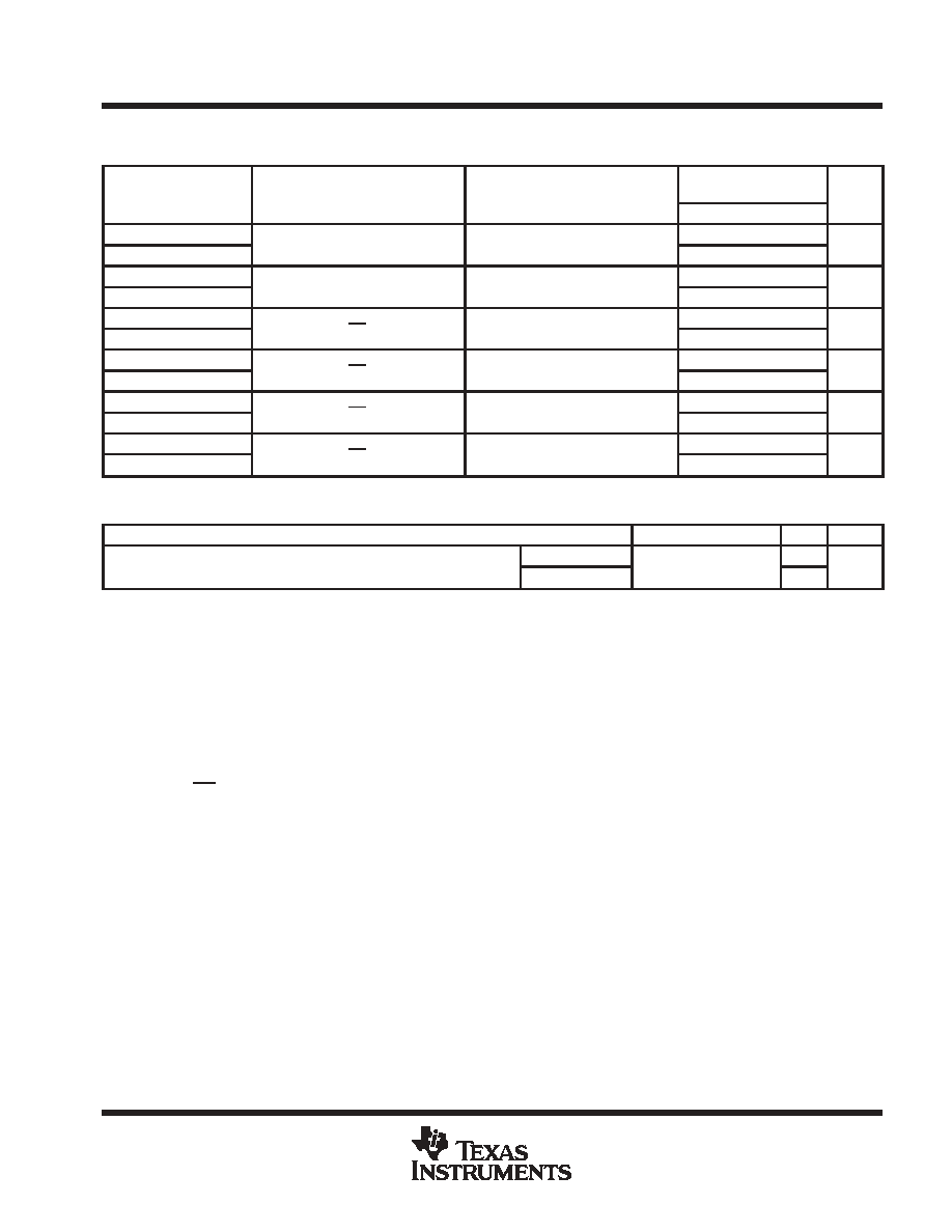
FUNCTION TABLE
INPUTS
OPERATION
OE
DIR
OPERATION
L
L
B data to A bus
L
H
A data to B bus
H
X
Isolation
Copyright
2003, Texas Instruments Incorporated
Please be aware that an important notice concerning availability, standard warranty, and use in critical applications of
Texas Instruments semiconductor products and disclaimers thereto appears at the end of this data sheet.
PRODUCTION DATA information is current as of publication date.
Products conform to specifications per the terms of Texas Instruments
standard warranty. Production processing does not necessarily include
testing of all parameters.
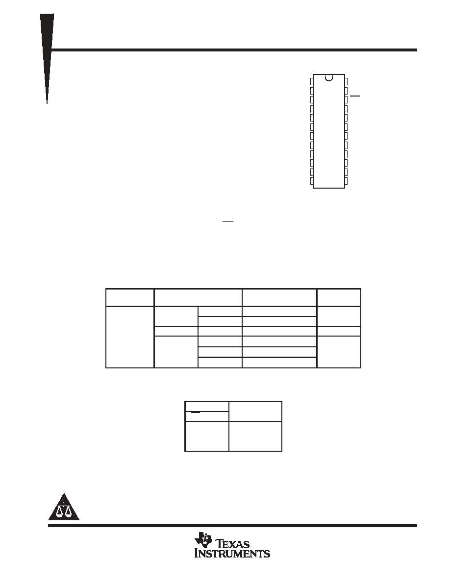
DB, DW, OR PW PACKAGE
(TOP VIEW)
1
2
3
4
5
6
7
8
9
10
11
12
24
23
22
21
20
19
18
17
16
15
14
13
(5 V) V
CCA
DIR
A1
A2
A3
A4
A5
A6
A7
A8
GND
GND
V
CCB
(3.3 V)
V
CCB
(3.3 V)
OE
B1
B2
B3
B4
B5
B6
B7
B8
GND
SN74LVC4245A
OCTAL BUS TRANSCEIVER AND 3.3-V TO 5-V SHIFTER
WITH 3-STATE OUTPUTS
SCAS375G ≠ MARCH 1994 ≠ REVISED AUGUST 2003
2
POST OFFICE BOX 655303
∑
DALLAS, TEXAS 75265
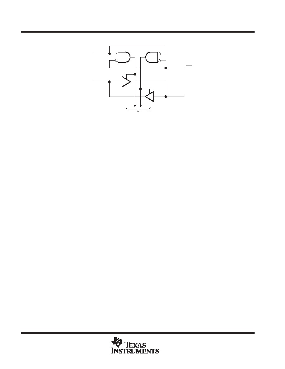
logic diagram (positive logic)
DIR
OE
A1
B1
To Seven Other Channels
2
3
22
21
absolute maximum ratings over operating free-air temperature range for V
CCA
= 4.5 V to 5.5 V
(unless otherwise noted)
Supply voltage range, V
CCA
≠0.5 V to 6.5 V
. . . . . . . . . . . . . . . . . . . . . . . . . . . . . . . . . . . . . . . . . . . . . . . . . . . . . . . .
Input voltage range, V
I
: A port (see Note 1)
≠0.5 V to V
CCA
+ 0.5 V
. . . . . . . . . . . . . . . . . . . . . . . . . . . . . . . . . . .
Control inputs
≠0.5 V to 6 V
. . . . . . . . . . . . . . . . . . . . . . . . . . . . . . . . . . . . . . . . . . . . . . . .
Output voltage range, V
O
: A port (see Note 1)
≠0.5 V to V
CCA
+ 0.5 V
. . . . . . . . . . . . . . . . . . . . . . . . . . . . . . . .
Input clamp current, I
IK
(V
I
< 0)
≠50 mA
. . . . . . . . . . . . . . . . . . . . . . . . . . . . . . . . . . . . . . . . . . . . . . . . . . . . . . . . . . .
Output clamp current, I
OK
(V
O
< 0)
≠50 mA
. . . . . . . . . . . . . . . . . . . . . . . . . . . . . . . . . . . . . . . . . . . . . . . . . . . . . . . .
Continuous output current, I
O
±
50 mA
. . . . . . . . . . . . . . . . . . . . . . . . . . . . . . . . . . . . . . . . . . . . . . . . . . . . . . . . . . . . .
Continuous current through each V
CCA
or GND
±
100 mA
. . . . . . . . . . . . . . . . . . . . . . . . . . . . . . . . . . . . . . . . . . .
Package thermal impedance,
JA
(see Note 2): DB package
63
∞
C/W
. . . . . . . . . . . . . . . . . . . . . . . . . . . . . . . . .
DW package
46
∞
C/W
. . . . . . . . . . . . . . . . . . . . . . . . . . . . . . . . .
PW package
88
∞
C/W
. . . . . . . . . . . . . . . . . . . . . . . . . . . . . . . . .
Storage temperature range, T
stg
≠65
∞
C to 150
∞
C
. . . . . . . . . . . . . . . . . . . . . . . . . . . . . . . . . . . . . . . . . . . . . . . . . . .
Stresses beyond those listed under "absolute maximum ratings" may cause permanent damage to the device. These are stress ratings only, and
functional operation of the device at these or any other conditions beyond those indicated under "recommended operating conditions" is not
implied. Exposure to absolute-maximum-rated conditions for extended periods may affect device reliability.
NOTES:
1. This value is limited to 6 V maximum.
2. The package thermal impedance is calculated in accordance with JESD 51-7.
SN74LVC4245A
OCTAL BUS TRANSCEIVER AND 3.3-V TO 5-V SHIFTER
WITH 3-STATE OUTPUTS
SCAS375G ≠ MARCH 1994 ≠ REVISED AUGUST 2003
3
POST OFFICE BOX 655303
∑
DALLAS, TEXAS 75265
absolute maximum ratings over operating free-air temperature range for V
CCB
= 2.7 V to 3.6 V
(unless otherwise noted)
Supply voltage range, V
CCB
≠0.5 V to 4.6 V
. . . . . . . . . . . . . . . . . . . . . . . . . . . . . . . . . . . . . . . . . . . . . . . . . . . . . . . .
Input voltage range, V
I
: B port (see Note 3)
≠0.5 V to V
CCB
+ 0.5 V
. . . . . . . . . . . . . . . . . . . . . . . . . . . . . . . . . . .
Output voltage range, V
O
:
B port (see Note 3)
≠0.5 V to V
CCB
+ 0.5 V
. . . . . . . . . . . . . . . . . . . . . . . . . . . . . . . .
Input clamp current, I
IK
(V
I
< 0)
≠50 mA
. . . . . . . . . . . . . . . . . . . . . . . . . . . . . . . . . . . . . . . . . . . . . . . . . . . . . . . . . . .
Output clamp current, I
OK
(V
O
< 0)
≠50 mA
. . . . . . . . . . . . . . . . . . . . . . . . . . . . . . . . . . . . . . . . . . . . . . . . . . . . . . . .
Continuous output current, I
O
±
50 mA
. . . . . . . . . . . . . . . . . . . . . . . . . . . . . . . . . . . . . . . . . . . . . . . . . . . . . . . . . . . . .
Continuous current through V
CCB
or GND
±
100 mA
. . . . . . . . . . . . . . . . . . . . . . . . . . . . . . . . . . . . . . . . . . . . . . . .
Package thermal impedance,
JA
(see Note 2): DB package
63
∞
C/W
. . . . . . . . . . . . . . . . . . . . . . . . . . . . . . . . .
DW package
46
∞
C/W
. . . . . . . . . . . . . . . . . . . . . . . . . . . . . . . . .
PW package
88
∞
C/W
. . . . . . . . . . . . . . . . . . . . . . . . . . . . . . . . .
Storage temperature range, T
stg
≠65
∞
C to 150
∞
C
. . . . . . . . . . . . . . . . . . . . . . . . . . . . . . . . . . . . . . . . . . . . . . . . . . .
Stresses beyond those listed under "absolute maximum ratings" may cause permanent damage to the device. These are stress ratings only, and
functional operation of the device at these or any other conditions beyond those indicated under "recommended operating conditions" is not
implied. Exposure to absolute-maximum-rated conditions for extended periods may affect device reliability.
NOTES:
2. The package thermal impedance is calculated in accordance with JESD 51-7.
3. This value is limited to 4.6 V maximum.
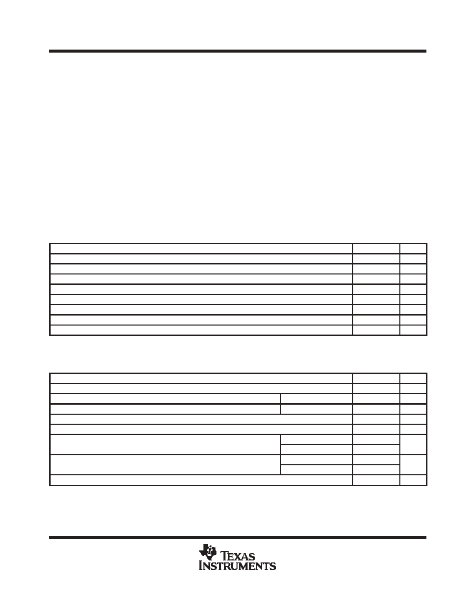
recommended operating conditions for V
CCA
= 4.5 V to 5.5 V (see Note 4)
MIN
MAX
UNIT
VCCA
Supply voltage
4.5
5.5
V
VIH
High-level input voltage
2
V
VIL
Low-level input voltage
0.8
V
VI
Input voltage
0
VCCA
V
VO
Output voltage
0
VCCA
V
IOH
High-level output current
≠24
mA
IOL
Low-level output current
24
mA
TA
Operating free-air temperature
≠40
85
∞
C
NOTE 4: All unused inputs of the device must be held at the associated VCC or GND to ensure proper device operation. Refer to the TI application
report, Implications of Slow or Floating CMOS Inputs, literature number SCBA004.
recommended operating conditions for V
CCB
= 2.7 V to 3.6 V (see Note 4)
MIN
MAX
UNIT
VCCB
Supply voltage
2.7
3.6
V
VIH
High-level input voltage
VCCB = 2.7 V to 3.6 V
2
V
VIL
Low-level input voltage
VCCB = 2.7 V to 3.6 V
0.8
V
VI
Input voltage
0
VCCB
V
VO
Output voltage
0
VCCB
V
IOH
High-level output current
VCCB = 2.7 V
≠12
mA
IOH
High-level output current
VCCB = 3 V
≠24
mA
IOL
Low-level output current
VCCB = 2.7 V
12
mA
IOL
Low-level output current
VCCB = 3 V
24
mA
TA
Operating free-air temperature
≠40
85
∞
C
NOTE 4: All unused inputs of the device must be held at the associated VCC or GND to ensure proper device operation. Refer to the TI application
report, Implications of Slow or Floating CMOS Inputs, literature number SCBA004.
SN74LVC4245A
OCTAL BUS TRANSCEIVER AND 3.3-V TO 5-V SHIFTER
WITH 3-STATE OUTPUTS
SCAS375G ≠ MARCH 1994 ≠ REVISED AUGUST 2003
4
POST OFFICE BOX 655303
∑
DALLAS, TEXAS 75265
electrical characteristics over recommended operating free-air temperature range for
V
CCA
= 4.5 V to 5.5 V (unless otherwise noted) (see Note 5)
PARAMETER
TEST CONDITIONS
VCCA
MIN
TYP
MAX
UNIT
V
IOH = ≠100
µ
A
4.5 V
4.3
V
VOH
IOH = ≠100
µ
A
5.5 V
5.3
V
VOH
IOH = ≠24 mA
4.5 V
3.7
V
IOH = ≠24 mA
5.5 V
4.7
V
IOL = 100
µ
A
4.5 V
0.2
V
VOL
IOL = 100
µ
A
5.5 V
0.2
V
VOL
IOL = 24 mA
4.5 V
0.55
V
IOL = 24 mA
5.5 V
0.55
II
Control inputs
VI = VCCA or GND
5.5 V
±
1
µ
A
IOZ
A port
VO = VCCA or GND
5.5 V
±
5
µ
A
ICCA
VI = VCCA or GND,
IO = 0
5.5 V
80
µ
A
ICCAß
One input at 3.4 V,
Other inputs at VCCA or GND
5.5 V
1.5
mA
Ci
Control inputs
VI = VCCA or GND
Open
5
pF
Cio
A port
VO = VCCA or GND
5 V
11
pF
All typical values are measured at VCC = 5 V, TA = 25
∞
C.
For I/O ports, the parameter IOZ includes the input leakage current.
ß This is the increase in supply current for each input that is at one of the specified TTL voltage levels, rather than 0 V or the associated VCC.
NOTE 5: VCCB = 2.7 V to 3.6 V
electrical characteristics over recommended operating free-air temperature range for
V
CCB
= 2.7 V to 3.6 V (unless otherwise noted) (see Note 6)
PARAMETER
TEST CONDITIONS
VCCB
MIN
TYP∂
MAX
UNIT
V
IOH = ≠100
µ
A
2.7 V to 3.6 V
VCC≠0.2
V
VOH
IOH = ≠12 mA
2.7 V
2.2
V
VOH
IOH = ≠12 mA
3 V
2.4
V
IOH = ≠24 mA
3 V
2
V
IOL = 100
µ
A
2.7 V to 3.6 V
0.2
V
VOL
IOL = 12 mA
2.7 V
0.4
V
OL
IOL = 24 mA
3 V
0.55
IOZ
B port
VO = VCCB or GND
3.6 V
±
5
µ
A
ICCB
VI = VCCB or GND,
IO = 0
3.6 V
50
µ
A
ICCBß
One input at VCCB ≠ 0.6 V,
Other inputs at VCCB or GND
2.7 V to 3.6 V
0.5
mA
Cio
B port
VO = VCCB or GND
3.3 V
11
pF
For I/O ports, the parameter IOZ includes the input leakage current.
ß This is the increase in supply current for each input that is at one of the specified TTL voltage levels, rather than 0 V or the associated VCC.
∂ All typical values are measured at VCC = 3.3 V, TA = 25
∞
C.
NOTE 6: VCCA = 5 V
±
0.5 V
SN74LVC4245A
OCTAL BUS TRANSCEIVER AND 3.3-V TO 5-V SHIFTER
WITH 3-STATE OUTPUTS
SCAS375G ≠ MARCH 1994 ≠ REVISED AUGUST 2003
5
POST OFFICE BOX 655303
∑
DALLAS, TEXAS 75265
switching characteristics over recommended operating free-air temperature range, C
L
= 50 pF
(unless otherwise noted) (see Figures 1 and 2)
PARAMETER
FROM
(INPUT)
TO
(OUTPUT)
VCCA = 5 V
±
0.5 V,
VCCB = 2.7 V TO 3.6 V
UNIT
PARAMETER
(INPUT)
(OUTPUT)
MIN
MAX
UNIT
tPHL
A
B
1
6.3
ns
tPLH
A
B
1
6.7
ns
tPHL
B
A
1
6.1
ns
tPLH
B
A
1
5
ns
tPZL
OE
A
1
9
ns
tPZH
OE
A
1
8.1
ns
tPZL
OE
B
1
8.8
ns
tPZH
OE
B
1
9.8
ns
tPLZ
OE
A
1
7
ns
tPHZ
OE
A
1
5.8
ns
tPLZ
OE
B
1
7.7
ns
tPHZ
OE
B
1
7.8
ns
operating characteristics, V
CCA
= 4.5 V to 5.5 V, V
CCB
= 2.7 V to 3.6 V, T
A
= 25
∞
C
PARAMETER
TEST CONDITIONS
TYP
UNIT
Cpd
Power dissipation capacitance per transceiver
Outputs enabled
CL = 0,
f = 10 MHz
39.5
pF
Cpd
Power dissipation capacitance per transceiver
Outputs disabled
CL = 0,
f = 10 MHz
5
pF
power-up considerations
TI level-translation devices offer an opportunity for successful mixed-voltage signal design. A proper power-up
sequence always should be followed to avoid excessive supply current, bus contention, oscillations, or other
anomalies caused by improperly biased device pins. Take these precautions to guard against such power-up
problems.
1.
Connect ground before any supply voltage is applied.
2.
Next, power up the control side of the device (V
CCA
for all four of these devices).
3.
Tie OE to V
CCA
with a pullup resistor so that it ramps with V
CCA
.
4.
Depending on the direction of the data path, DIR can be high or low. If DIR high is needed (A data to B bus),
ramp it with V
CCA
. Otherwise, keep DIR low.
Refer to the TI application report, Texas Instruments Voltage-Level-Translation Devices, literature number SCEA021.