Äîêóìåíòàöèÿ è îïèñàíèÿ www.docs.chipfind.ru
SN54LVT162240, SN74LVT162240
3.3-V ABT 16-BIT BUFFERS/DRIVERS
WITH 3-STATE OUTPUTS
SCBS719 JULY 2000
1
POST OFFICE BOX 655303
·
DALLAS, TEXAS 75265
D
Members of the Texas Instruments
Widebus
TM
Family
D
State-of-the-Art Advanced BiCMOS
Technology (ABT) Design for 3.3-V
Operation and Low Static-Power
Dissipation
D
Output Ports Have Equivalent 22-
Series
Resistors, So No External Resistors Are
Required
D
Support Mixed-Mode Signal Operation
(5-V Input and Output Voltages With
3.3-V V
CC
)
D
Support Unregulated Battery Operation
Down to 2.7 V
D
Typical V
OLP
(Output Ground Bounce)
<0.8 V at V
CC
= 3.3 V, T
A
= 25
°
C
D
I
off
and Power-Up 3-State Support Hot
Insertion
D
Distributed V
CC
and GND Pins Minimize
High-Speed Switching Noise
D
Flow-Through Architecture Optimizes PCB
Layout
D
Latch-Up Performance Exceeds 100 mA Per
JESD 78, Class II
D
ESD Protection Exceeds JESD 22
2000-V Human-Body Model (A114-A)
200-V Machine Model (A115-A)
1000-V Charged-Device Model (C101)
D
Package Options Include Plastic Shrink
Small-Outline (DL), Thin Shrink
Small-Outline (DGG), and Thin Very
Small-Outline (DGV) Packages and 380-mil
Fine-Pitch Ceramic Flat (WD) Package
Using 25-mil Center-to-Center Spacings
NOTE: For tape and reel order entry:
The DGGR package is abbreviated to GR, and
the DGVR package is abbreviated to VR.
description
The 'LVT162240 devices are 16-bit buffers/drivers designed specifically for low-voltage (3.3-V) V
CC
operation
and to improve both the performance and density of 3-state memory address drivers, clock drivers, and
bus-oriented receivers and transmitters. They have the capability to provide a TTL interface to a 5-V system
environment.
These devices can be used as four 4-bit buffers, two 8-bit buffers, or one 16-bit buffer and provide inverting
outputs and symmetrical active-low output-enable (OE) inputs.
Copyright
©
2000, Texas Instruments Incorporated
UNLESS OTHERWISE NOTED this document contains PRODUCTION
DATA information current as of publication date. Products conform to
specifications per the terms of Texas Instruments standard warranty.
Production processing does not necessarily include testing of all
parameters.
Please be aware that an important notice concerning availability, standard warranty, and use in critical applications of
Texas Instruments semiconductor products and disclaimers thereto appears at the end of this data sheet.
Widebus is a trademark of Texas Instruments.
1
2
3
4
5
6
7
8
9
10
11
12
13
14
15
16
17
18
19
20
21
22
23
24
48
47
46
45
44
43
42
41
40
39
38
37
36
35
34
33
32
31
30
29
28
27
26
25
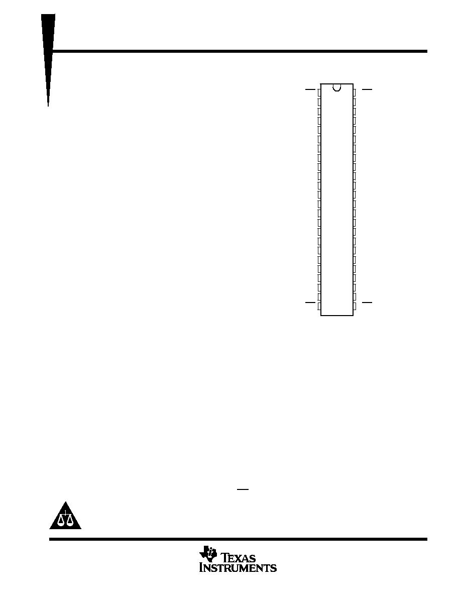
1OE
1Y1
1Y2
GND
1Y3
1Y4
V
CC
2Y1
2Y2
GND
2Y3
2Y4
3Y1
3Y2
GND
3Y3
3Y4
V
CC
4Y1
4Y2
GND
4Y3
4Y4
4OE
2OE
1A1
1A2
GND
1A3
1A4
V
CC
2A1
2A2
GND
2A3
2A4
3A1
3A2
GND
3A3
3A4
V
CC
4A1
4A2
GND
4A3
4A4
3OE
SN54LVT162240 . . . WD PACKAGE
SN74LVT162240 . . . DGG, DGV, OR DL PACKAGE
(TOP VIEW)
SN54LVT162240, SN74LVT162240
3.3-V ABT 16-BIT BUFFERS/DRIVERS
WITH 3-STATE OUTPUTS
SCBS719 JULY 2000
2
POST OFFICE BOX 655303
·
DALLAS, TEXAS 75265
description (continued)
The outputs, which are designed to source or sink up to 12 mA, include equivalent 22-
series resistors to
reduce overshoot and undershoot.
When V
CC
is between 0 and 1.5 V, the devices are in the high-impedance state during power up or power down.
However, to ensure the high-impedance state above 1.5 V, OE should be tied to V
CC
through a pullup resistor;
the minimum value of the resistor is determined by the current-sinking capability of the driver.
These devices are fully specified for hot-insertion applications using I
off
and power-up 3-state. The I
off
circuitry
disables the outputs, preventing damaging current backflow through the devices when they are powered down.
The power-up 3-state circuitry places the outputs in the high-impedance state during power up and power down,
which prevents driver conflict.
The SN54LVT162240 is characterized for operation over the full military temperature range of 55
°
C to 125
°
C.
The SN74LVT162240 is characterized for operation from 40
°
C to 85
°
C.
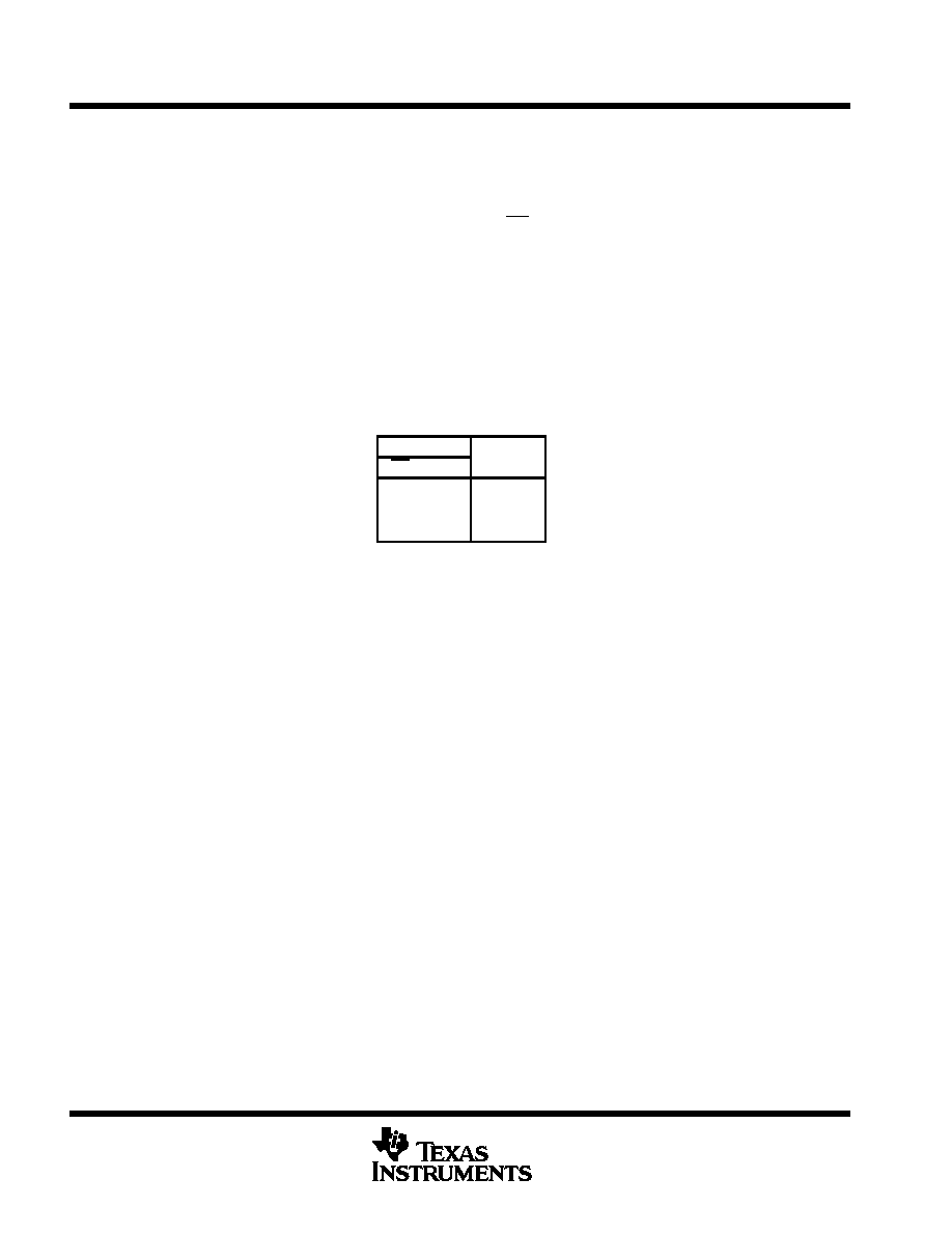
FUNCTION TABLE
(each 4-bit buffer/driver)
INPUTS
OUTPUT
OE
A
Y
L
H
L
L
L
H
H
X
Z
SN54LVT162240, SN74LVT162240
3.3-V ABT 16-BIT BUFFERS/DRIVERS
WITH 3-STATE OUTPUTS
SCBS719 JULY 2000
3
POST OFFICE BOX 655303
·
DALLAS, TEXAS 75265
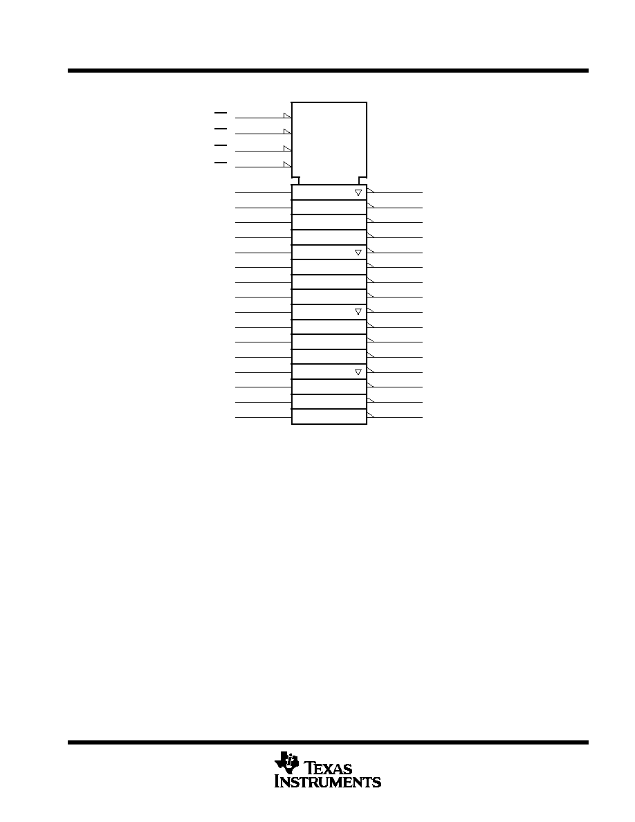
logic symbol
47
1A1
46
1A2
44
1A3
43
1A4
1Y1
2
1Y2
3
1Y3
5
1Y4
6
41
2A1
40
2A2
38
2A3
37
2A4
2Y1
8
2Y2
9
2Y3
11
2Y4
12
36
3A1
35
3A2
33
3A3
32
3A4
3Y1
13
3Y2
14
3Y3
16
3Y4
17
30
4A1
29
4A2
27
4A3
26
4A4
4Y1
19
4Y2
20
4Y3
22
4Y4
23
EN1
1
EN4
24
1OE
2OE
3OE
4OE
EN2
48
EN3
25
1
1
1
2
1
3
1
4
This symbol is in accordance with ANSI/IEEE Std 91-1984 and IEC Publication 617-12.
SN54LVT162240, SN74LVT162240
3.3-V ABT 16-BIT BUFFERS/DRIVERS
WITH 3-STATE OUTPUTS
SCBS719 JULY 2000
4
POST OFFICE BOX 655303
·
DALLAS, TEXAS 75265
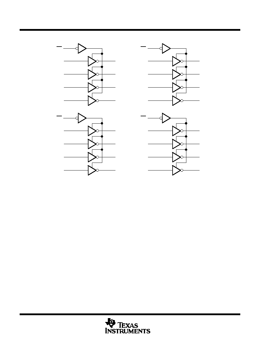
logic diagram (positive logic)
1OE
1A1
1A2
1A3
1A4
1Y1
1Y2
1Y3
1Y4
1
47
46
44
43
2
3
5
6
2OE
2A1
2A2
2A3
2A4
2Y1
2Y2
2Y3
2Y4
48
41
40
38
37
8
9
11
12
3OE
3A1
3A2
3A3
3A4
3Y1
3Y2
3Y3
3Y4
25
36
35
33
32
13
14
16
17
4OE
4A1
4A2
4A3
4A4
4Y1
4Y2
4Y3
4Y4
24
30
29
27
26
19
20
22
23
absolute maximum ratings over operating free-air temperature range (unless otherwise noted)
Supply voltage range, V
CC
0.5 V to 4.6 V
. . . . . . . . . . . . . . . . . . . . . . . . . . . . . . . . . . . . . . . . . . . . . . . . . . . . . . . . .
Input voltage range, V
I
(see Note 1)
0.5 V to 7 V
. . . . . . . . . . . . . . . . . . . . . . . . . . . . . . . . . . . . . . . . . . . . . . . . . .
Voltage range applied to any output in the high-impedance
or power-off state, V
O
(see Note 1)
0.5 V to 7 V
. . . . . . . . . . . . . . . . . . . . . . . . . . . . . . . . . . . . . . . . . . . . . . . .
Voltage range applied to any output in the high state, V
O
(see Note 1)
0.5 V to V
CC
+ 0.5 V
. . . . . . . . . . . . .
Current into any output in the low state, I
O
30
mA
. . . . . . . . . . . . . . . . . . . . . . . . . . . . . . . . . . . . . . . . . . . . . . . . . .
Current into any output in the high state, I
O
(see Note 2)
30 mA
. . . . . . . . . . . . . . . . . . . . . . . . . . . . . . . . . . . . . .
Input clamp current, I
IK
(V
I
< 0)
50 mA
. . . . . . . . . . . . . . . . . . . . . . . . . . . . . . . . . . . . . . . . . . . . . . . . . . . . . . . . . . .
Output clamp current, I
OK
(V
O
< 0)
50 mA
. . . . . . . . . . . . . . . . . . . . . . . . . . . . . . . . . . . . . . . . . . . . . . . . . . . . . . . .
Package thermal impedance,
JA
(see Note 3): DGG package
70
°
C/W
. . . . . . . . . . . . . . . . . . . . . . . . . . . . . . .
DGV package
58
°
C/W
. . . . . . . . . . . . . . . . . . . . . . . . . . . . . . . .
DL package
63
°
C/W
. . . . . . . . . . . . . . . . . . . . . . . . . . . . . . . . .
Storage temperature range, T
stg
65
°
C to 150
°
C
. . . . . . . . . . . . . . . . . . . . . . . . . . . . . . . . . . . . . . . . . . . . . . . . . . .
Stresses beyond those listed under "absolute maximum ratings" may cause permanent damage to the device. These are stress ratings only, and
functional operation of the device at these or any other conditions beyond those indicated under "recommended operating conditions" is not
implied. Exposure to absolute-maximum-rated conditions for extended periods may affect device reliability.
NOTES:
1. The input and output negative-voltage ratings may be exceeded if the input and output clamp-current ratings are observed.
2. This current flows only when the output is in the high state and VO > VCC.
3. The package thermal impedance is calculated in accordance with JESD 51.
SN54LVT162240, SN74LVT162240
3.3-V ABT 16-BIT BUFFERS/DRIVERS
WITH 3-STATE OUTPUTS
SCBS719 JULY 2000
5
POST OFFICE BOX 655303
·
DALLAS, TEXAS 75265
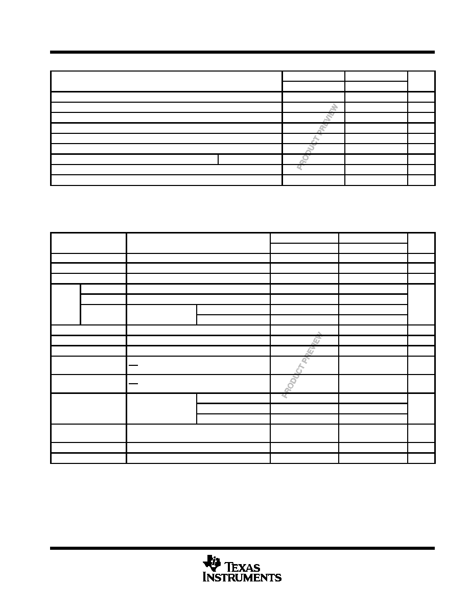
recommended operating conditions (see Note 4)
SN54LVT162240
SN74LVT162240
UNIT
MIN
MAX
MIN
MAX
UNIT
VCC
Supply voltage
2.7
3.6
2.7
3.6
V
VIH
High-level input voltage
2
2
V
VIL
Low-level input voltage
0.8
0.8
V
VI
Input voltage
5.5
5.5
V
IOH
High-level output current
12
12
mA
IOL
Low-level output current
12
12
mA
t/
v
Input transition rise or fall rate
Outputs enabled
10
10
ns/V
t/
VCC
Power-up ramp rate
200
200
µ
s/V
TA
Operating free-air temperature
55
125
40
85
°
C
NOTE 4: All unused inputs of the device must be held at VCC or GND to ensure proper device operation. Refer to the TI application report,
Implications of Slow or Floating CMOS Inputs, literature number SCBA004.
electrical characteristics over recommended operating free-air temperature range (unless
otherwise noted)
PARAMETER
TEST CONDITIONS
SN54LVT162240
SN74LVT162240
UNIT
PARAMETER
TEST CONDITIONS
MIN
TYP
MAX
MIN
TYP
MAX
UNIT
VIK
VCC = 2.7 V,
II = 18 mA
1.2
1.2
V
VOH
VCC = 3 V,
IOH = 12 mA
2
2
V
VOL
VCC = 3 V,
IOL = 12 mA
0.8
0.8
V
VCC = 0 or 3.6 V,
VI = 5.5 V
10
10
II
Control inputs
VCC = 3.6 V,
VI = VCC or GND
±
1
±
1
µ
A
II
Data inp ts
VCC = 3 6 V
VI = VCC
1
1
µ
A
Data inputs
VCC = 3.6 V
VI = 0
5
5
Ioff
VCC = 0,
VI or VO = 0 to 4.5 V
±
100
µ
A
IOZH
VCC = 3.6 V,
VO = 3 V
5
5
µ
A
IOZL
VCC = 3.6 V,
VO = 0.5 V
5
5
µ
A
IOZPU
VCC = 0 to 1.5 V, VO = 0.5 V to 3 V,
OE = don't care
±
100*
±
100
µ
A
IOZPD
VCC = 1.5 V to 0, VO = 0.5 V to 3 V,
OE = don't care
±
100*
±
100
µ
A
VCC = 3.6 V,
Outputs high
0.19
0.19
ICC
VCC = 3.6 V,
IO = 0,
Outputs low
5
5
mA
VI = VCC or GND
Outputs disabled
0.19
0.19
ICC
VCC = 3 V to 3.6 V, One input at VCC 0.6 V,
Other inputs at VCC or GND
0.2
0.2
mA
Ci
VI = 3 V or 0
4
4
pF
Co
VO = 3 V or 0
9
9
pF
On products compliant to MIL-PRF-38535, this parameter is not production tested.
All typical values are at VCC = 3.3 V, TA = 25
°
C.
This is the increase in supply current for each input that is at the specified TTL voltage level rather than VCC or GND.
PRODUCT PREVIEW information concerns products in the formative or
design phase of development. Characteristic data and other
specifications are design goals. Texas Instruments reserves the right to
change or discontinue these products without notice.