 | –≠–ª–µ–∫—Ç—Ä–æ–Ω–Ω—ã–π –∫–æ–º–ø–æ–Ω–µ–Ω—Ç: SN75174DW | –°–∫–∞—á–∞—Ç—å:  PDF PDF  ZIP ZIP |
SN54AS882A, SN74AS882A
32-BIT LOOK-AHEAD CARRY GENERATORS
SDAS235 ≠ D2661, DECEMBER 1982 ≠ REVISED NOVEMBER 1985
POST OFFICE BOX 655303
∑
DALLAS, TEXAS 75265
Copyright
©
1985, Texas Instruments Incorporated
1
∑
Directly Compatible With 'AS181B,
'AS1181, 'AS881B, and 'AS1881 ALUs
∑
Package Options Include Plastic Small
Outline Packages, Both Plastic and
Ceramic Chip Carriers, and Standard
Plastic and Ceramic 300-mil DIPs
∑
Capable of Anticipating the Carry Across a
Group of Eight 4-Bit Binary Adders
∑
Cascadable to Perform Look-Ahead Across
n-Bit Adders
∑
Typical Carry Time, C
n
to Any C
n+i
, is Less
Than 6 ns
∑
Dependable Texas Instruments Quality and
Reliability
description
The 'AS882A is a high-speed look-ahead carry
generator capable of anticipating the carry across
a group of eight 4-bit adders permitting the
designer to implement look-ahead for a 32-bit ALU
with a single package or, by cascading 'AS882As,
full look-ahead is possible across n-bit adders.
The SN54AS882A is characterized for operation
over the full military temperature range of ≠ 55
∞
C
to 125
∞
C. The SN74AS882A is characterized for
operation from 0
∞
C to 70
∞
C.
'AS882A LOGIC EQUATIONS
C
n+8
=
G1 + P1G0+P1P0C
n
C
n+16
=
G3 + P3G2 + P3P2G1 + P3P2P1G0
+ P3P2P1P0C
n
C
n+24
=
G5 + P5G4 + P5P4G3 + P5P4P3G2
+ P5P4P3P2G1 + P5P4P3P2P1G0
+ P5P4P3P2P1P0C
n
C
n+32
=
G7 + P7G6 + P7P6G5 + P7P6P5G4
+ P7P6P5P4G3 + P7P6P5P4P3G2
+ P7P6P5P4P3P2G1 + P7P6P5P4P3P2P1G0
+ P7P6P5P4P3P2P1P0C
n
1
2
3
4
5
6
7
8
9
10
11
12
24
23
22
21
20
19
18
17
16
15
14
13
C
n
G0
P0
G1
P1
C
n + 8
G2
P2
G3
P3
C
n ≠ 16
GND
V
CC
NC
C
n + 32
P7
G7
P6
G6
C
n + 24
P5
G5
P4
G4
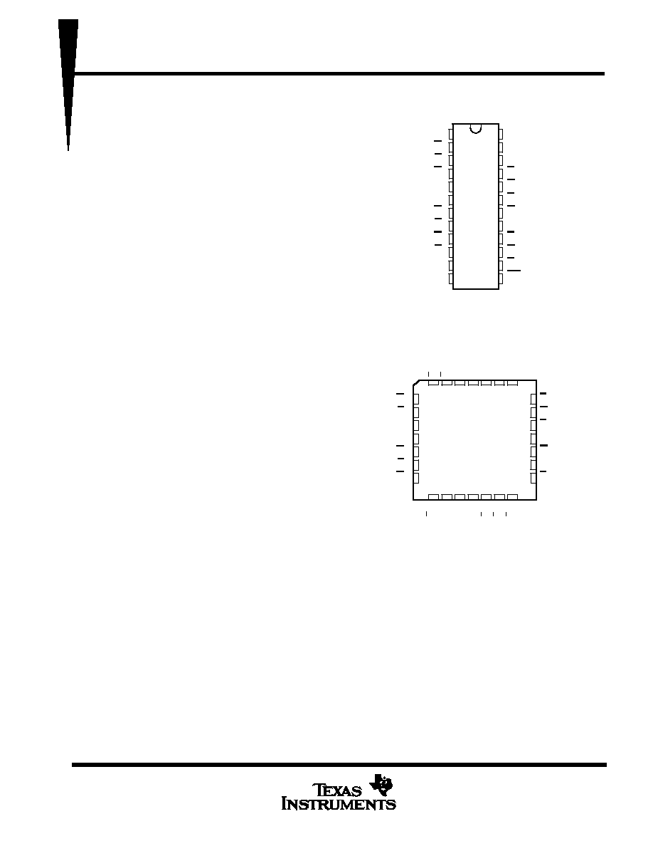
SN54AS882A . . . JT PACKAGE
SN74AS882A . . . DW OR NT PACKAGE
(TOP VIEW)
3 2 1
13 14
5
6
7
8
9
10
11
P7
G7
P6
NC
G6
C
n + 24
P5
G1
P1
C
n + 8
NC
G2
P2
G3
4
15 16 17 18
GND
NC
G4
P4
G5
P0
G0
NC
SN54AS882A . . . FK PACKAGE
SN74AS882A . . . DW OR NT PACKAGE
(TOP VIEW)
28 27 26
25
24
23
22
21
20
19
12
P3
NC
n + 32
C
CC
V
C
n
n + 16
C
NC ≠ No internal connection
PRODUCTION DATA information is current as of publication date.
Products conform to specifications per the terms of Texas Instruments
standard warranty. Production processing does not necessarily include
testing of all parameters.
SN54AS882A, SN74AS882A
32-BIT LOOK-AHEAD CARRY GENERATORS
SDAS235 ≠ D2661, DECEMBER 1982 ≠ REVISED NOVEMBER 1985
POST OFFICE BOX 655303
∑
DALLAS, TEXAS 75265
2
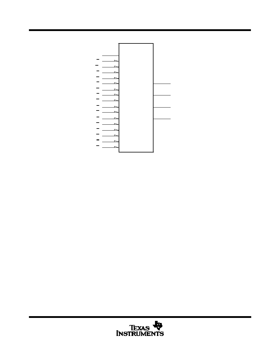
logic symbol
6
Cn+8
Cn+16
11
Cn+24
17
Cn+32
22
CO1
CO3
CO5
CO7
C1
CP0
CG0
CP1
CG1
CP2
CG2
CP3
CG3
CP4
CG4
CP5
CG5
CP6
CG6
CP7
CG7
CPG
G7
P7
G6
P6
G5
P5
G4
P4
G3
P3
G2
P2
G1
P1
GO
P0
Cn
16
14
10
8
4
5
2
3
1
7
9
13
15
19
18
21
20
This symbol is in accordance with ANSI/IEEE Std 91-1984 and IEC Publication 617-12.
Pin numbers shown are for DW, JT, and NT packages.
SN54AS882A, SN74AS882A
32-BIT LOOK-AHEAD CARRY GENERATORS
SDAS235 ≠ D2661, DECEMBER 1982 ≠ REVISED NOVEMBER 1985
POST OFFICE BOX 655303
∑
DALLAS, TEXAS 75265
3
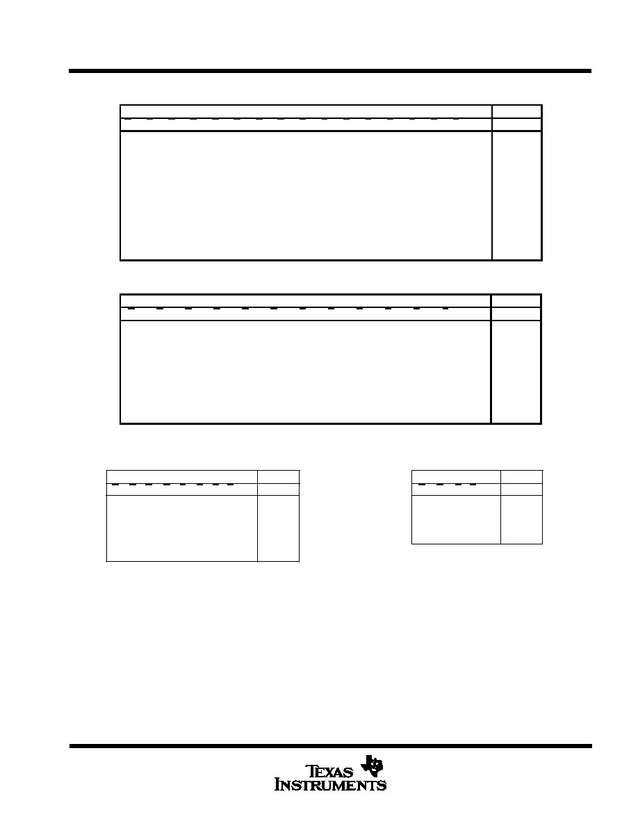
FUNCTION TABLE
FOR Cn + 32 OUTPUT
INPUTS
OUTPUT
G7
G6
G5
G4
G3
G2
G1
G0
P7
P6
P5
P4
P3
P2
P1
P0
Cn
Cn + 32
L
X
X
X
X
X
X
X
X
X
X
X
X
X
X
X
X
H
X
L
X
X
X
X
X
X
L
X
X
X
X
X
X
X
X
H
X
X
L
X
X
X
X
X
L
L
X
X
X
X
X
X
X
H
X
X
X
L
X
X
X
X
L
L
L
X
X
X
X
X
X
H
X
X
X
X
L
X
X
X
L
L
L
L
X
X
X
X
X
H
X
X
X
X
X
L
X
X
L
L
L
L
L
X
X
X
X
H
X
X
X
X
X
X
L
X
L
L
L
L
L
L
X
X
X
H
X
X
X
X
X
X
X
L
L
L
L
L
L
L
L
X
X
H
X
X
X
X
X
X
X
X
L
L
L
L
L
L
L
L
H
H
All other combinations
L
FUNCTION TABLE
FOR Cn+24 OUTPUT
INPUTS
OUTPUT
G5
G4
G3
G2
G1
G0
P5
P4
P3
P2
P1
P0
Cn
Cn + 24
L
X
X
X
X
X
X
X
X
X
X
X
X
H
X
L
X
X
X
X
L
X
X
X
X
X
X
H
X
X
L
X
X
X
L
L
X
X
X
X
X
H
X
X
X
L
X
X
L
L
L
X
X
X
X
H
X
X
X
X
L
X
L
L
L
L
X
X
X
H
X
X
X
X
X
L
L
L
L
L
L
X
X
H
X
X
X
X
X
X
L
L
L
L
L
L
H
H
All other combinations
L
Function Tables
FOR Cn + 8 OUTPUT
FOR Cn + 16 OUTPUT
INPUTS
OUTPUT
X
X
X
L
L
P1 P0 Cn
X
X
X
X
L
X
X
X
X
H
H
H
H
H
H
L
P2
X
X
L
L
L
Cn + 16
P3
X
L
L
L
L
G0
X
X
X
L
X
G1
X
X
L
X
X
G2
X
L
X
X
X
G3
L
X
X
X
X
All other combinations
INPUTS
OUTPUT
H
H
H
L
Cn + 16
Cn
X
X
H
X
L
L
P1 P0
X
X
L
G0
X
L
X
G1
L
X
X
All other combinations
Any inputs not shown in a given table are irrelevant with respect to that output.
SN54AS882A, SN74AS882A
32-BIT LOOK-AHEAD CARRY GENERATORS
SDAS235 ≠ D2661, DECEMBER 1982 ≠ REVISED NOVEMBER 1985
POST OFFICE BOX 655303
∑
DALLAS, TEXAS 75265
4
logic diagram (positive logic)
22
Cn + 32
Cn + 24
17
11
Cn + 16
6
Cn + 8
P7
21
19
P6
16
P5
14
P4
10
P3
8
P2
5
P1
3
P0
20
G7
18
G6
15
G5
13
G4
9
G3
7
G2
4
G1
2
G0
1
Cn
Pin numbers shown are for DW, JT, and NT packages.
SN54AS882A, SN74AS882A
32-BIT LOOK-AHEAD CARRY GENERATORS
SDAS235 ≠ D2661, DECEMBER 1982 ≠ REVISED NOVEMBER 1985
POST OFFICE BOX 655303
∑
DALLAS, TEXAS 75265
5
absolute maximum ratings over operating free-air temperature range (unless otherwise noted)
Supply voltage, V
CC
7 V
. . . . . . . . . . . . . . . . . . . . . . . . . . . . . . . . . . . . . . . . . . . . . . . . . . . . . . . . . . . . . . . . . . . . . . . .
Input voltage
7 V
. . . . . . . . . . . . . . . . . . . . . . . . . . . . . . . . . . . . . . . . . . . . . . . . . . . . . . . . . . . . . . . . . . . . . . . . . . . . . . .
Operating free-air temperature range:
SN54AS882A
≠ 55
∞
C to 125
∞
C
. . . . . . . . . . . . . . . . . . . . . . . . . . . . . .
SN74AS882A
0
∞
C to 70
∞
C
. . . . . . . . . . . . . . . . . . . . . . . . . . . . . . . . . .
Storage temperature range
≠ 65
∞
C to 150
∞
C
. . . . . . . . . . . . . . . . . . . . . . . . . . . . . . . . . . . . . . . . . . . . . . . . . . . . . . .
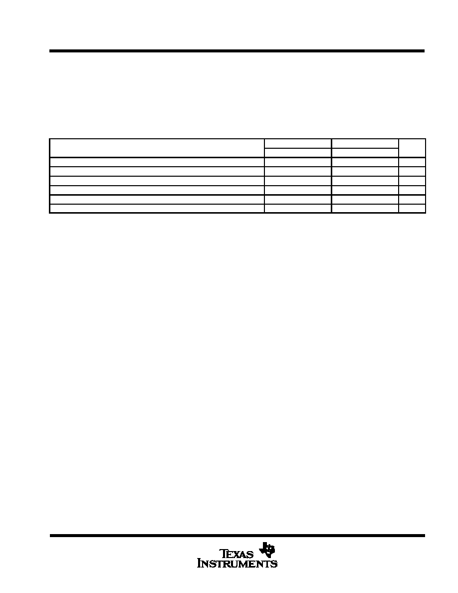
recommended operating conditions
SN54AS882A
SN74AS882A
UNIT
MIN
NOM
MAX
MIN
NOM
MAX
UNIT
VCC
Supply voltage
4.5
5
5.5
4.5
5
5.5
V
VIH
High-level input voltage
2
2
V
VIL
Low-level input voltage
0.8
0.8
V
IOH
High-level output current
≠ 2
≠ 2
mA
IOL
Low-level output current
20
20
mA
TA
Operating free-air temperature
≠ 55
125
0
70
∞
C
SN54AS882A, SN74AS882A
32-BIT LOOK-AHEAD CARRY GENERATORS
SDAS235 ≠ D2661, DECEMBER 1982 ≠ REVISED NOVEMBER 1985
POST OFFICE BOX 655303
∑
DALLAS, TEXAS 75265
6
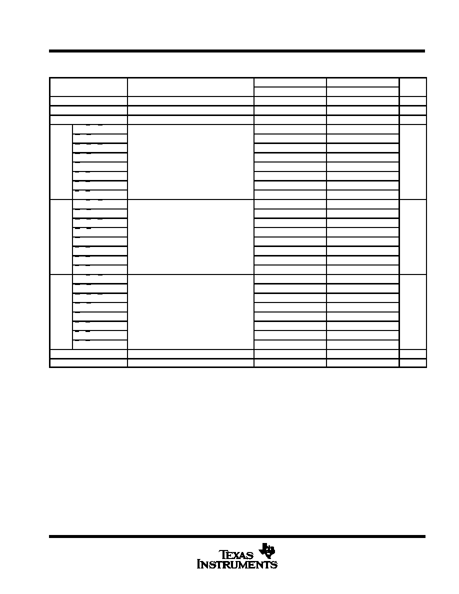
electrical characteristics over recommended operating free-air temperature range (unless
otherwise noted)
PARAMETER
TEST CONDITIONS
SN54AS882A
SN74AS882A
UNIT
PARAMETER
TEST CONDITIONS
MIN
TYP
MAX
MIN
TYP
MAX
UNIT
VIK
VCC = 4.5 V,
II = ≠ 18 mA
≠ 1.2
≠ 1.2
V
VOH
VCC = 4.5 V to 5.5 V,
IOH = ≠ 2 mA
VCC ≠ 2
VCC ≠ 2
V
VOL
VCC = 4.5 V,
IOL = 20 mA
0.3
0.5
0.3
0.5
V
Cn, P 0, P1
0.4
0.4
G0, G6
0.8
0.8
G1, G2, G4
1.2
1.2
II
G3, G5
VCC = 5.5 V,
VI = 7 V
1.5
1.5
mA
G7
0.9
0.9
P2, P3
0.3
0.3
P4, P5
0.2
0.2
P6, P7
0.1
0.1
Cn, P 0, P1
80
80
G0, G6
160
160
G1, G2, G4
240
240
IIH
G3, G5
VCC = 5.5 V,
VI = 2.7 V
300
300
µ
A
G7
180
180
P2, P3
60
60
P4, P5
40
40
P6, P7
20
20
Cn, P 0, P1
≠ 2
≠ 2
G0, G6
≠ 4
≠ 4
G1, G2, G4
≠ 6
≠ 6
IIL
G3, G5
VCC = 5.5 V,
VI = 0.4 V
≠ 7.5
≠ 7.5
mA
G7
≠ 4.5
≠ 4.5
P2, P3
≠ 1.5
≠ 1.5
P4, P5
≠ 1
≠ 1
P6, P7
≠ 0.5
≠ 0.5
IO
VCC = 5.5 V,
VO = 2.25 V
≠ 30
≠ 130
≠ 30
≠ 30
mA
ICC
VCC = 5.5 V
44
70
44
70
mA
All typical values are at VCC = 5 V, TA = 25
∞
C.
The output conditions have been chosen to produce a current that closely approximates one half of the true short-circuit output current, IOS.
SN54AS882A, SN74AS882A
32-BIT LOOK-AHEAD CARRY GENERATORS
SDAS235 ≠ D2661, DECEMBER 1982 ≠ REVISED NOVEMBER 1985
POST OFFICE BOX 655303
∑
DALLAS, TEXAS 75265
7
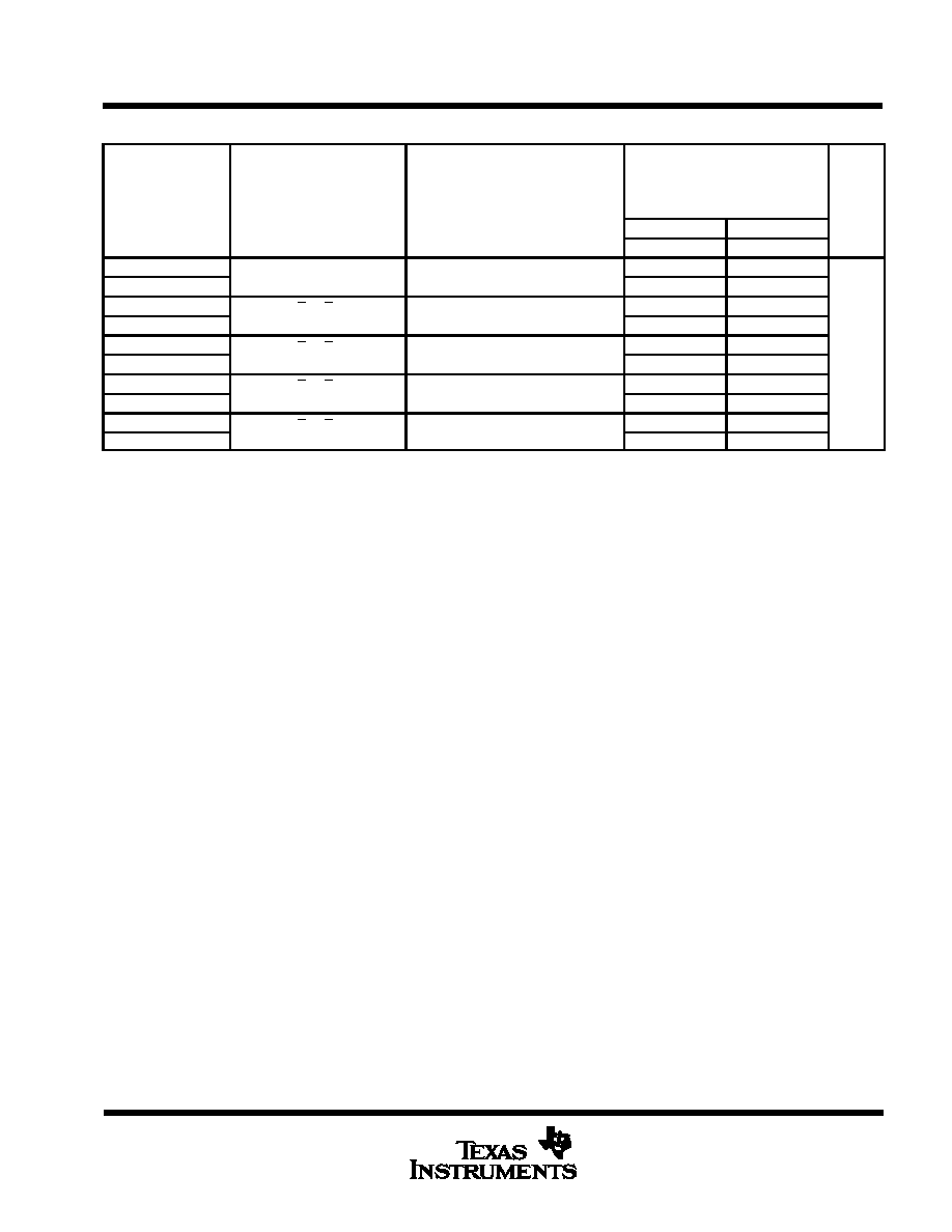
switching characteristics (see Note 1)
VCC = 4.5 V to 5.5 V,
CL = 50 pF
CL = 50 pF,
RL = 500
PARAMETER
FROM
TO
RL = 500
,
T
MIN t MAX
UNIT
PARAMETER
FROM
(INPUT)
TO
(OUTPUT)
TA = MIN to MAX
UNIT
(INPUT)
(OUTPUT)
SN54AS882A
SN74AS882A
MIN
MAX
MIN
MAX
tPLH
C
Any output
2
10
2
9
tPHL
Cn
Any output
3
15
3
14
tPLH
P or G
C + 8
2
8
2
7
tPHL
P or G
Cn + 8
2
8
2
7
tPLH
P or G
C + 16
2
8
2
7
ns
tPHL
P or G
Cn + 16
2
8
2
7
tPLH
P or G
C + 24
2
8
2
7
tPHL
P or G
Cn + 24
2
11
2
10
tPLH
P or G
Cn + 32
1.5
9
2
8
tPHL
P or G
Cn + 32
2
13
2
12
NOTE 1: Load circuits and voltage waveforms are shown in Section 1.
SN54AS882A, SN74AS882A
32-BIT LOOK-AHEAD CARRY GENERATORS
SDAS235 ≠ D2661, DECEMBER 1982 ≠ REVISED NOVEMBER 1985
POST OFFICE BOX 655303
∑
DALLAS, TEXAS 75265
8
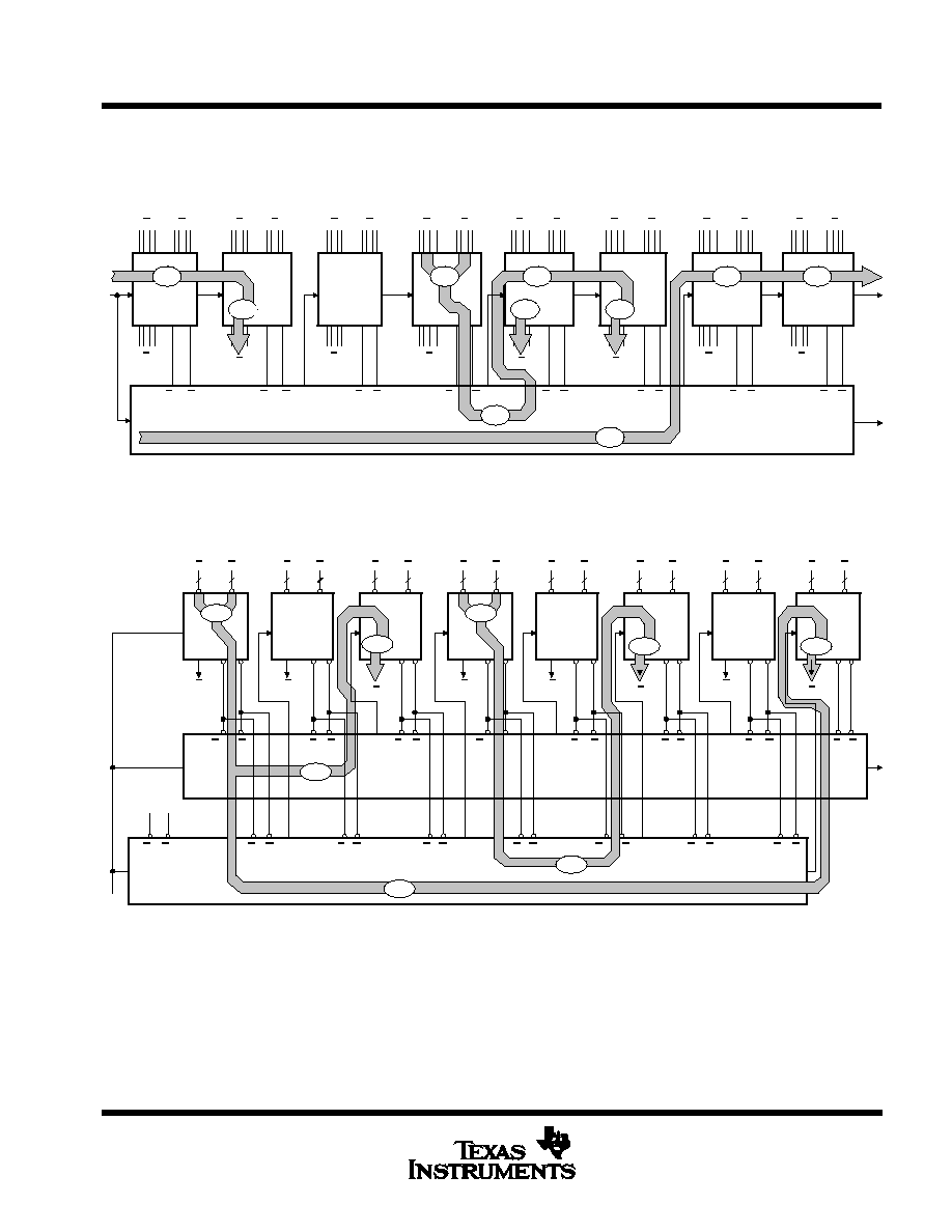
TYPICAL APPLICATION DATA
The application given in Figure 1 illustrates how the 'AS882A can implement look-ahead carry for a 32-bit ALU
(in this case, the popular 'AS881A) with a single package. Typical carry times shown are derived using the
standard Advanced Schottky load circuit.
'AS881A
'AS881A
'AS881A
Cn+16
Cn + 8
'AS881A
6 ns
6 ns
A
B
Cn
Cn≠4
'AS881A
Cn≠4
Cn
Cn
B
A
B
A
F
F
F
'AS881A
Cn
F
A
B
6 ns
F
Cn≠4
Cn≠4
Cn≠4
P0
G0
G1
P1
G2
P2
P4 G4
P3
G3
F
F
B
A
B
A
B
A
B
A
F
G5
P5
G6
P6
G7
P7
Cn + 24
7 ns
MSB
LSB
Cn
'AS882A
Cn + 32
Cn
Cn
Cn
Cn
Cn≠4
Cn≠4
Cn≠4
'AS881A
'AS881A
6 ns
6 ns
6 ns
6 ns
6 ns
6 ns
Figure 1
Likewise, Figure 2 illustrates the same 32-bit ALU using two 'AS882s. This shows the worst-case delay from
LSB to MSB to be 19 ns as opposed to 25 ns in Figure 1.
Cn
6 ns
7 ns
F
F
A
4
4
B
4
A
4
B
4
A
LSB
B
4
Cn
L
P0 G0
H
G1
P1
G2
P2
Cn
Cn
Cn + 8
4
B
A
4
B
4
4
A
F
Cn
6 ns
4
A
B
4
F
F
'AS881A
'AS881A
'AS881A
'AS881A
'AS881A
'AS881A
'AS881A
'AS881A
Cn
Cn
Cn
Cn
F
F
F
A
B
4
A
4
B
Cn + 16
Cn + 24
Cn + 32
P3 G3
P4 G4
P6 G6
P7 G7
G5
P5
'AS882A
P0
G0
P1 G1
Cn + 16
P2
Cn
G2
P3
G3
P4 G4
'AS882A
P5 G5
G6
P6
Cn + 24
P7 G7
Cn + 32
MSB
6 ns
6 ns
6 ns
6 ns
6 ns
Figure 2

IMPORTANT NOTICE
Texas Instruments and its subsidiaries (TI) reserve the right to make changes to their products or to discontinue
any product or service without notice, and advise customers to obtain the latest version of relevant information
to verify, before placing orders, that information being relied on is current and complete. All products are sold
subject to the terms and conditions of sale supplied at the time of order acknowledgement, including those
pertaining to warranty, patent infringement, and limitation of liability.
TI warrants performance of its semiconductor products to the specifications applicable at the time of sale in
accordance with TI's standard warranty. Testing and other quality control techniques are utilized to the extent
TI deems necessary to support this warranty. Specific testing of all parameters of each device is not necessarily
performed, except those mandated by government requirements.
CERTAIN APPLICATIONS USING SEMICONDUCTOR PRODUCTS MAY INVOLVE POTENTIAL RISKS OF
DEATH, PERSONAL INJURY, OR SEVERE PROPERTY OR ENVIRONMENTAL DAMAGE ("CRITICAL
APPLICATIONS"). TI SEMICONDUCTOR PRODUCTS ARE NOT DESIGNED, AUTHORIZED, OR
WARRANTED TO BE SUITABLE FOR USE IN LIFE-SUPPORT DEVICES OR SYSTEMS OR OTHER
CRITICAL APPLICATIONS. INCLUSION OF TI PRODUCTS IN SUCH APPLICATIONS IS UNDERSTOOD TO
BE FULLY AT THE CUSTOMER'S RISK.
In order to minimize risks associated with the customer's applications, adequate design and operating
safeguards must be provided by the customer to minimize inherent or procedural hazards.
TI assumes no liability for applications assistance or customer product design. TI does not warrant or represent
that any license, either express or implied, is granted under any patent right, copyright, mask work right, or other
intellectual property right of TI covering or relating to any combination, machine, or process in which such
semiconductor products or services might be or are used. TI's publication of information regarding any third
party's products or services does not constitute TI's approval, warranty or endorsement thereof.
Copyright
©
1998, Texas Instruments Incorporated