SN75185
MULTIPLE RS 232 DRIVERS AND RECEIVERS
SLLS181C - DECEMBER 1994 - REVISED OCTOBER 2003
1
POST OFFICE BOX 655303
∑
DALLAS, TEXAS 75265
D
Single Chip With Easy Interface Between
UART and Serial-Port Connector of IBM
PC/AT
and Compatibles
D
Meets or Exceeds the Requirements of
TIA/EIA-232-F and ITU v.28 Standards
D
Supports Data Rates Up To 120 kbit/s
D
ESD Protection Meets or Exceeds 10 kV on
RS-232 Pins and 3.5 kV on All Other Pins
(Human-Body Model)
D
Pin-to-Pin Compatible With the SN75C185
description/ordering information
The SN75185 combines three drivers and five receivers from the TI SN75188 and SN75189 bipolar quadruple
drivers and receivers, respectively. The pinout matches the flow-through design of the SN75C185 to decrease
the part count, reduce the board space required, and allow easy interconnection of the UART and serial-port
connector of IBM
PC/AT
and compatibles. The bipolar circuits and processing of the SN75185 provide a
rugged low-cost solution for this function at the expense of quiescent power and external passive components
relative to the SN75C185.
The SN75185 complies with the requirements of the TIA/EIA-232-F and ITU v.28 standards. These standards
are for data interchange between a host computer and peripheral at signaling rates up to 20 kbit/s. The switching
speeds of the SN75185 are fast enough to support rates up to 120 kbit/s with lower capacitive loads (shorter
cables). Interoperability at the higher signaling rates cannot be assured unless the designer has design control
of the cable and the interface circuits at both ends. For interoperability at signaling rates to 120 kbit/s, use of
TIA/EIA-423-B (ITU v.10) and TIA/EIA-422-B (ITU v.11) standards is recommended.
The SN75185 is characterized for operation over the temperature range of 0
∞
C to 70
∞
C.
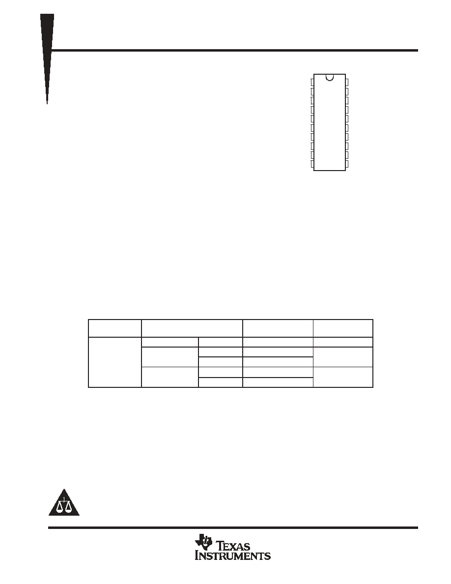
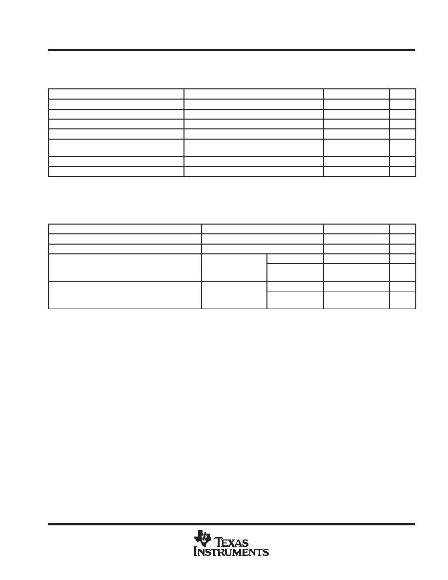
ORDERING INFORMATION
TA
PACKAGE
ORDERABLE
PART NUMBER
TOP-SIDE
MARKING
PDIP (N)
Tube of 20
SN75185N
SN75185N
SOIC (DW)
Tube of 25
SN75185DW
SN75185
0
∞
C to 70
∞
C
SOIC (DW)
Reel of 2000
SN75185DWR
SN75185
0 C to 70 C
SSOP (DB)
Tube of 70
SN75185DB
A185
SSOP (DB)
Reel of 2000
SN75185DBR
A185
Package drawings, standard packing quantities, thermal data, symbolization, and PCB design guidelines are
available at www.ti.com/sc/package.
Copyright
2003, Texas Instruments Incorporated
PRODUCTION DATA information is current as of publication date.
Products conform to specifications per the terms of Texas Instruments
standard warranty. Production processing does not necessarily include
testing of all parameters.
Please be aware that an important notice concerning availability, standard warranty, and use in critical applications of
Texas Instruments semiconductor products and disclaimers thereto appears at the end of this data sheet.
1
2
3
4
5
6
7
8
9
10
20
19
18
17
16
15
14
13
12
11
V
DD
RA1
RA2
RA3
DY1
DY2
RA4
DY3
RA5
V
SS
V
CC
RY1
RY2
RY3
DA1
DA2
RY4
DA3
RY5
GND
DB, DW, OR N PACKAGE
(TOP VIEW)
IBM and PC/AT are trademarks of IBM Corporation.
SN75185
MULTIPLE RS 232 DRIVERS AND RECEIVERS
SLLS181C - DECEMBER 1994 - REVISED OCTOBER 2003
2
POST OFFICE BOX 655303
∑
DALLAS, TEXAS 75265
logic diagram (positive logic)
RA1
RY1
2
19
RA2
RY2
3
18
RA3
RY3
4
17
DY1
DA1
5
16
DY2
DA2
6
15
RA4
RY4
7
14
DY3
DA3
8
13
RA5
RY5
9
12
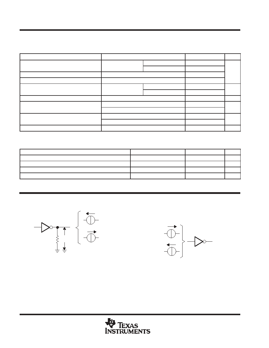
schematic of drivers
DYx
Output
320
68.5
3.3 k
10.4 k
To Other Drivers
VSS
To Other
Drivers
GND
4.2 k
DAx
Input
VDD
75.8
9.4 k
11.6 k
To Other Drivers
Resistor values shown are nominal.
ESD
ESD
ESD
ESD
SN75185
MULTIPLE RS 232 DRIVERS AND RECEIVERS
SLLS181C - DECEMBER 1994 - REVISED OCTOBER 2003
3
POST OFFICE BOX 655303
∑
DALLAS, TEXAS 75265
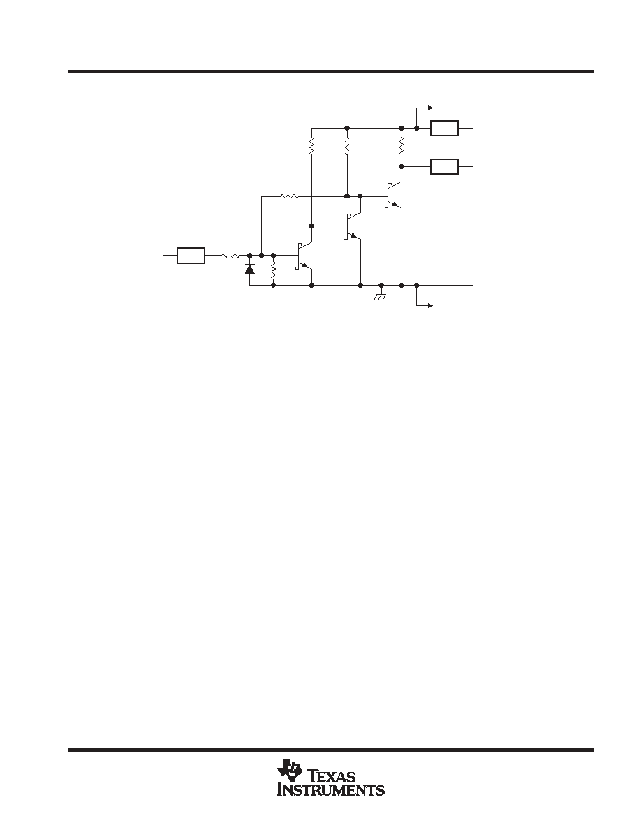
schematic (each receiver)
RAx
Input
10 k
3.8 k
9 k
5 k
1.66 k
GND
RYx
Output
VCC
ESD
To Other Receivers
Resistor values shown are nominal.
2 k
ESD
To Other Receivers
ESD
absolute maximum ratings over operating free-air temperature range (unless otherwise noted)
Supply voltage (see Note 1): V
CC
10
V
. . . . . . . . . . . . . . . . . . . . . . . . . . . . . . . . . . . . . . . . . . . . . . . . . . . . . . . . . . .
V
DD
15
V
. . . . . . . . . . . . . . . . . . . . . . . . . . . . . . . . . . . . . . . . . . . . . . . . . . . . . . . . . . .
V
SS
-15
V
. . . . . . . . . . . . . . . . . . . . . . . . . . . . . . . . . . . . . . . . . . . . . . . . . . . . . . . . . . .
Input voltage range: Driver
-15 V to 7 V
. . . . . . . . . . . . . . . . . . . . . . . . . . . . . . . . . . . . . . . . . . . . . . . . . . . . . . . . . . .
Receiver
-30 V to 30 V
. . . . . . . . . . . . . . . . . . . . . . . . . . . . . . . . . . . . . . . . . . . . . . . . . . . . . . .
Driver output voltage range
-15 V to 15 V
. . . . . . . . . . . . . . . . . . . . . . . . . . . . . . . . . . . . . . . . . . . . . . . . . . . . . . . . .
Receiver low-level output current
20 mA
. . . . . . . . . . . . . . . . . . . . . . . . . . . . . . . . . . . . . . . . . . . . . . . . . . . . . . . . . .
Package thermal impedance,
JA
(see Notes 2 and 3): DB package
70
∞
C/W
. . . . . . . . . . . . . . . . . . . . . . . . . . .
DW package
58
∞
C/W
. . . . . . . . . . . . . . . . . . . . . . . . . .
N package
69
∞
C/W
. . . . . . . . . . . . . . . . . . . . . . . . . . . .
Operating virtual junction temperature, T
J
150
∞
C
. . . . . . . . . . . . . . . . . . . . . . . . . . . . . . . . . . . . . . . . . . . . . . . . . . .
Electrostatic discharge: Human-Body Model: RS-232 pins, class 3, A (see Note 4)
10 kV
. . . . . . . . . . . . . . . .
All pins, class 3, A (see Note 5)
3.5 kV
. . . . . . . . . . . . . . . . . . . .
Machine Model: RS-232 pins, class 3, B (see Note 6)
600 V
. . . . . . . . . . . . . . . . . . . .
All pins, class 3, B (see Note 4)
250 V
. . . . . . . . . . . . . . . . . . . . . . . .
Storage temperature range, T
stg
-65
∞
C to 150
∞
C
. . . . . . . . . . . . . . . . . . . . . . . . . . . . . . . . . . . . . . . . . . . . . . . . . . .
Stresses beyond those listed under "absolute maximum ratings" may cause permanent damage to the device. These are stress ratings only, and
functional operation of the device at these or any other conditions beyond those indicated under "recommended operating conditions" is not
implied. Exposure to absolute-maximum-rated conditions for extended periods may affect device reliability.
NOTES:
1. All voltages are with respect to the network ground terminal.
2. Maximum power dissipation is a function of TJ(max),
JA, and TA. The maximum allowable power dissipation at any allowable
ambient temperature is PD = (TJ(max) - TA)/
JA. Operating at the absolute maximum TJ of 150
∞
C can affect reliability.
3. The package thermal impedance is calculated in accordance with JESD 51-7.
4. RS-232 pins are tested with respect to ground and to each other.
5. Per MIL-PRF-38535
6. RS-232 pins are tested with respect to ground.
SN75185
MULTIPLE RS 232 DRIVERS AND RECEIVERS
SLLS181C - DECEMBER 1994 - REVISED OCTOBER 2003
4
POST OFFICE BOX 655303
∑
DALLAS, TEXAS 75265
recommended operating conditions
MIN
NOM
MAX
UNIT
VCC
Supply voltage
4.5
5
5.5
V
VDD
Supply voltage
7.5
9
15
V
VSS
Supply voltage
-7.5
-9
-15
V
VIH
High-level input voltage (drivers only)
1.9
V
VIL
Low-level input voltage (drivers only)
0.8
V
IOH
High-level output current
Drivers
-6
mA
IOH
High-level output current
Receivers
-0.5
mA
IOL
Low-level output current
Drivers
6
mA
IOL
Low-level output current
Receivers
16
mA
TA
Operating free-air temperature
0
70
∞
C
supply currents
PARAMETER
TEST CONDITIONS
MIN
MAX
UNIT
ICC
Supply current from VCC
All inputs at 5 V,
No load,
VCC = 5 V
30
mA
VDD = 9 V,
VSS = -9 V
15
All inputs at 1.9 V,
No load
VDD = 12 V,
VSS = -12 V
19
IDD
Supply current from VDD
All inputs at 1.9 V,
No load
VDD = 15 V,
VSS = -15 V
25
mA
IDD
Supply current from VDD
VDD = 9 V,
VSS = -9 V
4.5
mA
All inputs at 0.8 V,
No load
VDD = 12 V,
VSS = -12 V
5.5
All inputs at 0.8 V,
No load
VDD = 15 V,
VSS = -15 V
9
VDD = 9 V,
VSS = -9 V
-15
All inputs at 1.9 V,
No load
VDD = 12 V,
VSS = -12 V
-19
ISS
Supply current from VSS
All inputs at 1.9 V,
No load
VDD = 15 V,
VSS = -15 V
-25
mA
ISS
Supply current from VSS
VDD = 9 V,
VSS = -9 V
-3.2
mA
All inputs at 0.8 V,
No load
VDD = 12 V,
VSS = -12 V
-3.2
All inputs at 0.8 V,
No load
VDD = 15 V,
VSS = -15 V
-3.2
SN75185
MULTIPLE RS 232 DRIVERS AND RECEIVERS
SLLS181C - DECEMBER 1994 - REVISED OCTOBER 2003
5
POST OFFICE BOX 655303
∑
DALLAS, TEXAS 75265
DRIVER SECTION
electrical characteristics over recommended operating free-air temperature range, V
DD
= 9 V,
V
SS
= -9 V, V
CC
= 5 V (unless otherwise noted)
PARAMETER
TEST CONDITIONS
MIN
TYP
MAX
UNIT
VOH
High-level output voltage
VIL = 0.8 V,
RL = 3 k
,
See Figure 1
6
7.5
V
VOL
Low-level output voltage (see Note 7)
VIH = 1.9 V,
RL = 3 k
,
See Figure 1
-7.5
-6
V
IIH
High-level input current
VI = 5 V,
See Figure 2
10
µ
A
IIL
Low-level input current
VI = 0,
See Figure 2
-1.6
mA
IOS(H)
High-level short-circuit output current
(see Note 8)
VIL = 0.8 V,
VO = 0,
See Figure 1
-4.5
-12
-19.5
mA
IOS(L)
Low-level short-circuit output current
VIH = 2 V,
VO = 0,
See Figure 1
4.5
12
19.5
mA
ro
Output resistance (see Note 9)
VCC = VDD = VSS = 0,
VO = -2 V to 2 V
300
NOTES:
7. The algebraic convention, in which the more positive (less negative) limit is designated as maximum, is used in this data sheet for
logic levels only (e.g., if -10 V is maximum, the typical value is a more negative voltage).
8. Output short-circuit conditions must maintain the total power dissipation below absolute maximum ratings.
9. Test conditions are those specified by TIA/EIA-232-F and as listed above.
switching characteristics, V
CC
= 5 V, V
DD
= 12 V, V
SS
= -12 V, T
A
= 25
∞
C (see Figure 3)
PARAMETER
TEST CONDITIONS
MIN
TYP
MAX
UNIT
tPLH Propagation delay time, low- to high-level output
RL = 3 k
to 7 k
,
CL = 15 pF
315
500
ns
tPHL Propagation delay time, high- to low-level output
RL = 3 k
to 7 k
,
CL = 15 pF
75
175
ns
CL = 15 pF
60
100
ns
tTLH
Transition time, low- to high-level output
RL = 3 k
to 7 k
CL = 2500 pF,
See Note 10
1.7
2.5
µ
s
CL = 15 pF
40
75
ns
tTHL
Transition time, high- to low-level output
RL = 3 k
to 7 k
CL = 2500 pF,
See Note 11
1.5
2.5
µ
s
NOTES: 10. Measured between -3-V and 3-V points of the output waveform (TIA/EIA-232-F conditions); all unused inputs are tied either high
or low.
11. Measured between 3-V and -3-V points of the output waveform (TIA/EIA-232-F conditions); all unused inputs are tied either high
or low.
SN75185
MULTIPLE RS 232 DRIVERS AND RECEIVERS
SLLS181C - DECEMBER 1994 - REVISED OCTOBER 2003
6
POST OFFICE BOX 655303
∑
DALLAS, TEXAS 75265
RECEIVER SECTION
electrical characteristics over recommended operating conditions (unless otherwise noted)
PARAMETER
TEST CONDITIONS
MIN
TYP
MAX
UNIT
VT+
Positive-going threshold voltage
See Figure 5
TA = 25
∞
C
1.75
1.9
2.3
VT+
Positive-going threshold voltage
See Figure 5
TA = 0
∞
C to 70
∞
C
1.55
2.3
V
VT-
Negative-going threshold voltage
0.75
0.97
1.25
V
Vhys Input hysteresis (VT+ - VT-)
0.5
VOH
High-level output voltage
IOH = -0.5 mA
VIH = 0.75 V
2.6
4
5
V
VOH
High-level output voltage
IOH = -0.5 mA
Inputs open
2.6
V
VOL
Low-level input voltage
IOL = 10 mA,
VI = 3 V
0.2
0.45
V
IIH
High-level input current
VI = 25 V,
See Figure 5
3.6
8.3
mA
IIH
High-level input current
VI = 3 V,
See Figure 5
0.43
mA
IIL
Low-level output current
VI = -25 V,
See Figure 5
-3.6
-8.3
mA
IIL
Low-level output current
VI = -3 V,
See Figure 5
-0.43
mA
IOS
Short-circuit output current
See Figure 4
-3.4
-12
mA
All typical values are at TA = 25
∞
C, VCC = 5 V, VDD = 9 V, and VSS = -9 V.
switching characteristics, V
CC
= 5 V, V
DD
= 12 V, V
SS
= -12 V, T
A
= 25
∞
C (see Figure 6)
PARAMETER
TEST CONDITIONS
MIN
TYP
MAX
UNIT
tPLH
Propagation delay time, low- to high-level output
CL = 50 pF,
RL = 5 k
107
500
ns
tPHL
Propagation delay time, high- to low-level output
CL = 50 pF,
RL = 5 k
42
150
ns
tTLH
Transition time, low- to high-level output
CL = 50 pF,
RL = 5 k
175
525
ns
tTHL
Transition time, high- to low-level output
CL = 50 pF,
RL = 5 k
16
60
ns
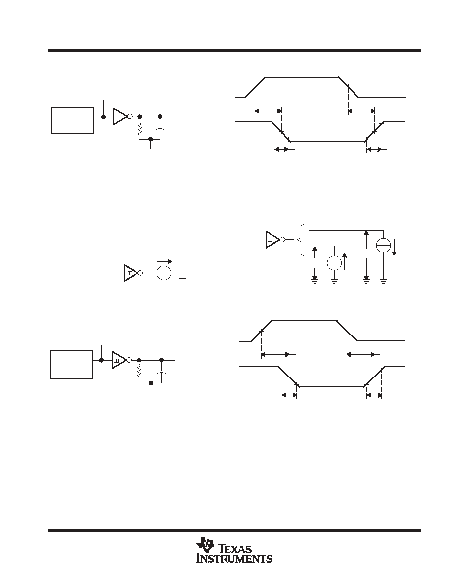
PARAMETER MEASUREMENT INFORMATION
Figure 1. Driver Test Circuit for
V
OH
, V
OL
, I
OS(H)
, and I
OS(L)
IOS(L)
-IOS(H)
VI
VO
VDD or GND
VSS or GND
RL = 3 k
Figure 2. Driver Test Circuit for I
IH
and I
IL
-IIL
IIH
VI
VI
SN75185
MULTIPLE RS 232 DRIVERS AND RECEIVERS
SLLS181C - DECEMBER 1994 - REVISED OCTOBER 2003
7
POST OFFICE BOX 655303
∑
DALLAS, TEXAS 75265
PARAMETER MEASUREMENT INFORMATION
Pulse
Generator
(see Note B)
CL
(see Note A)
RL
3 V
0 V
1.5 V
1.5 V
Input
tPHL
tPLH
90%
50%
10%
50%
10%
90%
tTHL
tTLH
VOH
VOL
TEST CIRCUIT
VOLTAGE WAVEFORMS
Input
Output
NOTES: A. CL includes probe and jig capacitance.
B. The pulse generator has the following characteristics: tw = 25
µ
s, PRR = 20 kHz, ZO = 50
, tr = tf < 50 ns.
Output
Figure 3. Driver Test Circuit and Voltage Waveforms
Figure 4. Receiver Test Circuit for I
OS
VI
Figure 5. Receiver Test Circuit for V
T
, V
OH
, and V
OL
VT,
VI
IOL
VOH
-IOH
VOL
Pulse
Generator
(see Note B)
CL
(see Note A)
RL
4 V
0 V
50%
50%
Input
tPHL
tPLH
90%
50%
10%
50%
10%
90%
tTHL
tTLH
VOH
VOL
TEST CIRCUIT
VOLTAGE WAVEFORMS
Input
Output
NOTES: A. CL includes probe and jig capacitance.
B. The pulse generator has the following characteristics: tw = 25
µ
s, PRR = 20 kHz, ZO = 50
, tr = tf < 50 ns.
Output
Figure 6. Receiver Propagation and Transition Times
SN75185
MULTIPLE RS 232 DRIVERS AND RECEIVERS
SLLS181C - DECEMBER 1994 - REVISED OCTOBER 2003
8
POST OFFICE BOX 655303
∑
DALLAS, TEXAS 75265
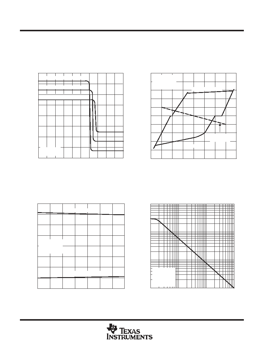
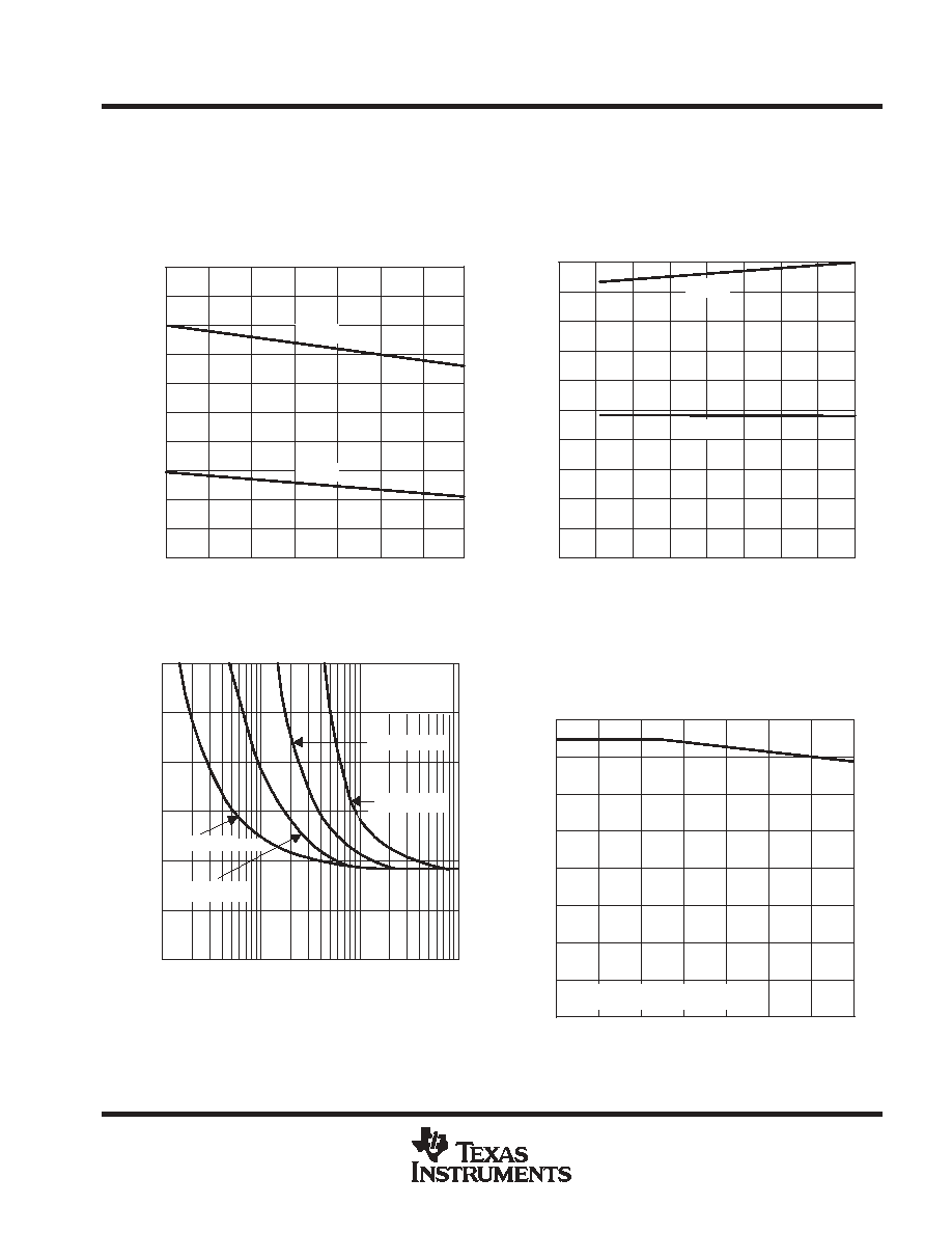
TYPICAL CHARACTERISTICS
DRIVER SECTION
Figure 7
VOLTAGE TRANSFER CHARACTERISTICS
VDD = 6 V, VSS = -6 V
VI - Input Voltage - V
VDD = 12 V, VSS = -12 V
VDD = 9 V, VSS = -9 V
RL = 3 k
TA = 25
∞
C
12
9
6
3
0
-3
-6
-9
-12
0
0.2
0.4
0.6
0.8
1
1.2
1.4
1.6
1.8
2
V
-
Output V
oltage - V
O
Figure 8
OUTPUT CURRENT
vs
OUTPUT VOLTAGE
VOH (VI = 0.8 V)
VO - Output Voltage - V
3-k
Load Line
VDD = 9 V
VSS = -9 V
TA = 25
∞
C
I
-
Output Current - mA
O
VOL (VI = 1.9 V)
8
4
0
-4
-8
-12
-16
-20
12
16
20
-16
-12
-8
-4
0
4
8
12
16
Figure 9
SHORT-CIRCUIT OUTPUT CURRENT
vs
FREE-AIR TEMPERATURE
TA - Free-Air Temperature -
∞
C
IOS(H) (VI = 0.8 V)
IOS(L) (VI = 1.9 V)
VDD = 9 V
VSS = -9 V
VO = 0
12
9
6
3
0
-3
-6
-9
0
10
20
30
40
50
60
70
-12
I
-
Short-Circuit Output Current - mA
OS
Figure 10
SLEW RATE
vs
LOAD CAPACITANCE
CL - Load Capacitance - pF
SR - Slew Rate - V/
µ
s
VDD = 9 V
VSS = -9 V
RL = 3 k
TA = 25
∞
C
1000
100
10
1
10
100
1000
10000
SN75185
MULTIPLE RS 232 DRIVERS AND RECEIVERS
SLLS181C - DECEMBER 1994 - REVISED OCTOBER 2003
9
POST OFFICE BOX 655303
∑
DALLAS, TEXAS 75265
TYPICAL CHARACTERISTICS
RECEIVER SECTION
Figure 11
Input Threshold V
o
ltage - V
INPUT THRESHOLD VOLTAGE
vs
FREE-AIR TEMPERATURE
TA - Free-Air Temperature -
∞
C
VT-
VT+
2.4
2.2
2
1.8
1.6
1.4
1.2
1
0.8
0.6
0.4
0
10
20
30
40
50
60
70
Figure 12
INPUT THRESHOLD VOLTAGE
vs
SUPPLY VOLTAGE
VCC - Supply Voltage - V
Input Threshold V
o
ltage - V
VT-
VT+
2
1.8
1.6
1.4
1.2
1
0.8
0.6
0.4
2
3
4
5
6
7
8
9
10
0
0.2
Figure 13
Amplitude - V
NOISE REJECTION
CC = 300 pF
VCC = 5 V
TA = 25
∞
C
See Note A
tw - Pulse Duration - ns
CC = 500 pF
CC = 12 pF
CC = 100 pF
NOTE
A: This figure shows the maximum amplitude of a
positive-going pulse that, starting from 0 V, will not cause a
change in the output level.
6
5
4
3
2
1
0
10
40
100
400
1000
4000 10000
Figure 14
MAXIMUM SUPPLY VOLTAGE
vs
FREE-AIR TEMPERATURE
TA - Free-Air Temperature -
∞
C
RL
3 k
(from each output to GND)
V
-
Supply V
o
ltage - V
CC
16
14
12
10
8
6
4
2
0
0
10
20
30
40
50
60
70
SN75185
MULTIPLE RS 232 DRIVERS AND RECEIVERS
SLLS181C - DECEMBER 1994 - REVISED OCTOBER 2003
10
POST OFFICE BOX 655303
∑
DALLAS, TEXAS 75265
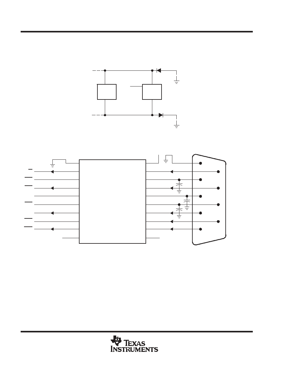
APPLICATION INFORMATION
Diodes placed in series with the V
DD
and V
SS
leads protect the SN75185 in the fault condition. In the fault condition,
the device outputs are shorted to
±
15 V, and the power supplies are at low and provide low-impedance paths to ground
(see Figure 15).
VDD
VSS
±
15 V
Output
VDD
VSS
SN75185
SN75185
Figure 15. Power-Supply Protection to Meet Power-Off Fault Conditions of TIA/EIA-232-F
11
12
13
14
15
16
17
18
19
20
GND
RY5
DA3
RY4
DA2
DA1
RY3
RY2
RY1
VCC
VSS
RA5
DY3
RA4
DY2
DY1
RA3
RA2
RA1
VDD
10
9
8
7
6
5
4
3
2
1
43
37
40
13
36
11
41
42
RI
DTR
CTS
SO
RTS
SI
DSR
DCD
R1
DTR
CTS
TX
RTS
RX
DSR
DCD
SN75185
5 V
TL16C450
ACE
1
5
6
9
12 V
-12 V
TIA/EIA-232-F
DB9S
Connector
C1
C3
See Figure 10 to select the correct values for the loading capacitors (C1, C2, and C3), which are required to meet the RS-232 maximum
slew-rate requirement of 30 V/
µ
s. The value of the loading capacitors required depends on the line length and desired slew rate, but typically
is 330 pF.
C2
Figure 16. Typical Connection
MECHANICAL
MPDI002C ≠ JANUARY 1995 ≠ REVISED DECEMBER 20002
POST OFFICE BOX 655303
∑
DALLAS, TEXAS 75265
N (R-PDIP-T**)
PLASTIC DUAL-IN-LINE PACKAGE
BB
AC
AD
0.325 (8,26)
0.300 (7,62)
0.010 (0,25) NOM
Gauge Plane
0.015 (0,38)
0.430 (10,92) MAX
20
1.060
(26,92)
0.940
(23,88)
18
0.920
0.850
14
0.775
0.745
(19,69)
(18,92)
16
0.775
(19,69)
(18,92)
0.745
A MIN
DIM
A MAX
PINS **
(23,37)
(21,59)
Seating Plane
14/18 PIN ONLY
20 pin vendor option
4040049/E 12/2002
9
8
0.070 (1,78)
A
0.045 (1,14)
0.020 (0,51) MIN
16
1
0.015 (0,38)
0.021 (0,53)
0.200 (5,08) MAX
0.125 (3,18) MIN
0.240 (6,10)
0.260 (6,60)
M
0.010 (0,25)
0.100 (2,54)
16 PINS SHOWN
MS-100
VARIATION
AA
C
D
D
D
0.030 (0,76)
0.045 (1,14)
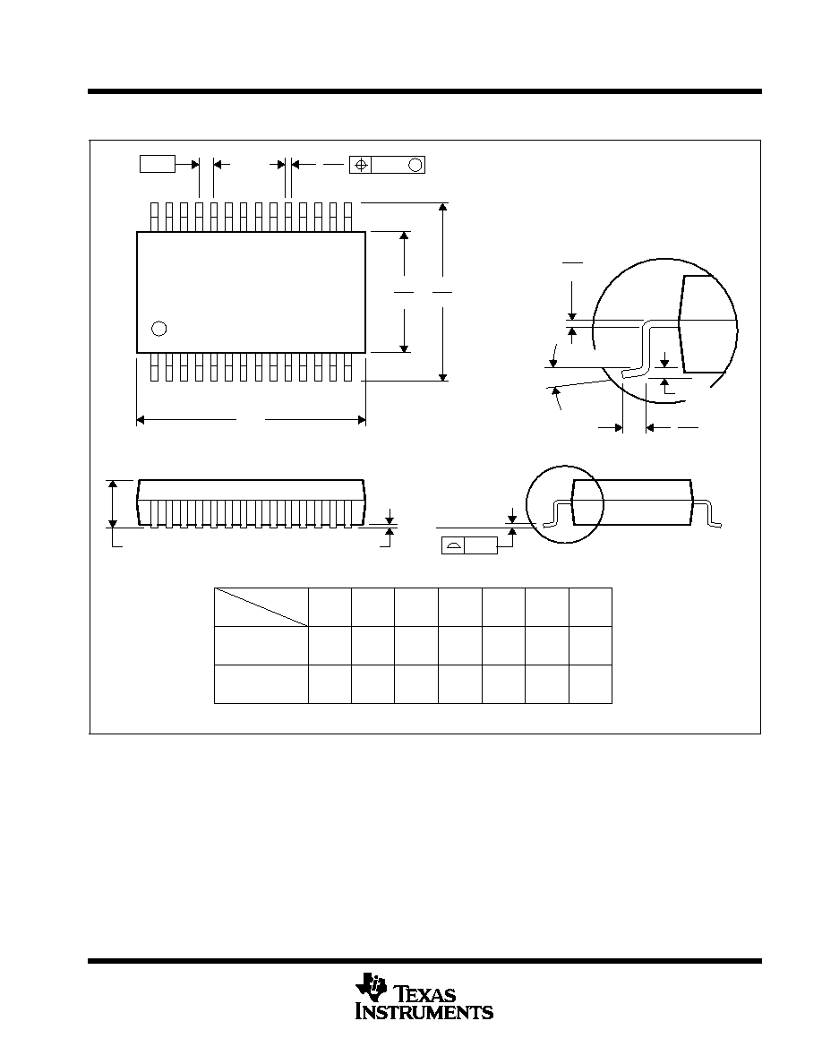
NOTES: A. All linear dimensions are in inches (millimeters).
B. This drawing is subject to change without notice.
C. Falls within JEDEC MS-001, except 18 and 20 pin minimum body lrngth (Dim A).
D. The 20 pin end lead shoulder width is a vendor option, either half or full width.
MECHANICAL DATA
MSOI003E ≠ JANUARY 1995 ≠ REVISED SEPTEMBER 2001
POST OFFICE BOX 655303
∑
DALLAS, TEXAS 75265
DW (R-PDSO-G**)
PLASTIC SMALL-OUTLINE PACKAGE
16 PINS SHOWN
0.419 (10,65)
0.400 (10,15)
0.291 (7,39)
0.299 (7,59)
16
0.400
(10,16)
A MIN
A MAX
(10,41)
0.410
0.462
(11,73)
(11,51)
0.453
18
0.610
(15,49)
(15,24)
0.600
24
DIM
PINS **
4040000/E 08/01
0.104 (2,65) MAX
0.004 (0,10)
0.012 (0,30)
Seating Plane
0
∞
≠ 8
∞
0.016 (0,40)
0.050 (1,27)
16
0.050 (1,27)
1
A
8
9
0.014 (0,35)
0.020 (0,51)
0.010 (0,25) NOM
Gage Plane
0.010 (0,25)
28
0.710
(18,03)
0.700
(17,78)
(12,70)
(12,95)
0.500
20
0.510
0.010 (0,25)
0.004 (0,10)
NOTES: A. All linear dimensions are in inches (millimeters).
B. This drawing is subject to change without notice.
C. Body dimensions do not include mold flash or protrusion not to exceed 0.006 (0,15).
D. Falls within JEDEC MS-013
MECHANICAL DATA
MSSO002E ≠ JANUARY 1995 ≠ REVISED DECEMBER 2001
POST OFFICE BOX 655303
∑
DALLAS, TEXAS 75265
DB (R-PDSO-G**)
PLASTIC SMALL-OUTLINE
4040065 /E 12/01
28 PINS SHOWN
Gage Plane
8,20
7,40
0,55
0,95
0,25
38
12,90
12,30
28
10,50
24
8,50
Seating Plane
9,90
7,90
30
10,50
9,90
0,38
5,60
5,00
15
0,22
14
A
28
1
20
16
6,50
6,50
14
0,05 MIN
5,90
5,90
DIM
A MAX
A MIN
PINS **
2,00 MAX
6,90
7,50
0,65
M
0,15
0
∞
≠ 8
∞
0,10
0,09
0,25
NOTES: A. All linear dimensions are in millimeters.
B. This drawing is subject to change without notice.
C. Body dimensions do not include mold flash or protrusion not to exceed 0,15.
D. Falls within JEDEC MO-150

IMPORTANT NOTICE
Texas Instruments Incorporated and its subsidiaries (TI) reserve the right to make corrections, modifications,
enhancements, improvements, and other changes to its products and services at any time and to discontinue
any product or service without notice. Customers should obtain the latest relevant information before placing
orders and should verify that such information is current and complete. All products are sold subject to TI's terms
and conditions of sale supplied at the time of order acknowledgment.
TI warrants performance of its hardware products to the specifications applicable at the time of sale in
accordance with TI's standard warranty. Testing and other quality control techniques are used to the extent TI
deems necessary to support this warranty. Except where mandated by government requirements, testing of all
parameters of each product is not necessarily performed.
TI assumes no liability for applications assistance or customer product design. Customers are responsible for
their products and applications using TI components. To minimize the risks associated with customer products
and applications, customers should provide adequate design and operating safeguards.
TI does not warrant or represent that any license, either express or implied, is granted under any TI patent right,
copyright, mask work right, or other TI intellectual property right relating to any combination, machine, or process
in which TI products or services are used. Information published by TI regarding third-party products or services
does not constitute a license from TI to use such products or services or a warranty or endorsement thereof.
Use of such information may require a license from a third party under the patents or other intellectual property
of the third party, or a license from TI under the patents or other intellectual property of TI.
Reproduction of information in TI data books or data sheets is permissible only if reproduction is without
alteration and is accompanied by all associated warranties, conditions, limitations, and notices. Reproduction
of this information with alteration is an unfair and deceptive business practice. TI is not responsible or liable for
such altered documentation.
Resale of TI products or services with statements different from or beyond the parameters stated by TI for that
product or service voids all express and any implied warranties for the associated TI product or service and
is an unfair and deceptive business practice. TI is not responsible or liable for any such statements.
Following are URLs where you can obtain information on other Texas Instruments products and application
solutions:
Products
Applications
Amplifiers
amplifier.ti.com
Audio
www.ti.com/audio
Data Converters
dataconverter.ti.com
Automotive
www.ti.com/automotive
DSP
dsp.ti.com
Broadband
www.ti.com/broadband
Interface
interface.ti.com
Digital Control
www.ti.com/digitalcontrol
Logic
logic.ti.com
Military
www.ti.com/military
Power Mgmt
power.ti.com
Optical Networking
www.ti.com/opticalnetwork
Microcontrollers
microcontroller.ti.com
Security
www.ti.com/security
Telephony
www.ti.com/telephony
Video & Imaging
www.ti.com/video
Wireless
www.ti.com/wireless
Mailing Address:
Texas Instruments
Post Office Box 655303 Dallas, Texas 75265
Copyright
2003, Texas Instruments Incorporated