SN75186
QUADRUPLE DRIVER/RECEIVER WITH LOOPBACK
SLLS068C ≠ FEBRUARY 1990 ≠ REVISED MAY 1995
1
POST OFFICE BOX 655303
∑
DALLAS, TEXAS 75265
D
Meets or Exceeds the Requirements of
ANSI EIA / TIA-232-E and ITU
Recommendation V.28
D
Four Independent Drivers and Receivers
D
Loopback Mode Functionally Self-Tests
Drivers and Receivers Without
Disconnection From Line
D
Driver Slew Rate Limited to 30 V/
µ
s Max
D
Built-In Receiver 1-
µ
s Noise Filter
D
Internal Thermal Overload Protection
D
EIA / TIA-232-E Inputs and Outputs
Withstand
±
30 V
D
Low Supply Current . . . 2.5 mA Typ
D
ESD Protection Exceeds 4000 V Per
MIL-STD-833C Method 3015
description
The SN75186 is a low-power bipolar device
containing four driver/receiver pairs designed to
interface data terminal equipment (DTE) with data
circuit-terminating equipment (DCE). Additionally,
the SN75186 has a loopback mode that can be
used by a data communication system to perform
a functional self-test on each driver/receiver pair,
removing the need to locally disconnect cables
and install a loopback connector. Flexibility of
control is ensured by each driver/receiver pair
having its own loopback control input. The
SN75186 is designed to conform to standards
ANSI EIA/ TIA-232-E and ITU Recommendation
V.28.
The maximum slew rate is limited to 30 V/
µ
s at
the driver outputs, and the SN75186 drives a capacitive load of 2500 pF at 20 kBaud. The receivers have input
filters that disregard input noise pulses shorter than 1
µ
s. The SN75186 is a robust device capable of
withstanding
±
30 V at driver outputs and at receiver inputs whether powered or unpowered. This device has
an internal ESD protection rated at 4 kV to prevent functional failures.
The SN75186 is characterized for operation from 0
∞
C to 70
∞
C.
Copyright
©
1995, Texas Instruments Incorporated
PRODUCTION DATA information is current as of publication date.
Products conform to specifications per the terms of Texas Instruments
standard warranty. Production processing does not necessarily include
testing of all parameters.
Please be aware that an important notice concerning availability, standard warranty, and use in critical applications of
Texas Instruments semiconductor products and disclaimers thereto appears at the end of this data sheet.
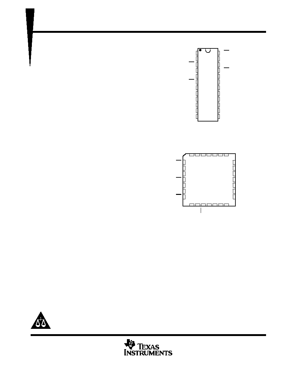
3 2 1 28 27
12 13
5
6
7
8
9
10
11
25
24
23
22
21
20
19
1Y
1B
2Y
2B
3Y
3B
4Y
1LB
2A
2Z
2LB
3A
3Z
3LB
4
26
14 15 16 17 18
4A
4Z
4LB
NC
V
GND
4B
1Z
1A
V
NC
NC
V
NC
FN PACKAGE
(TOP VIEW)
NC ≠ No internal connection
CC2
CC1
EE
1
2
3
4
5
6
7
8
9
10
11
12
24
23
22
21
20
19
18
17
16
15
14
13
3A
3Z
3LB
4A
4Z
4LB
V
EE
GND
4B
4Y
3B
3Y
2LB
2Z
2A
1LB
1Z
1A
V
CC2
V
CC1
1Y
1B
2Y
2B
DW PACKAGE
(TOP VIEW)
SN75186
QUADRUPLE DRIVER/RECEIVER WITH LOOPBACK
SLLS068C ≠ FEBRUARY 1990 ≠ REVISED MAY 1995
2
POST OFFICE BOX 655303
∑
DALLAS, TEXAS 75265
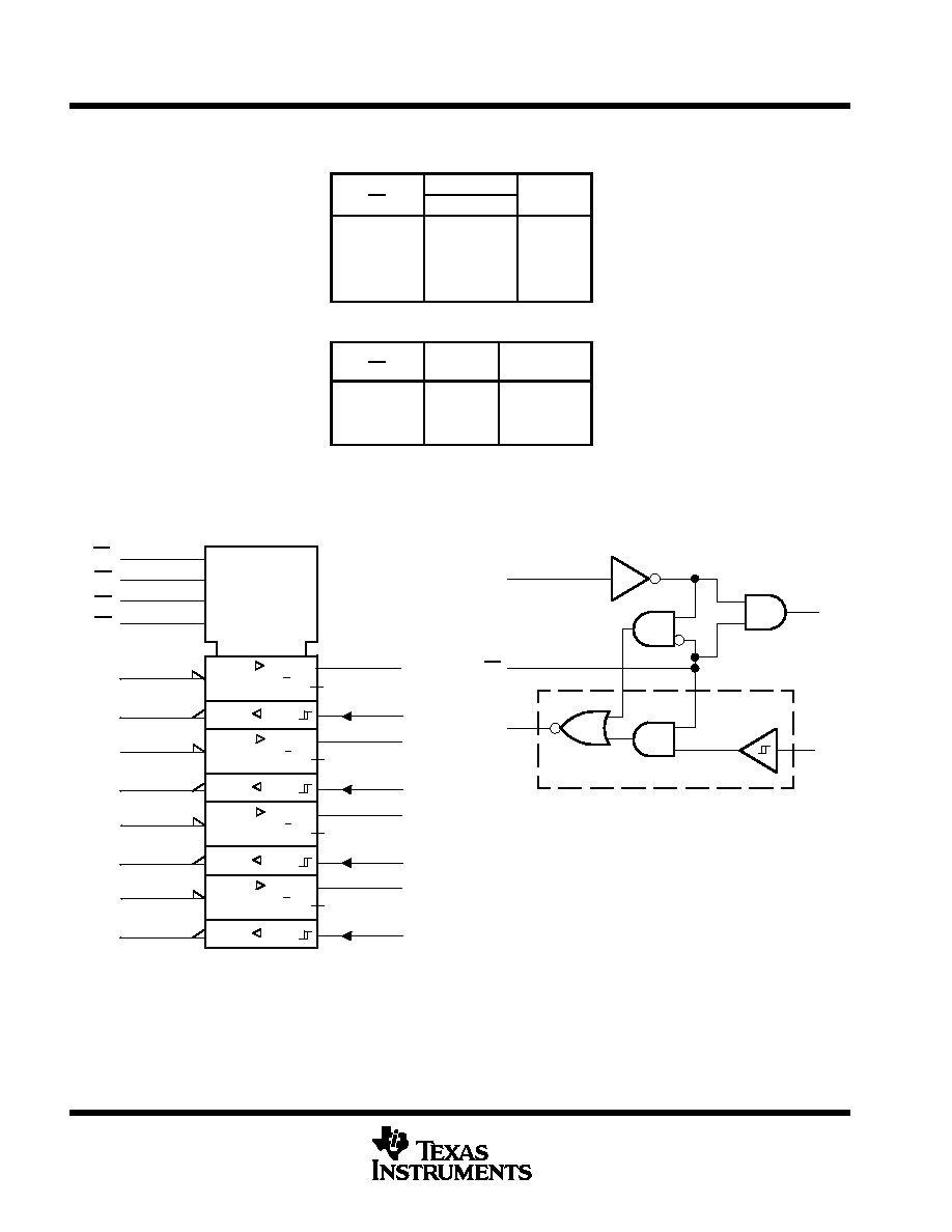
Function Tables
EACH RECEIVER
LOOPBACK
INPUTS
INPUT
LB
A
B
DE
H
X
H
L
H
X
L
H
L
L
X
L
L
H
X
H
EACH DRIVER
LOOPBACK
INPUT
OUTPUT
LB
A
Y
H
H
L
H
L
H
L
X
L
Voltages are EIA / TIA-232-E, and V.28 levels
H = high level, L = low level, X = irrelevant
logic symbol
G1
21
G2
24
G3
3
G4
6
1Y
16
1
1V5
19
1A
20
1Z
1B
15
1
2Y
14
2
2V6
22
2A
6
23
2Z
2B
13
2
3Y
12
3
3V7
1
3A
4Y
10
4
4V8
4
4A
8
5
4Z
4B
9
4
7
2
3Z
3B
11
3
1LB
2LB
3LB
4LB
This symbol is in accordance with ANSI/IEEE Std 91-1984 and
IEC Publication 617-12.
Pin numbers shown are for the DW package.
logic diagram, each driver/receiver pair
(positive logic)
Z
LB
A
Receiver
B
Y
Driver
SN75186
QUADRUPLE DRIVER/RECEIVER WITH LOOPBACK
SLLS068C ≠ FEBRUARY 1990 ≠ REVISED MAY 1995
3
POST OFFICE BOX 655303
∑
DALLAS, TEXAS 75265
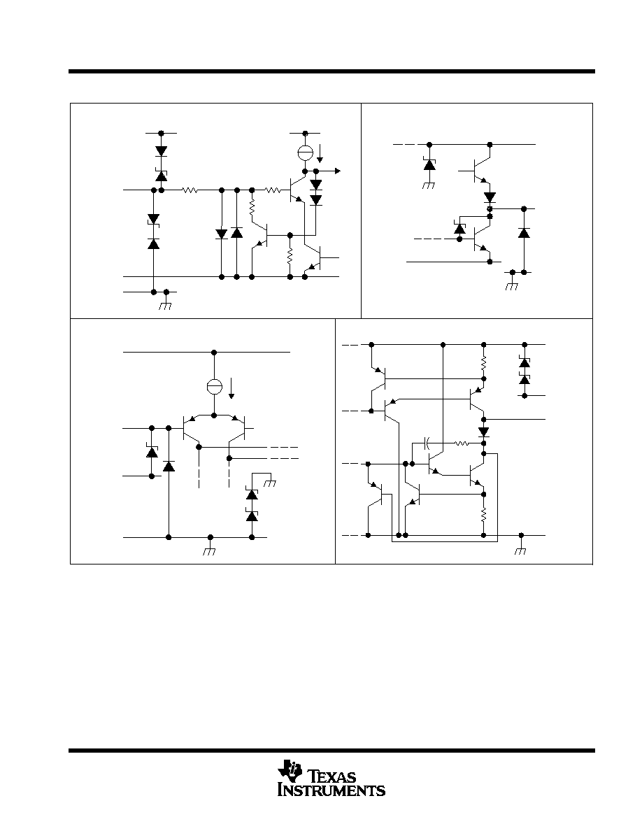
schematics of inputs and outputs
GND
8 V
8 V
GND
8 V
Internal
1.4-V Ref to GND
EQUIVALENT DRIVER AND LOOPBACK INPUT
EQUIVALENT DRIVER OUTPUT
D1
Output
GND
VCC1
3 pF
8 V
8 V
EQUIVALENT RECEIVER OUTPUT
8 V
8 V
GND
EQUIVALENT RECEIVER INPUT
GND
45 V
45 V
B Input
ESD Protection
GND
VCC2
VEE
Z Output
100 k
1.2 x VBE
ESD Protection
ESD Protection
VCC1
VCC2
2 k
2 k
4 k
VEE
VCC1
ESD Protection
A Input
VEE
ESD Protection
ESD
Protection
30
5 k
30
VEE
All component values shown are nominal.
SN75186
QUADRUPLE DRIVER/RECEIVER WITH LOOPBACK
SLLS068C ≠ FEBRUARY 1990 ≠ REVISED MAY 1995
4
POST OFFICE BOX 655303
∑
DALLAS, TEXAS 75265
absolute maximum ratings over operating free-air temperature range (unless otherwise noted)
Supply voltage, V
CC1
(see Note 1)
15 V
. . . . . . . . . . . . . . . . . . . . . . . . . . . . . . . . . . . . . . . . . . . . . . . . . . . . . . . . . . .
Supply voltage, V
CC2
7 V
. . . . . . . . . . . . . . . . . . . . . . . . . . . . . . . . . . . . . . . . . . . . . . . . . . . . . . . . . . . . . . . . . . . . . . .
Supply voltage, V
EE
≠ 15 V
. . . . . . . . . . . . . . . . . . . . . . . . . . . . . . . . . . . . . . . . . . . . . . . . . . . . . . . . . . . . . . . . . . . . . . .
Receiver input voltage range, V
I
≠ 30 V to 30 V
. . . . . . . . . . . . . . . . . . . . . . . . . . . . . . . . . . . . . . . . . . . . . . . . . . . . .
Driver input voltage range, V
I
(V
EE
+ 2 V) to V
CC1
. . . . . . . . . . . . . . . . . . . . . . . . . . . . . . . . . . . . . . . . . . . . . . . . . .
Loopback input voltage range, V
I
0 V to 7 V
. . . . . . . . . . . . . . . . . . . . . . . . . . . . . . . . . . . . . . . . . . . . . . . . . . . . . . .
Driver output voltage range, V
O
≠ 30 V to 30 V
. . . . . . . . . . . . . . . . . . . . . . . . . . . . . . . . . . . . . . . . . . . . . . . . . . . . . .
Continuous total power dissipation
See Dissipation Rating Table
. . . . . . . . . . . . . . . . . . . . . . . . . . . . . . . . . . . . .
Operating free-air temperature range, T
A
0
∞
C to 70
∞
C
. . . . . . . . . . . . . . . . . . . . . . . . . . . . . . . . . . . . . . . . . . . . . .
Storage temperature range, T
stg
≠ 65
∞
C to 150
∞
C
. . . . . . . . . . . . . . . . . . . . . . . . . . . . . . . . . . . . . . . . . . . . . . . . . . .
Case temperature for 10 seconds: FN package
260
∞
C
. . . . . . . . . . . . . . . . . . . . . . . . . . . . . . . . . . . . . . . . . . . . . .
Lead temperature 1,6 mm (1/16 inch) from case for 10 seconds: DW package
260
∞
C
. . . . . . . . . . . . . . . . . . .
Stresses beyond those listed under "absolute maximum ratings" may cause permanent damage to the device. These are stress ratings only, and
functional operation of the device at these or any other conditions beyond those indicated under "recommended operating conditions" is not
implied. Exposure to absolute-maximum-rated conditions for extended periods may affect device reliability.
NOTE 1: All voltages are with respect to the network ground terminal.
DISSIPATION RATING TABLE
PACKAGE
TA
25
∞
C
POWER RATING
DERATING FACTOR
ABOVE TA = 25
∞
C
TA = 70
∞
C
POWER RATING
DW
1350 mW
10.8 mW/
∞
C
864 mW
FN
1400 mW
11.2 mW/
∞
C
896 mW
recommended operating conditions
MIN
NOM
MAX
UNIT
Supply voltage, VCC1
10.8
12
13.2
V
Supply voltage, VCC2
4.5
5
5.5
V
Supply voltage, VEE
≠10.8
≠12
≠13.2
V
Input voltage, VI
Driver and loopback
0
VCC2
V
Input voltage, VI (see Note 2)
Receiver
±
30
V
High-level input voltage, VIH
Driver and loopback
2
V
Low-level input voltage, VIL
Driver and loopback
0.8
V
Output voltage powered on or off, VO
Driver
±
30
V
High-level output current, IOH
Receiver
≠ 4
mA
Low-level output current, IOL
Receiver
4
mA
Operating free-air temperature, TA
0
70
∞
C
NOTE 2: If all receiver inputs are held at
±
30 V, the thermal dissipation limit of the package may be exceeded. The thermal shutdown may not
protect the device, as this dissipation occurs in the receiver input resistors.
SN75186
QUADRUPLE DRIVER/RECEIVER WITH LOOPBACK
SLLS068C ≠ FEBRUARY 1990 ≠ REVISED MAY 1995
5
POST OFFICE BOX 655303
∑
DALLAS, TEXAS 75265
DRIVER SECTION
electrical characteristics over full recommended ranges of supply voltage and operating free-air
temperature (unless otherwise noted)
PARAMETER
TEST CONDITIONS
MIN
TYP
MAX
UNIT
VOH
High-level output voltage
RL = 3 k
,
VIL = 0.8 V,
See Figure 1
7
V
VOL
Low-level output voltage
RL = 3 k
,
VIH = 2 V,
See Figure 1
≠ 7
V
VOH(LB)
High-level output voltage in
loopback modeß∂
RL = 3 k
,
LB at 0.8 V,
VIL = 0.8 V
≠ 7
V
IIH
High-level input current
(driver and loopback inputs)#
VI = 5 V,
See Figure 2
100
µ
A
IIL
Low-level input current
(driver and loopback inputs)#
≠ 100
µ
A
VOS(H)
High-level short-circuit output
current
VI = 0.8 V,
VO = 0,
See Note 3 and Figure 1
≠ 10
≠ 20
≠ 35
mA
VOS(L)
Low-level short-circuit output
current
VI = 2 V,
VO = 0,
See Note 3 and Figure 1
10
20
35
mA
ICC1
Supply current from VCC1
No load
2.5
4
mA
ICC1(LB)
Supply current from VCC1 with
loopback on
No load,
LB at 0.8 V
10
mA
IEE
Supply current from VEE
No load
≠ 2.5
≠ 4
mA
IEE(LB)
Supply current from VEE with
loopback on
No load,
LB at 0.8 V
≠ 10
mA
ICC2
Supply current from VCC2
No load,
VI = 0,
See Note 5
≠ 10
≠ 100
µ
A
ICC2(LB)
Supply current from VCC2 with
loopback on
No load,
See Note 5
LB at 0.8 V,
VI = 0,
≠ 10
≠ 100
µ
A
ro
Output resistance
VCC1 = VEE = VCC2 = 0,
See Note 4
VO = ≠ 2 V to 2 V,
0.3
5
k
All typical values are at TA = 25
∞
C.
The algebraic convention, where the more positive (less negative) limit is designated as maximum, is used in this data sheet for logic levels only.
ß This is the most positive level to which the driver output rises when the device is in the loopback mode and the driver input is at a low level.
∂ The loopback mode should be entered only when the driver output is in the low (marking) state.
# Unused driver inputs should be tied to 0 V or VCC2; unused loopback inputs should be tied to VCC2.
NOTES:
3. Minimum IOS(H) and IOS(L) are specified at VO = 0, as this more accurately describes the output current needed to dynamically drive
capacitive lines. A minimum of
±
10 mA is sufficient to drive 2500 pF in parallel with 3 k
at a slew rate of 4 V/
µ
s ( in accordance
with EIA / TIA-232-E and V.28).
4. Test conditions are those specified by EIA / TIA-232-E.
5. Without a load and VI = 0, the worst-case conditions, VCC2 sources a small current originating from VCC1 giving ICC2 supply current
a negative sign. When a receiver has an output load, VCC2 sinks static and dynamic supply currents to meet load requirements.