TAS5112
SLES048B - JULY 2003
DIGITAL AMPLIFIER POWER STAGE
FEATURES
D
50 W per Channel (BTL) Into 6
(Stereo)
D
95 dB Dynamic Range With TAS5026
D
Less Than 0.1% THD+N (TDAA System ≠ 1 W
RMS Into 6
)
D
Less Than 0.2% THD+N (TDAA System ≠ 50 W
RMS into 6
)
D
Power Efficiency Typically 90% Into 6-
Load
D
Self-Protecting Design (Undervoltage,
Overtemperature and Short Conditions) With
Error Reporting
D
Internal Gate Drive Supply Voltage Regulator
D
EMI Compliant When Used With
Recommended System Design
APPLICATIONS
D
DVD Receiver
D
Home Theatre
D
Mini/Micro Component Systems
D
Internet Music Appliance
DESCRIPTION
The TAS5112 is a high-performance, integrated stereo
digital amplifier power stage designed to drive 6-
speakers at up to 50 W per channel. The device
incorporates TI's PurePath Digital
t
technology and is
used in conjunction with a digital audio PWM processor
(TAS50XX) and a simple passive demodulation filter to
deliver high-quality, high-efficiency, true-digital audio
amplification.
The efficiency of this digital amplifier is typically 90%,
reducing the size of both the power supplies and heat sinks
needed. Overcurrent protection, overtemperature
protection, and undervoltage protection are built into the
TAS5112, safeguarding the device and speakers against
fault conditions that could damage the system.
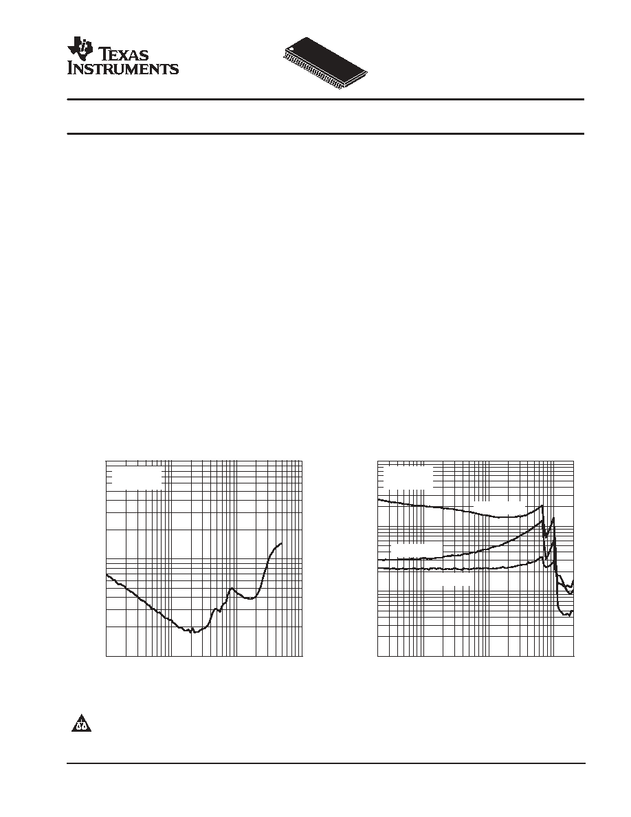
PO - Output Power - W
100m
RL = 6
TC = 75
∞
C
1
10
100
0.01
0.1
1
THD+N - T
otal Harmonic Distortion + Noise - %
THD + NOISE vs OUTPUT POWER
f - Frequency - Hz
20
100
1k
10k
THD+N - T
otal Harmonic Distortion + Noise - %
0.001
0.1
1
20k
RL = 6
TC = 75
∞
C
0.01
THD + NOISE vs FREQUENCY
PO = 50 W
PO = 1 W
PO = 10 W
PurePath Digital and PowerPAD are trademarks of Texas Instruments.
Other trademarks are the property of their respective owners.
PRODUCTION DATA information is current as of publication date. Products
conform to specifications per the terms of Texas Instruments standard warranty.
Production processing does not necessarily include testing of all parameters.
Please be aware that an important notice concerning availability, standard warranty, and use in critical applications of Texas Instruments
semiconductor products and disclaimers thereto appears at the end of this data sheet.
www.ti.com
Copyright
2003, Texas Instruments Incorporated
TAS5112
SLES048B - JULY 2003
www.ti.com
2
These devices have limited built-in ESD protection. The leads should be shorted together or the device placed in conductive foam during
storage or handling to prevent electrostatic damage to the MOS gates.
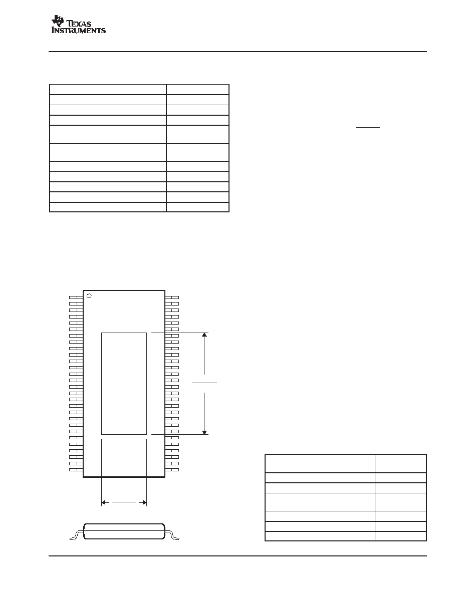
GENERAL INFORMATION
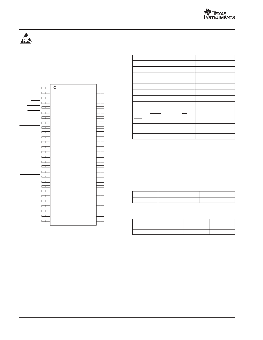
Terminal Assignment
The TAS5112 is offered in a thermally enhanced 56-pin
TSSOP DFD (thermal pad is on the top), shown as follows.
1
2
3
4
5
6
7
8
9
10
11
12
13
14
15
16
17
18
19
20
21
22
23
24
25
26
27
28
56
55
54
53
52
51
50
49
48
47
46
45
44
43
42
41
40
39
38
37
36
35
34
33
32
31
30
29
GND
GND
GREG
OTW
SD_CD
SD_AB
PWM_DP
PWM_DM
RESET_CD
PWM_CM
PWM_CP
DREG_RTN
M3
M2
M1
DREG
PWM_BP
PWM_BM
RESET_AB
PWM_AM
PWM_AP
GND
DGND
GND
DVDD
GREG
GND
GND
GND
GVDD
BST_D
PVDD_D
PVDD_D
OUT_D
OUT_D
GND
GND
OUT_C
OUT_C
PVDD_C
PVDD_C
BST_C
BST_B
PVDD_B
PVDD_B
OUT_B
OUT_B
GND
GND
OUT_A
OUT_A
PVDD_A
PVDD_A
BST_A
GVDD
GND
DFD PACKAGE
(TOP VIEW)
ABSOLUTE MAXIMUM RATINGS
over operating free-air temperature range unless otherwise noted(1)
TAS5112
UNITS
DVDD TO DGND
≠0.3 V to 4.2 V
GVDD TO GND
33.5 V
PVDD_X TO GND (dc voltage)
33.5 V
PVDD_X TO GND (spike voltage(2))
48 V
OUT_X TO GND (dc voltage)
33.5 V
OUT_X TO GND (spike voltage(2))
48 V
BST_X TO GND (dc voltage)
48 V
BST_X TO GND (spike voltage(2))
53 V
GREG TO GND (3)
14.2 V
PWM_XP, RESET, M1, M2, M3, SD,
OTW
≠0.3 V to DVDD + 0.3 V
Maximum operating junction
temperature, TJ
≠40
∞
C to 150
∞
C
Storage temperature
≠40
∞
C to 125
∞
C
(1) Stresses beyond those listed under "absolute maximum ratings"
may cause permanent damage to the device. These are stress
ratings only, and functional operation of the device at these or any
other conditions beyond those indicated under "recommended
operating conditions" is not implied. Exposure to absolute-
maximum-rated conditions for extended periods may affect device
reliability.
(2) The duration of voltage spike should be less than 100 ns.
(3) GREG is treated as an input when the GREG pin is overdriven by
GVDD of 12 V.
ORDERING INFORMATION
TA
PACKAGE
DESCRIPTION
0
∞
C to 70
∞
C
TAS5112DFD
56-pin small TSSOP
(1) For the most current specification and package information, refer to
our web site at www.ti.com.
PACKAGE DISSIPATION RATINGS
PACKAGE
R
JC
(
∞
C/W)
R
JA
(
∞
C/W)
56-pin DAD TSSOP
1.14
See Note 1
(1) The TAS5112 package is thermally enhanced for conductive
cooling using an exposed metal pad area. It is impractical to use the
device with the pad exposed to ambient air as the only heat sinking
of the device.
For this reason, R
JA a system parameter that characterizes the
thermal treatment provided in the application. An example and
discussion of typical system R
JA values are provided in the
Thermal Information section. This example provides additional
information regarding the power dissipation ratings. This example
should be used as a reference to calculate the heat dissipation
ratings for a specific application. TI application engineering
provides technical support to design heat sinks if needed.
TAS5112
SLES048B - JULY 2003
www.ti.com
3
Terminal Functions
TERMINAL
FUNCTION(1)
DESCRIPTION
NAME
NO.
FUNCTION(1)
DESCRIPTION
BST_A
31
P
High side bootstrap supply (BST), external capacitor to OUT_A required
BST_B
42
P
High side bootstrap supply (BST), external capacitor to OUT_B required
BST_C
43
P
HS bootstrap supply (BST), external capacitor to OUT_C required
BST_D
54
P
HS bootstrap supply (BST), external capacitor to OUT_D required
DGND
23
P
Digital I/O reference ground
DREG
16
P
Digital supply voltage regulator decoupling pin, capacitor connected to GND
DREG_RTN
12
P
Digital supply voltage regulator decoupling return pin
DVDD
25
P
I/O reference supply input (3.3V)
GND
1, 2, 22, 24,
28, 29, 27, 36,
37, 48, 49, 56
P
Power ground
GREG
3, 26
P
Gate drive voltage regulator decoupling pin, capacitor to REG_GND
GVDD
30, 55
P
Voltage supply to on-chip gate drive and digital supply voltage regulators
M1 (TST0)
15
I
Mode selection pin
M2
14
I
Mode selection pin
M3
13
I
Mode selection pin
OTW
4
O
Overtemperature warning output, open drain with internal pullup
OUT_A
34, 35
O
Output, half-bridge A
OUT_B
38, 39
O
Output, half-bridge B
OUT_C
46, 47
O
Output, half-bridge C
OUT_D
50, 51
O
Output, half-bridge D
PVDD_A
32, 33
P
Power supply input for half-bridge A
PVDD_B
40, 41
P
Power supply input for half-bridge B
PVDD_C
44, 45
P
Power supply input for half-bridge C
PVDD_D
52, 53
P
Power supply input for half-bridge D
PWM_AM
20
I
Input signal (negative), half-bridge A
PWM_AP
21
I
Input signal (positive), half-bridge A
PWM_BM
18
I
Input signal (negative), half-bridge B
PWM_BP
17
I
Input signal (positive), half-bridge B
PWM_CM
10
I
Input signal (negative), half-bridge C
PWM_CP
11
I
Input signal (positive), half-bridge C
PWM_DM
8
I
Input signal (negative), half-bridge D
PWM_DP
7
I
Input signal (positive), half-bridge D
RESET_AB
19
I
Reset signal, active low
RESET_CD
9
I
Reset signal, active low
SD_AB
6
O
Shutdown signal for half-bridges A and B
SD_CD
5
O
Shutdown signal for half-bridges C and D
(1) I = input, O = Output, P = Power
TAS5112
SLES048B - JULY 2003
www.ti.com
4
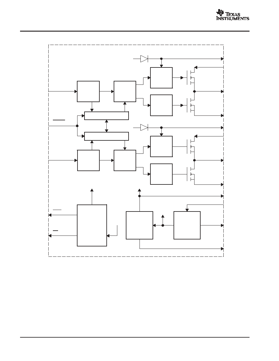
FUNCTIONAL BLOCK DIAGRAM
GREG
GVDD
GREG
DREG_RTN
Timing
Control
Gate
Drive
PWM_AP
OUT_A
GND
PVDD_A
BST_A
PWM
Receiver
OUT_B
GND
PVDD_B
GREG
Protection A
Protection B
PWM_BP
RESET
GREG
BST_B
DREG
To Protection
Blocks
OTW
SD
DREG
DREG_RTN
GREG
DREG
Gate
Drive
Gate
Drive
Gate
Drive
GREG
OT
Protection
UVP
PWM
Receiver
Timing
Control
This diagram shows one channel.

TAS5112
SLES048B - JULY 2003
www.ti.com
5
RECOMMENDED OPERATING CONDITIONS
MIN
TYP
MAX
UNIT
DVDD
Digital supply (1)
Relative to DGND
3
3.3
3.6
V
GVDD
Supply for internal gate drive and logic
regulators
Relative to GND
16
29.5
30.5
V
PVDD_x
Half-bridge supply
Relative to GND, RL= 6
to 8
0
29.5
30.5
V
TJ
Junction temperature
0
125
_
C
(1) It is recommended for DVDD to be connected to DREG via a 100-
resistor.
ELECTRICAL CHARACTERISTICS
PVDD_X = 29.5 V, GVDD = 29.5 V, DVDD connected to DREG via a 100-
resistor, RL = 6
, 8X fs = 384 kHz, unless otherwise noted
TYPICAL
OVER TEMPERATURE
SYMBOL
PARAMETER
TEST CONDITIONS
TA=25
∞
C
TA=25
∞
C
TCase=
75
∞
C
TA=40
∞
C
TO 85
∞
C
UNITS
MIN/TYP/
MAX
AC PERFORMANCE, BTL Mode, 1 kHz
RL = 8
, THD = 0.2%,
AES17 filter, 1 kHz
40
W
Typ
Po
Output power
RL = 8
, THD = 10%, AES17
filter, 1 kHz
50
W
Typ
Po
Output power
RL = 6
, THD = 0.2%,
AES17 filter, 1 kHz
50
W
Typ
RL = 6
, THD = 10%, AES17
filter, 1 kHz
62
W
Typ
Po = 1 W/ channel, RL = 6
,
AES17 filter
0.03%
Typ
THD+N
Total harmonic distortion
+ noise
Po = 10 W/channel, RL = 6
,
AES17 filter
0.04%
Typ
+ noise
Po = 50 W/channel, RL = 6
,
AES17 filter
0.2%
Typ
Vn
Output integrated voltage
noise
A-weighted, mute, RL = 6
,,
20 Hz to 20 kHz, AES17 filter
260
µ
V
Max
SNR
Signal-to-noise ratio
A-weighted, AES17 filter
96
dB
Typ
DR
Dynamic range
f = 1 kHz, A-weighted,
AES17 filter
96
dB
Typ
INTERNAL VOLTAGE REGULATOR
DREG
Voltage regulator
Io = 1 mA,
PVDD = 18 V-30.5 V
3.1
V
Typ
GREG
Voltage regulator
Io = 1.2 mA,
PVDD = 18 V-30.5 V
13.4
V
Typ
IVGDD
GVDD supply current,
operating
fS = 384 kHz, no load, 50%
duty cycle
24
mA
Max
IDVDD
DVDD supply current,
operating
fS = 384 kHz, no load
1
5
mA
Max
OUTPUT STAGE MOSFETs
Ron,LS
Forward on-resistance,
low side
TJ = 25
∞
C
155
m
Typ
Ron,HS
Forward on-resistance,
high side
TJ = 25
∞
C
155
m
Typ
TAS5112
SLES048B - JULY 2003
www.ti.com
6
ELECTRICAL CHARACTERISTICS
PVDD_x = 29.5 V, GVDD = 29.5 V, DVDD connected to DREG via a 100-
resistor, RL = 6
, 8X fs = 384 kHz, unless otherwise noted
TYPICAL
OVER TEMPERATURE
SYMBOL
PARAMETER
TEST CONDITIONS
TA=25
∞
C
TA=25
∞
C
TCase=
75
∞
C
TA=40
∞
C
TO 85
∞
C
UNITS
MIN/TYP/
MAX
INPUT/OUTPUT PROTECTION
Vuvp,G
Undervoltage protection
Set the DUT in normal
operation mode with all the
protections enabled. Sweep
GVDD up and down. Monitor
7.4
6.9
V
Min
Vuvp,G
Undervoltage protection
limit, GVDD
GVDD up and down. Monitor
SD output. Record the
GREG reading when SD is
triggered.
7.4
7.9
V
Max
OTW
Overtemperature warning,
junction temperature
125
∞
C
Typ
OTE
Overtemperature error,
junction temperature
150
∞
C
Typ
OC
Overcurrent protection
See Note 1.
5.8
A
Typ
STATIC DIGITAL SPECIFICATION
PWM_AP, PWM_BP, M1,
M2, M3, SD, OTW
VIH
High-level input voltage
2
V
Min
VIH
High-level input voltage
DVDD
V
Max
VIL
Low-level input voltage
0.8
V
Max
Leakage
Input leakage current
-10
µ
A
Min
Leakage
Input leakage current
10
µ
A
Max
OTW/SHUTDOWN (SD)
Internally pull up R from
OTW/SD to DVDD
30
22.5
k
Min
VOL
Low level output voltage
IO = 4 mA
0.4
V
Max
(1) To optimize device performance and prevent overcurrent (OC) protection tripping, the demodulation filter must be designed with special care. See
Demodulation Filter Design in the Application Information section of the data sheet and consider the recommended inductors and capacitors for
optimal performance. It is also important to consider PCB design and layout for optimum performance of the TAS5112. It is recommended to follow
the TAS5112F2EVM (S/N 112) design and layout guidelines for best performance.
TAS5112
SLES048B - JULY 2003
www.ti.com
7
SYSTEM CONFIGURATION USED FOR CHARACTERIZATION
TAS5112DFD
VALID_1
42
41
4
13
11
10
9
8
7
PWM PROCESSOR
TAS5026
GVDD
OUT_C
BST_D
PVDD_C
GND
PVDD_D
PVDD_D
PVDD_C
OUT_D
52
53
55
OUT_D
54
GND
OUT_C
56
51
49
47
50
48
BST_C
BST_B
PVDD_B
44
46
43
45
6
14
15
16
12
5
1
2
3
10
µ
H
10
µ
H
470 nF
4.7 k
1000
µ
F
100 nF
PWM_AP_1
PWM_AM_1
100 nF
100 nF
1.5
100 nF
33 nF
H-Bridge
Power Supply
Gate-Drive
Power Supply
External Power Supply
4.7 k
LPCB
DREG
SD_CD
M1
PWM_CM
RESET_CD
PWM_DP
SD_AB
PWM_DM
GREG
M2
M3
DREG_RTN
PWM_CP
OTW
GND
GND
LPCB : TRACK IN THE PCB (1.0 mm wide and 50 mm long)
{
Voltage Suppressor Diode: 1SMA33CAT
GND
LPCB
33 nF
100 nF
1.5
PVDD_B
PVDD_A
OUT_B
GND
OUT_A
GND
OUT_B
GVDD
OUT_A
GND
PVDD_A
BST_A
37
38
40
39
36
34
32
35
33
29
31
30
10
µ
H
10
µ
H
470 nF
4.7 k
1000
µ
F
100 nF
100 nF
1.5
100 nF
33 nF
4.7 k
LPCB
LPCB
33 nF
100 nF
1.5
100 nF
GND
PWM_BP
GND
GND
PWM_AP
RESET_AB
PWM_BM
PWM_AM
GREG
DVDD
GND
DGND
25
23
22
21
20
19
18
26
27
28
24
17
1
µ
F
ERR_RCVY
100 nF
VALID_2
PWM_AP_2
PWM_AM_2
100
100 nF
1
µ
F
1.5
1.5
1.5
{
{
{
{
TAS5112
SLES048B - JULY 2003
www.ti.com
8
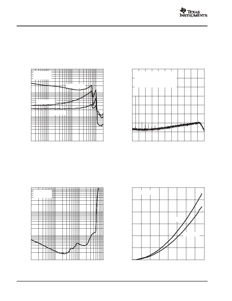
TYPICAL CHARACTERISTICS AND SYSTEM PERFORMANCE
OF TAS5112 EVM WITH TAS5026 PWM PROCESSOR
Figure 1
f - Frequency - Hz
20
100
1k
10k
THD+N - T
otal Harmonic Distortion + Noise - %
TOTAL HARMONIC DISTORTION + NOISE
vs
FREQUENCY
0.001
0.1
1
20k
RL = 6
TC = 75
∞
C
0.01
PO = 50 W
PO = 1 W
PO = 10 W
Figure 2
f - Frequency - kHz
-160
-140
-120
-100
-80
-60
-40
-20
0
0
2
4
6
8
10
12
14
16
18
20
22
RL = 6
FFT = -60 dB
TC = 75
∞
C
TAS5026 Front End Device
Noise Amplitude - dBr
NOISE AMPLITUDE
vs
FREQUENCY
Figure 3
PO - Output Power - W
100m
RL = 6
TC = 75
∞
C
1
10
100
THD+N - T
otal Harmonic Distortion + Noise - %
TOTAL HARMONIC DISTORTION + NOISE
vs
OUTPUT POWER
0.01
0.1
10
1
Figure 4
VDD - Supply Voltage - V
0
10
20
30
40
50
60
0
4
8
12
16
20
24
28
32
TA = 75
∞
C
P
O
- Output Power - W
OUTPUT POWER
vs
H-BRIDGE VOLTAGE
RL = 6
RL = 8
TAS5112
SLES048B - JULY 2003
www.ti.com
9
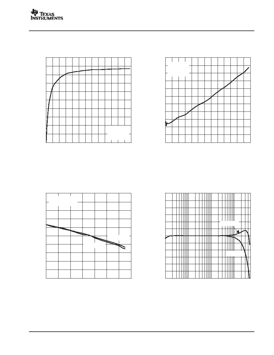
Figure 5
PO - Output Power - W
0
10
20
30
40
50
60
70
80
90
100
0
5
10 15 20 25 30 35 40 45 50 55 60 65
f = 1 kHz
RL = 6
TC = 75
∞
C
- System Output Stage Efficiency - %
SYSTEM OUTPUT STAGE EFFICIENCY
vs
OUTPUT POWER
Figure 6
PO - Output Power - W
0
1
2
3
4
5
6
7
8
9
10
11
0
5
10 15 20 25 30 35 40 45 50 55 60 65
f = 1 kHz
RL = 6
TC = 75
∞
C
P
to
t - Power Loss - W
POWER LOSS
vs
OUTPUT POWER
Figure 7
TC - Case Temperature -
∞
C
40
42
44
46
48
50
52
54
56
58
60
0
20
40
60
80
100
120
140
PVDD = 29.5 V
RL = 6
P
O
- Output Power - W
OUTPUT POWER
vs
CASE TEMPERATURE
Channel 1
Channel 2
-3.0
-2.5
-2.0
-1.5
-1.0
-0.5
0.0
0.5
1.0
1.5
2.0
2.5
3.0
f - Frequency - Hz
Amplitude - dBr
10
100
1k
50k
10k
Figure 8
RL = 8
AMPLITUDE
vs
FREQUENCY
RL = 6
TAS5112
SLES048B - JULY 2003
www.ti.com
10
Figure 9
TJ - Junction Temperature -
∞
C
120
130
140
150
160
170
180
190
200
0
10
20
30
40
50
60
70
80
90
100
r on
- On-State Resistance - m
ON-STATE RESISTANCE
vs
JUNCTION TEMPERATURE
TAS5112
SLES048B - JULY 2003
www.ti.com
11
THEORY OF OPERATION
POWER SUPPLIES
The power device only requires two supply voltages,
GVDD and PVDD_X.
GVDD is the gate drive supply for the device, regulated
internally down to approximately 12 V, and decoupled with
regards to board GND on the GREG pins through an
external capacitor. GREG powers both the low side and
high side via a bootstrap step-up conversion. The
bootstrap supply is charged after the first low-side turn-on
pulse. Internal digital core voltage DREG is also derived
from GVDD and regulated down by internal circuitry to
3.3 V.
The gate-driver regulator can be bypassed for reducing
idle loss in the device by shorting GREG to GVDD and
directly feeding in 12.0 V. This can be useful in an
application where thermal conduction of heat from the
device is difficult.
PVDD_X is the H-bridge power supply pin. Two power pins
exists for each half-bridge to handle the current density. It
is very important that the circuitry recommendations
around the PVDD_X pins are followed very carefully both
topology- and layout-wise. For topology
recommendations, see the Typical System Configuration
section. Following these recommendations is important for
parameters like EMI, reliability, and performance.
POWERING UP
RESET
GVDD
PVDD_x
PWM_xP
> 1 ms
> 1 ms
NOTE: PVDD should not be powered up before GVDD.
During power up when RESET is asserted LOW, all
MOSFETs are turned off and the two internal half-bridges
are in the high-impedance state (Hi-Z). The bootstrap
capacitors supplying high-side gate drive are at this point
not charged. To comply with the click and pop scheme and
use of non-TI TDAA modulators it is recommended to use
a 4-k
pulldown resistor on each PWM output node to
ground. This precharges the bootstrap supply capacitors
and discharges the output filter capacitor (see the Typical
TAS5112 Application Configuration section).
After GVDD has been applied, it takes approximately 800
µ
s to fully charge the BST capacitor. Within this time,
RESET must be kept low. After approximately 1 ms, the
back-end bootstrap capacitor is charged.
RESET can now be released if the modulator is powered
up and streaming valid PWM signals to the back-end
PWM_xP. Valid means a switching PWM signal which
complies with the frequency and duty cycle ranges stated
in the Recommended Operating Conditions.
A constant HIGH dc level on the PWM_xP is not permitted,
because it would force the high-side MOSFET ON until it
eventually ran out of BST capacitor energy and might
damage the device.
An unknown state of the PWM output signals from the
modulator is illegal and should be avoided, which in
practice means that the PWM processor must be powered
up and initialized before RESET is de-asserted HIGH to
the back end.
POWERING DOWN
For power down of the back end, an opposite approach is
necessary. The RESET must be asserted LOW before the
valid PWM signal is removed.
When PWM processors are used in conjunction with TI
TDAA back ends, the correct timing control of RESET and
PWM_xP is performed by the modulator.
PRECAUTION
The TAS5112 must always start up in the high-impedance
(Hi-Z) state. In this state, the bootstrap (BST) capacitor is
precharged by a resistor on each PWM output node to
ground. See the system configuration. This ensures that
the back end is ready for receiving PWM pulses, indicating
either HIGH- or LOW-side turnon after RESET is
deasserted to the back end.
With the following pulldown and BST capacitor size the
charge time is:
C = 33 nF, R = 4.7
k
R
◊
C
◊
5 = 775.5
µ
s
After GVDD has been applied, it takes approximately 800
µ
s to fully charge the BST capacitor. During this time,
RESET must be kept low. After approximately 1 ms the
back end BST is charged and ready. RESET can now be
released if the PWM modulator is ready and is streaming
valid PWM signals to the back end. Valid PWM signals are
switching PWM signals with a frequency between
350-400 kHz. A constant HIGH level on the PWM+ would
force the high side MOSFET ON until it eventually ran out
of BST capacitor energy. Putting the device in this
condition should be avoided.
TAS5112
SLES048B - JULY 2003
www.ti.com
12
In practice this means that the DVDD-to-PWM processor
(front-end) should be stable and initialization should be
completed before RESET is deasserted to the back end.
CONTROL I/O
Shutdown Pin: SD
The SD pin functions as an output pin and is intended for
protection-mode signaling to, for example, a controller or
other front-end device. The pin is open-drain with an
internal pullup to DVDD.
The logic output is, as shown in the following table, a
combination of the device state and RESET input:
SD
RESET
DESCRIPTION
0
0
Not used
0
1
Device in protection mode, i.e., UVP and/or OC
and/or OT error
1(1)
0
Device set high-impedance (Hi-Z), SD forced high
1
1
Normal operation
(1) SD is pulled high when RESET is asserted low independent
of chip state (i.e., protection mode). This is desirable to
maintain compatibility with some TI PWM front ends.
Temperature Warning Pin: OTW
The OTW pin gives a temperature warning signal when
temperature exceeds the set limit. The pin is of the
open-drain type with an internal pullup to DVDD.
OTW
DESCRIPTION
0
Junction temperature higher than 125
∞
C
1
Junction temperature lower than 125
∞
C
Overall Reporting
The SD pin, together with the OTW pin, gives chip state
information as described in Table 1.
Table 1. Error Signal Decoding
OTW
SD
DESCRIPTION
0
0
Overtemperature error (OTE)
0
1
Overtemperature warning (OTW)
1
0
Overcurrent (OC) or undervoltage (UVP) error
1
1
Normal operation, no errors/warnings
Chip Protection
The TAS5112 protection function is implemented in a
closed loop with, for example, a system controller and TI
PWM processor. The TAS5112 contains three individual
systems protecting the device against error conditions. All
of the error events covered result in the output stage being
set in a high-impedance state (Hi-Z) for maximum
protection of the device and connected equipment.
The device can be recovered by toggling RESET low and
then high, after all errors are cleared.
Overcurrent (OC) Protection
The device has individual forward current protection on
both high-side and low-side power stage FETs. The OC
protection works only with the demodulation filter present
at the output. See Demodulation Filter Design in the
Application Information section of the data sheet for design
constraints.
Overtemperature (OT) Protection
A dual temperature protection system asserts a warning
signal when the device junction temperature exceeds
125
∞
C. The OT protection circuit is shared by all
half-bridges.
Undervoltage (UV) Protection
Undervoltage lockout occurs when GVDD is insufficient
for proper device operation. The UV protection system
protects the device under power-up and power-down
situations. The UV protection circuits are shared by all
half-bridges.
Reset Function
The function of the reset input is twofold:
D
Reset is used for re-enabling operation after a
latching error event.
D
Reset is used for disabling output stage
switching (mute function).
The error latch is cleared on the falling edge of reset and
normal operation is resumed when reset goes high.
PROTECTION MODE
Latching Shutdown on All Errors
In latching shutdown mode, all error situations result in a
permanent shutdown (output stage Hi-Z). Re-enabling can
be done by toggling the RESET pin.
MODE Pins Selection
The protection mode is selected by shorting M1/M2 to
DREG or DGND according to Table 2.
Table 2. Protection Mode Selection
M1
_
PROTECTION MODE
0
0
Reserved
0
1
Latching shutdown on all errors
1
0
Reserved
1
1
Reserved
The output configuration mode is selected by shorting the
M3 pin to DREG or DGND according to Table 3.
TAS5112
SLES048B - JULY 2003
www.ti.com
13
Table 3. Output Mode Selection
M3
OUTPUT MODE
0
Bridge-tied load output stage (BTL)
1
Reserved
APPLICATION INFORMATION
DEMODULATION FILTER DESIGN
The TDAA amplifier outputs are driven by heavy-duty
DMOS transistors in an H-bridge configuration. These
transistors are either off or fully on, which reduces the
DMOS transistor on-state resistance, R(DMOSon), and
the power dissipated in the device, thereby increasing
efficiency.
The result is a square-wave output signal with a duty cycle
that is proportional to the amplitude of the audio signal. It
is recommended that a second-order LC filter be used to
recover the audio signal. For this application, EMI is
considered important; therefore, the selected filter is the
full-output type shown in Figure 10.
Output A
C1A
TAS51xx
L
Output B
L
C1B
C2
R(Load)
Figure 10. Demodulation Filter
The main purpose of the output filter is to attenuate the
high-frequency switching component of the PurePath
Digital amplifier while preserving the signals in the audio
band.
Design of the demodulation filter affects the performance
of the power amplifier significantly. As a result, to ensure
proper operation of the overcurrent (OC) protection circuit
and meet the device THD+N specifications, the selection
of the inductors used in the output filter must be considered
according to the following. The rule is that the inductance
should remain stable within the range of peak current seen
at maximum output power and deliver at least 5
µ
H of
inductance at 15 A.
If this rule is observed, the TAS5112 will not have distortion
issues due to the output inductors and overcurrent
conditions will not occur due to inductor saturation in the
output filter.
Another parameter to be considered is the idle current loss
in the inductor. This can be measured or specified as
inductor dissipation (D). The target specification for
dissipation is less than 0.05.
In general, 10-
µ
H inductors suffice for most applications.
The frequency response of the amplifier is slightly altered
by the change in output load resistance; however, unless
very tight control of frequency response is necessary
(better than 0.5 dB), it is not necessary to deviate from
10
µ
H.
The graphs in Figure 11 display the inductance vs current
characteristics of two inductors that are recommended for
use with the TAS5112.
Figure 11. Inductance Saturation
I - Current - A
4
5
6
7
8
9
10
11
0
5
10
15
L - Inductance -
µ
H
INDUCTANCE
vs
CURRENT
DFB1310A
DASL983XX-1023
The selection of the capacitor that is placed across the
output of each inductor (C2
in Figure 10) is very simple. To
complete the output filter, use a 0.47-
µ
F capacitor with a
voltage rating at least twice the voltage applied to the
output stage (PVDD).
This capacitor should be a good quality polyester dielectric
such as a Wima MKS2-047ufd/100/10 or equivalent.
In order to minimize the EMI effect of unbalanced ripple
loss in the inductors, 0.1-
µ
F 50-V SMD capacitors (X7R or
better) (C1A and C1B in Figure 10) should be added from
the output of each inductor to ground.
TAS5112
SLES048B - JULY 2003
www.ti.com
14
THERMAL INFORMATION
The thermally augmented package provided with the
TAS5112 is designed to be interfaced directly to heat sinks
using a thermal interface compound (for example,
Wakefield Engineering type 126 thermal grease.) The heat
sink then absorbs heat from the ICs and couples it to the
local air. If the heatsink is carefully designed, this process
can reach equilibrium and heat can be continually
removed from the ICs. Because of the efficiency of the
TAS5112, heat sinks can be smaller than those required
for linear amplifiers of equivalent performance.
R
JA
is a system thermal resistance from junction to
ambient air. As such, it is a system parameter with roughly
the following components:
D
R
JC
(the thermal resistance from junction to
case, or in this case the metal pad)
D
Thermal grease thermal resistance
D
Heat sink thermal resistance
R
JC
has been provided in the General Information
section.
The thermal grease thermal resistance can be calculated
from the exposed pad area and the thermal grease
manufacturer's area thermal resistance (expressed in
∞
C-in
2
/W). The area thermal resistance of the example
thermal grease with a 0.002 inch thick layer is about 0.1
∞
C-in
2
/W. The approximate exposed pad area is as
follows:
56-pin HTSSOP
0.045 in
2
Dividing the example thermal grease area resistance by
the surface area gives the actual resistance through the
thermal grease for both ICs inside the package:
56-pin HTSSOP
2.27
∞
C/W
The thermal resistance of thermal pads is generally
considerably higher than a thin thermal grease layer.
Thermal tape has an even higher thermal resistance.
Neither pads nor tape should be used with either of these
two packages. A thin layer of thermal grease with careful
clamping of the heat sink is recommended. It may be
difficult to achieve a layer 0.001 inch thick or less, so the
modeling below is done with a 0.002 inch thick layer, which
may be more representative of production thermal grease
thickness.
Heat sink thermal resistance is generally predicted by the
heat sink vendor, modeled using a continuous flow
dynamics (CFD) model, or measured.
Thus, for a single monaural IC, the system R
JA
= R
JC
+
thermal grease resistance + heat sink resistance.
Table
4, Table 5, and Table 6 indicate modeled
parameters for one or two TAS5112 ICs on a single heat
sink. The final junction temperature is set at 110
∞
C in all
cases. It is assumed that the thermal grease is 0.002 inch
thick and that it is similar in performance to Wakefield Type
126 thermal grease. It is important that the thermal grease
layer is
0.002 inches thick and that thermal pads or tape
are not used in the pad-to-heat sink interface due to the
high power density that results in these extreme power
cases.
Table 4. Case 1 (2
◊
50 W Unclipped Into 6
,
Both Channels in Same IC)
(1)
56-Pin HTSSOP
Ambient temperature
25
∞
C
Power to load (per channel)
50 W (unclipped)
Power dissipation
4.5 W
Delta T inside package
10.2
∞
C, note 2
◊
channel dissipation
Delta T through thermal grease
37.1
∞
C, note 2
◊
channel dissipation
Required heat sink thermal resistance
4.2
∞
C/W
Junction temperature
110
∞
C
System R
JA
19
∞
C/W
R
JA * power dissipation
85
∞
C
Junction temperature
85
∞
C + 25
∞
C = 110
∞
C
(1) This case represents a stereo system with only one package. See
Case 2 and Case 2A if doing a full-power, 2-channel test in a
multichannel system.
Table 5. Case 2 (2
◊
50 W Unclipped Into 6
,
Channels in Separate Packages)
(1)
56-Pin HTSSOP
Ambient temperature
25
∞
C
Power to load (per channel)
50 W (unclipped)
Power dissipation
4.5 W
Delta T inside package
5.1
∞
C
Delta T through thermal grease
18.6
∞
C
Required heat sink thermal resistance
6.9
∞
C/W
Junction temperature
110
∞
C
System R
JA
19
∞
C/W
R
JA * power dissipation
85
∞
C
Junction temperature
85
∞
C + 25
∞
C = 110
∞
C
(1) In this case, the power is separated into two packages. Note that
this allows a considerably smaller heat sink because twice as much
area is available for heat transfer through the thermal grease. For
this reason, separating the stereo channels into two ICs is
recommended in full-power stereo tests made on multichannel
systems.
TAS5112
SLES048B - JULY 2003
www.ti.com
15
Table 6. Case 2A (2
◊
60 W Unclipped Into 6
,
Channels in Separate IC Packages)
(1)
56-Pin HTSSOP
Ambient temperature
25
∞
C
Power to load (per channel)
60 W (10% THD)
Power dissipation per channel
5.4 W
Delta T inside package
6.1
∞
C, note 2
◊
channel dissipation
Delta T through thermal grease
22.3
∞
C, note 2
◊
channel dissipation
Required heat sink thermal resistance
5.3
∞
C/W
Junction temperature
110
∞
C
System R
JA
15.9
∞
C/W
R
JA * power dissipation
85
∞
C
Junction temperature
85
∞
C + 25
∞
C = 110
∞
C
(1) In this case, the power is also separated into two packages, but
overdriving causes clipping to 10% THD. In this case, the high
power requires extreme care in attachment of the heat sink to
ensure that the thermal grease layer is
0.002 inches thick. Note
that this power level should not be attempted with both channels in
a single IC because of the high power density through the thermal
grease layer.
Thermal
Pad
8,20 mm
7,20 mm
3,90 mm
2,98 mm
CLICK AND POP REDUCTION
TI modulators feature a pop and click reduction system
that controls the timing when switching starts and stops.
Going from non-switching to switching operation causes a
spectral energy burst to occur within the audio bandwidth,
which is heard in the speaker as an audible click, for
instance, after having asserted RESET LH during a
system start-up.
To make this system work properly, the following design
rules must be followed when using the TAS5112 back end:
D
The relative timing between the PWM_AP/M_x
signals and their corresponding VALID_x signal
should not be skewed by inserting delays,
because this increases the audible amplitude
level of the click.
D
The output stage must start switching from a
fully discharged output filter capacitor. Because
the output stage prior to operation is in the
high-impedance state, this is done by having a
passive pulldown resistor on each speaker
output to GND (see Typical System
Configuration).
Other things that can affect the audible click level:
D
The spectrum of the click seems to follow the
speaker impedance vs. frequency curve--the
higher the impedance, the higher the click
energy.
D
Crossover filters used between woofer and
tweeter in a speaker can have high impedance
in the audio band, which should be avoided if
possible.
Another way to look at it is that the speaker impulse
response is a major contributor to how the click energy is
shaped in the audio band and how audible the click will be.
The following mode transitions feature click and pop
reduction.
STATE
CLICK AND
POP REDUCED
Normal(1)
Mute
Yes
Mute
Normal(1)
Yes
Normal(1)
Error recovery
(ERRCVY)
Yes
Error recovery
Normal(1)
Yes
Normal(1)
Hard Reset
No
Hard Reset
Normal(1)
Yes
(1) Normal = switching

TAS5112
SLES048B - JULY 2003
www.ti.com
16
REFERENCES
1.
TAS5000 Digital Audio PWM Processor data
manual ≠ TI (SLAS270)
2.
True Digital Audio Amplifier TAS5001 Digital Audio
PWM Processor data sheet - TI (SLES009)
3.
True Digital Audio Amplifier TAS5010 Digital Audio
PWM Processor data sheet - TI (SLAS328)
4.
True Digital Audio Amplifier TAS5012 Digital Audio
PWM Processor data sheet - TI (SLES006)
5.
TAS5026 Six-Channel Digital Audio PWM
Processor data manual ≠ TI (SLES041)
6.
TAS5036A Six-Channel Digital Audio PWM
Processor data manual ≠ TI (SLES061)
7.
TAS3103 Digital Audio Processor With 3D Effects
data manual ≠ TI ≠ TI (SLES038)
8.
Digital Audio Measurements application report ≠ TI
(SLAA114)
9.
PowerPAD
Thermally Enhanced Package
technical brief ≠ TI (SLMA002)
10. System Design Considerations for True Digital
Audio Power Amplifiers application report - TI
(SLAA117)
TAS5112
SLES048B - JULY 2003
www.ti.com
17
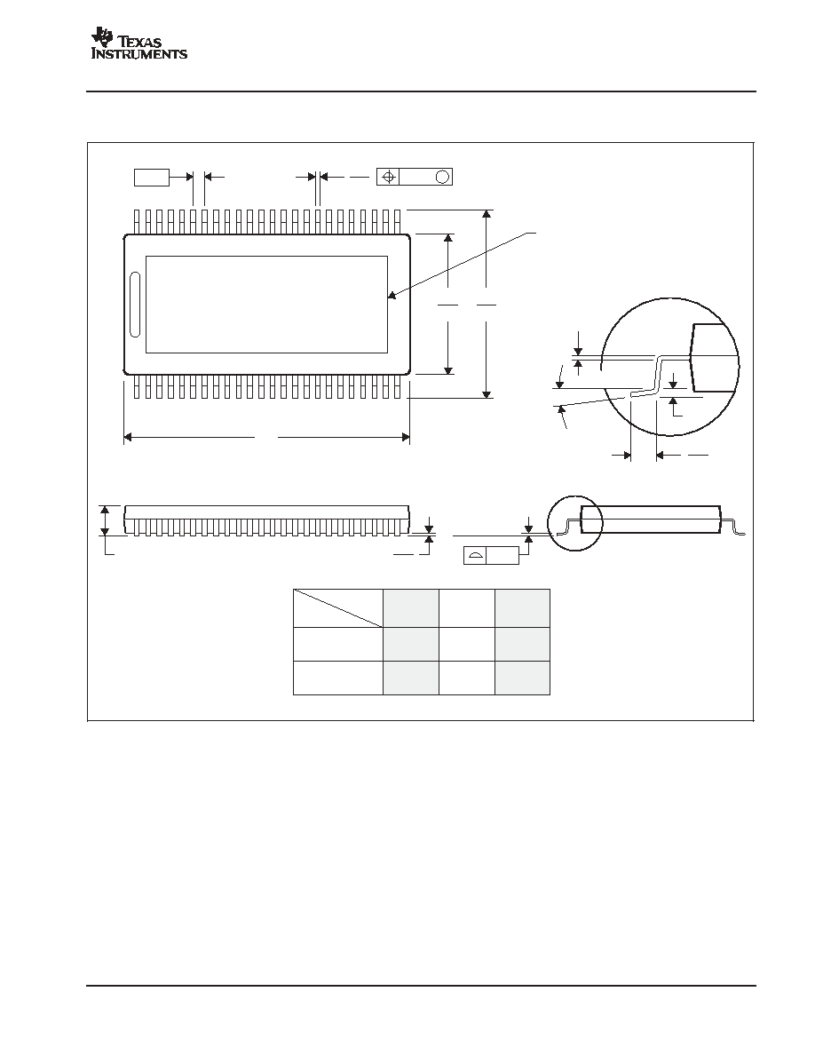
DFD (R-PDSO-G**)
PowerPAD
PLASTIC SMALL-OUTLINE PACKAGE (DIE DOWN)
0,25
0,50
0,75
0,15 NOM
Gage Plane
6,00
6,20
8,30
7,90
Thermal Pad
(See Note D)
64
17,10
56
14,10
Seating Plane
16,90
13,90
4073260/A 02/98
0,27
25
24
A
0,17
48 PINS SHOWN
48
1
48
DIM
PINS **
A MAX
A MIN
1,20 MAX
12,40
12,60
0,10
0,50
M
0,08
0
∞
-8
∞
0,15
0,05
NOTES:A. All linear dimensions are in millimeters.
B. This drawing is subject to change without notice.
C. Body dimensions include mold flash or protrusions.
D. The package thermal performance may be enhanced by attaching an external heatsink to the thermal pad.
This pad is electrically and thermally connected to the backside of the die and possibly selected leads.
E. Falls within JEDEC MO-153
PowerPAD is a trademark of Texas Instruments.

IMPORTANT NOTICE
Texas Instruments Incorporated and its subsidiaries (TI) reserve the right to make corrections, modifications,
enhancements, improvements, and other changes to its products and services at any time and to discontinue
any product or service without notice. Customers should obtain the latest relevant information before placing
orders and should verify that such information is current and complete. All products are sold subject to TI's terms
and conditions of sale supplied at the time of order acknowledgment.
TI warrants performance of its hardware products to the specifications applicable at the time of sale in
accordance with TI's standard warranty. Testing and other quality control techniques are used to the extent TI
deems necessary to support this warranty. Except where mandated by government requirements, testing of all
parameters of each product is not necessarily performed.
TI assumes no liability for applications assistance or customer product design. Customers are responsible for
their products and applications using TI components. To minimize the risks associated with customer products
and applications, customers should provide adequate design and operating safeguards.
TI does not warrant or represent that any license, either express or implied, is granted under any TI patent right,
copyright, mask work right, or other TI intellectual property right relating to any combination, machine, or process
in which TI products or services are used. Information published by TI regarding third-party products or services
does not constitute a license from TI to use such products or services or a warranty or endorsement thereof.
Use of such information may require a license from a third party under the patents or other intellectual property
of the third party, or a license from TI under the patents or other intellectual property of TI.
Reproduction of information in TI data books or data sheets is permissible only if reproduction is without
alteration and is accompanied by all associated warranties, conditions, limitations, and notices. Reproduction
of this information with alteration is an unfair and deceptive business practice. TI is not responsible or liable for
such altered documentation.
Resale of TI products or services with statements different from or beyond the parameters stated by TI for that
product or service voids all express and any implied warranties for the associated TI product or service and
is an unfair and deceptive business practice. TI is not responsible or liable for any such statements.
Following are URLs where you can obtain information on other Texas Instruments products and application
solutions:
Products
Applications
Amplifiers
amplifier.ti.com
Audio
www.ti.com/audio
Data Converters
dataconverter.ti.com
Automotive
www.ti.com/automotive
DSP
dsp.ti.com
Broadband
www.ti.com/broadband
Interface
interface.ti.com
Digital Control
www.ti.com/digitalcontrol
Logic
logic.ti.com
Military
www.ti.com/military
Power Mgmt
power.ti.com
Optical Networking
www.ti.com/opticalnetwork
Microcontrollers
microcontroller.ti.com
Security
www.ti.com/security
Telephony
www.ti.com/telephony
Video & Imaging
www.ti.com/video
Wireless
www.ti.com/wireless
Mailing Address:
Texas Instruments
Post Office Box 655303 Dallas, Texas 75265
Copyright
2003, Texas Instruments Incorporated