 | ÐлекÑÑоннÑй компоненÑ: TC211 | СкаÑаÑÑ:  PDF PDF  ZIP ZIP |
Äîêóìåíòàöèÿ è îïèñàíèÿ www.docs.chipfind.ru
TC211
192-
×
165-PIXEL CCD IMAGE SENSOR
SOCS008B JANUARY 1990
Copyright
©
1990, Texas Instruments Incorporated
2-1
POST OFFICE BOX 655303
·
DALLAS, TEXAS 75265
·
Full-Frame Operation
·
Antiblooming Capability
·
Single-Phase Clocking for Horizontal and
Vertical Transfers
·
Fast Clear Capability
·
Dynamic Range . . . 60 dB Typical
·
High Blue Response
·
High Photoresponse Uniformity
·
Solid-State Reliability With No Image
Burn-In, Residual Imaging, Image
Distortion, Image Lag, or Microphonics
·
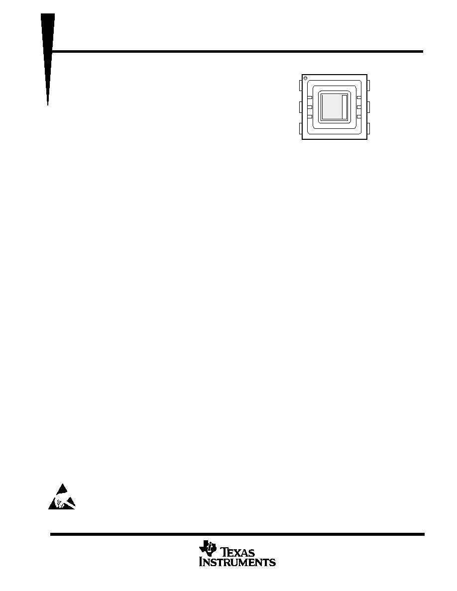
6-Pin Dual-In-Line Ceramic Package
·
Square Image Area:
2640
µ
m by 2640
µ
m
192 Pixels (H) by 165 Pixels (V)
Each Pixel 13.75
µ
m (H) by 16
µ
m (V)
description
The TC211 is a full-frame charge-coupled device (CCD) image sensor designed specifically for industrial
applications requiring ruggedness and small size. The image-sensing area is configured into 165 horizontal
lines each containing 192 pixels. Twelve additional pixels are provided at the end of each line to establish a dark
reference and line clamp. The antiblooming feature is activated by supplying clock pulses to the antiblooming
gate, an integral part of each image-sensing element. The charge is converted to signal voltage at 4
µ
V per
electron by a high-performance structure with built-in automatic reset and a voltage-reference generator. The
signal is further buffered by a low-noise two-stage source-follower amplifier to provide high output-drive
capability.
The TC211 is supplied in a 6-pin dual-in-line ceramic package approximately 7,5 mm (0.3 in.) square. The glass
window can be cleaned using any standard method for cleaning optical assemblies or by wiping the surface with
a cotton swab soaked in alcohol.
The TC211 is characterized for operation from 10
°
C to 45
°
C.
This MOS device contains limited built-in gate protection. During storage or handling, the device leads should be shorted together
or the device should be placed in conductive foam. In a circuit, unused inputs should always be connected to VSS. Under no
circumstances should pin voltages exceed absolute maximum ratings. Avoid shorting OUT to VSS during operation to prevent
damage to the amplifier. The device can also be damaged if the output terminals are reverse-biased and an excessive current is
allowed to flow. Specific guidelines for handling devices of this type are contained in the publication
Guidelines for Handling
Electrostatic-Discharge-Sensitive (ESDS) Devices and Assemblies available from Texas Instruments.
ADB
VSS
ABG
OUT
SRG
IAG
4
5
6
3
2
1
DUAL-IN-LINE PACKAGE
(TOP VIEW)
PRODUCTION DATA information is current as of publication date.
Products conform to specifications per the terms of Texas Instruments
standard warranty. Production processing does not necessarily include
testing of all parameters.
TC211
192-
×
165-PIXEL CCD IMAGE SENSOR
SOCS008B JANUARY 1990
2-2
POST OFFICE BOX 655303
·
DALLAS, TEXAS 75265
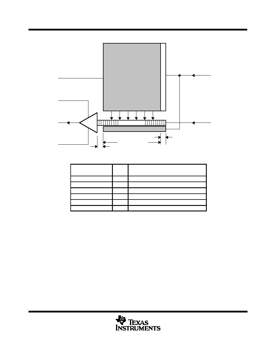
functional block diagram
Serial Register
1
192
Clear Gate
165
12 Dark Pixels
192 Image Pixels
6 Dummy Pixels
ABG
ADB
OUT
VSS
1
3
4
2
6
5
1
IAG
SRG
Terminal Functions
TERMINAL
I/O
DESCRIPTION
NAME
NO.
I/O
DESCRIPTION
ABG
1
I
Antiblooming gate
VSS
2
Amplifier ground
ADB
3
I
Supply voltage for amplifier drain bias
OUT
4
O
Output signal
SRG
5
I
Serial-register gate
IAG
6
I
Image-area gate storage
functional description
The image-sensing area consists of 165 horizontal image lines each containing 192 photosensitive elements
(pixels). Each pixel is 13.75
µ
m (horizontal) by 16.00
µ
m (vertical). As light enters the silicon in the
image-sensing area, free electrons are generated and collected in potential wells (see Figure 1). During this
time, the antiblooming gate is activated by applying a burst of pulses every horizontal blanking interval. This
prevents blooming caused by the spilling of charge from overexposed elements into neighboring elements. The
antiblooming gate is typically held at a midlevel voltage during readout. The quantity of charge collected in each
pixel is a linear function of the incident light and the exposure time. After exposure and under dark conditions,
the charge packets are transferred from the image area to the serial register at the rate of one image line per
each clock pulse applied to the image-area gate. Once an image line has been transferred into the serial register,
the serial-register gate can be clocked until all of the charge packets are moved out of the serial register to the
charge detection node at the amplifier input.
There are 12 dark pixels to the right of the 192 image pixels on each image line. These dark pixels are shielded
from incident light and the signal derived from them can be used to generate a dark reference for restoration
of the video black level on the next image line.
TC211
192-
×
165-PIXEL CCD IMAGE SENSOR
SOCS008B JANUARY 1990
2-3
POST OFFICE BOX 655303
·
DALLAS, TEXAS 75265
functional description (continued)
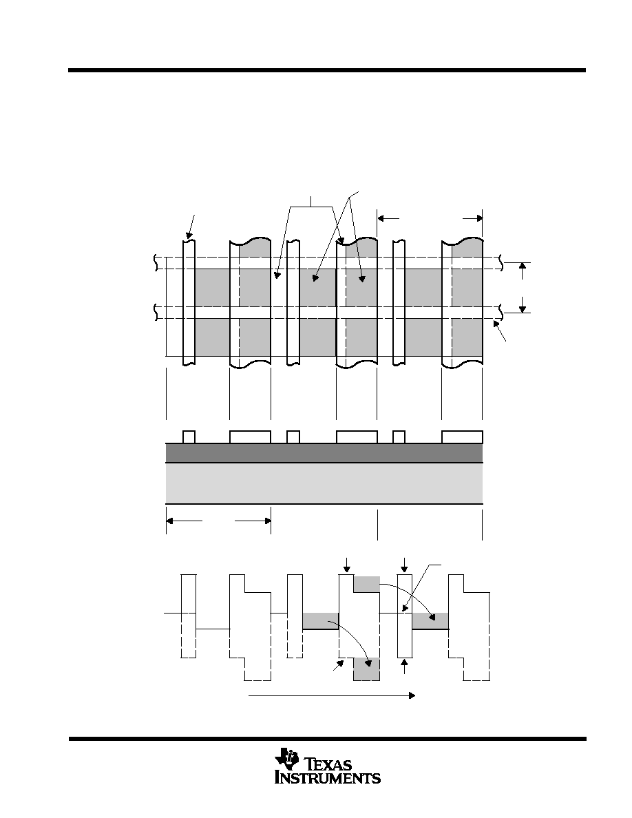
Each clock pulse applied to the image area gate causes an automatic fast clear of the 192 image pixels and
12 dark pixels of the serial register before the next image line is transferred into the serial register. (Note that
the six dummy pixels at the front of the serial register, which are used to transport charge packets from the serial
register to the amplifier input, are not cleared by the image area gate clock.) The automatic fast-clear feature
can be used to initialize the image area by transferring all 165 image lines to the serial register gate under dark
conditions without clocking the serial register gate.
Clocked
Phase
(image-
area
gate)
Virtual
Phase
Virtual
Phase
Virtual
Phase
Antiblooming Gate
Barriers
Potential
Wells
Vertical 16
µ
m
Horizontal
13.75
µ
m
Channel Stop
Representative
Top View of Pixels
1 Pixel
Cross Section
of Pixels
Etched Polysilicon
Insulating Oxide
Silicon
Cross Section
of Potentials
in Silicon
IAG Low
ABG Low
ABG Intermediate
IAG High
ABG High
Direction of Vertical Charge Transfer
Clocked
Phase
(image-
area
gate)
Clocked
Phase
(image-
area
gate)
Figure 1. Charge Accumulation and Transfer Process
TC211
192-
×
165-PIXEL CCD IMAGE SENSOR
SOCS008B JANUARY 1990
2-4
POST OFFICE BOX 655303
·
DALLAS, TEXAS 75265
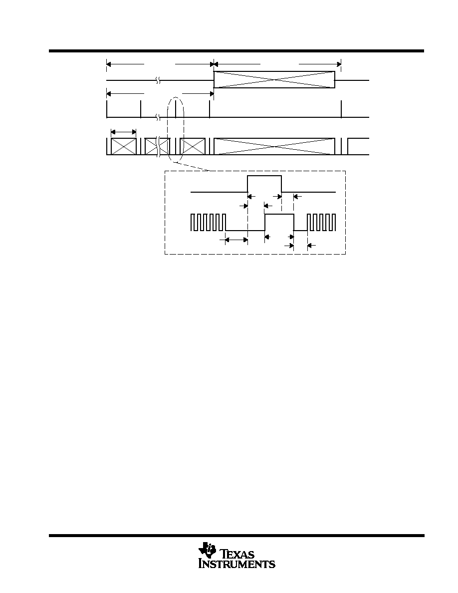
210 Cycles
tw1
t2
t3
t1
tw2
t4
IAG
SRG
Readout
Integration
165 Cycles
ABG
IAG
SRG
Figure 2. Timing Diagram, Noninterlace Mode
absolute maximum ratings over operating free-air temperature range (unless otherwise noted)
Supply voltage range for ADB (see Note 1)
0 V to 15 V
. . . . . . . . . . . . . . . . . . . . . . . . . . . . . . . . . . . . . . . . . . . . . .
Input voltage range for IAG, SRG, ABG, V
I
15 V to 5 V
. . . . . . . . . . . . . . . . . . . . . . . . . . . . . . . . . . . . . . . . . . . . .
Operating free-air temperature range
30
°
C to 85
°
C
. . . . . . . . . . . . . . . . . . . . . . . . . . . . . . . . . . . . . . . . . . . . . . . .
Storage temperature range, T
A
30
°
C to 85
°
C
. . . . . . . . . . . . . . . . . . . . . . . . . . . . . . . . . . . . . . . . . . . . . . . . . . . . .
Lead temperature 1,6 mm (1/16 inch) from case for 10 seconds
260
°
C
. . . . . . . . . . . . . . . . . . . . . . . . . . . . . . .
Stresses beyond those listed under "absolute maximum ratings" may cause permanent damage to the device. These are stress ratings only, and
functional operation of the device at these or any other conditions beyond those indicated under "recommended operating conditions" is not
implied. Exposure to absolute-maximum-rated conditions for extended periods may affect device reliability.
NOTE 1: All voltage values are with respect to VSS.
TC211
192-
×
165-PIXEL CCD IMAGE SENSOR
SOCS008B JANUARY 1990
2-5
POST OFFICE BOX 655303
·
DALLAS, TEXAS 75265
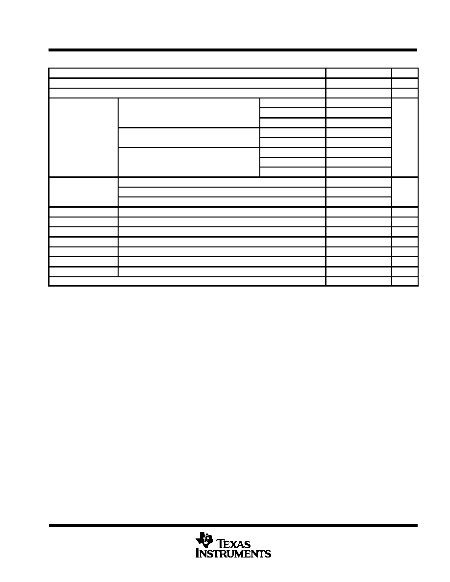
recommended operating conditions
MIN
NOM
MAX
UNIT
Supply voltage, ADB
11
12
13
V
Substrate bias voltage
0
V
High level
1.5
2
2.5
IAG
Intermediate level
10
5
2
Low level
11
10
9
Input voltage V
SRG
High level
1.5
2
2.5
V
Input voltage, VI
SRG
Low level
11
10
9
V
High level
4
4.5
5
ABG
Intermediate level
3
2.5
2
Low level
7.5
7
6.5
IAG
1.5
Clock frequency, fclock
SRG
10
MHz
ABG
2
t1
Time interval, SRG
to IAG
70
ns
t2
Time interval, IAG
to SRG transfer pulse
0
ns
tW1
Pulse duration, IAG high
350
ns
tW2
Pulse duration, SRG transfer pulse high
350
ns
t3
Time interval, IAG
to SRG transfer pulse
350
ns
t4
Time interval, SRG transfer pulse
to SRG clock pulse
70
ns
Capacitive load
OUT
12
pF
Operating free-air temperature, TA
10
45
°
C
The algebraic convention, in which the least-positive (most negative) value is designated minimum, is used in this data sheet for clock voltage
levels.
Adjustment is required for optimal performance.
TC211
192-
×
165-PIXEL CCD IMAGE SENSOR
SOCS008B JANUARY 1990
2-6
POST OFFICE BOX 655303
·
DALLAS, TEXAS 75265
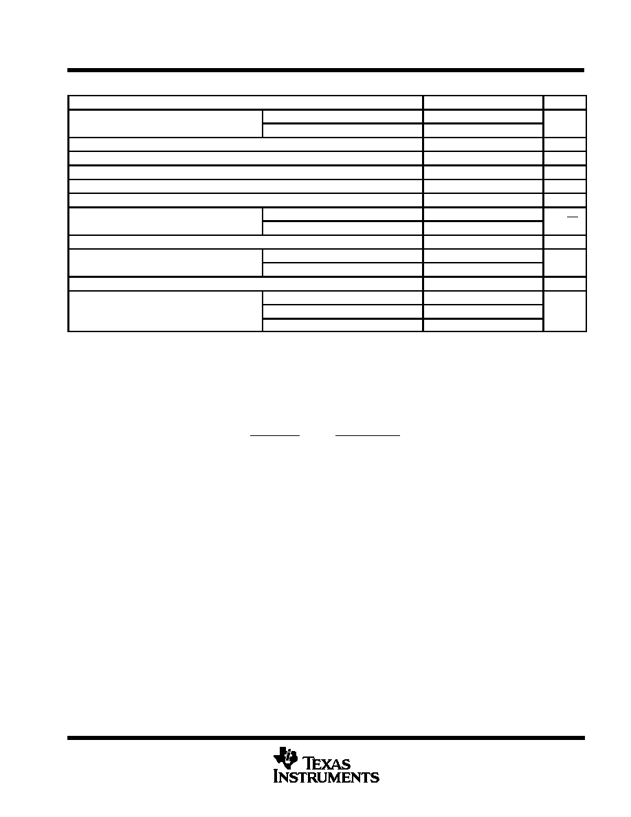
electrical characteristics over recommended operating range of supply voltage, T
A
= 10
°
C to 45
°
C
PARAMETER
MIN
TYP
MAX
UNIT
Dynamic range (see Note 2)
Antiblooming disabled (see Note 3)
60
dB
Dynamic range (see Note 2)
Antiblooming enabled
57
dB
Charge conversion factor
4
µ
V/e
Charge transfer efficiency (see Note 4)
0.99990
0.99998
Signal response delay time,
(see Note 5 and Figure 5)
25
ns
Gamma (see Note 6)
0.97
0.98
0.99
Output resistance
700
800
Noise voltage
1/f noise (5 kHz)
370
nV/
Hz
Noise voltage
Random noise, f = 100 kHz
70
nV/
Hz
Noise equivalent signal
150
electrons
Rejection ratio at 7 16 MHz
From ADB to OUT (see Note 7)
19
dB
Rejection ratio at 7.16 MHz
From SRG to OUT (see Note 8)
37
dB
Supply current
5
10
mA
IAG
1600
Input capacitance, Ci
SRG
25
pF
ABG
780
All typical values are at TA = 25
°
C
NOTES:
2. Dynamic range is 20 times the logarithm of the mean noise signal divided by the saturation output signal.
3. For this test, the antiblooming gate must be biased at the intermediate level.
4. Charge transfer efficiency is one minus the charge loss per transfer in the output register. The test is performed in the dark using
an electrical input signal.
5. Signal response delay time is the time between the falling edge of the SRG clock pulse and the output signal valid state.
6. Gamma (
) is the value of the exponent in the equation below for two points on the linear portion of the transfer function curve (this
value represents points near saturation):
Exposure (2)
Exposure (1)
g
+
Output signal (2)
Output signal (1)
7. ADB rejection ratio is 20 times the logarithm of the ac amplitude at the OUT divided by the ac amplitude at ADB.
8. SRG rejection ratio is 20 times the logarithm of the ac amplitude at the OUT divided by the ac amplitude at SRG.
TC211
192-
×
165-PIXEL CCD IMAGE SENSOR
SOCS008B JANUARY 1990
2-7
POST OFFICE BOX 655303
·
DALLAS, TEXAS 75265
optical characteristics, T
A
= 25
°
C (unless otherwise noted)
PARAMETER
MIN
TYP
MAX
UNIT
Sensitivity (see Note 9)
No IR filter
Measured at VU (see Note 10)
260
mV/lx
Sensitivity (see Note 9)
With IR filter
Measured at VU (see Note 10)
33
mV/lx
Saturation signal (see Note 11)
Antiblooming disabled
400
600
mV
Saturation signal (see Note 11)
Antiblooming enabled
350
450
mV
Blooming overload ratio (see Note 12)
Strobe
5
Blooming overload ratio (see Note 12)
Shuttered light
100
Output signal nonuniformity (1/2 saturation) (see Note 13)
10%
20%
Image-area well capacity
150
×
103
electrons
Dark current
TA = 21
°
C
0.027
nA/cm2
Dark signal (see Note 14)
10
15
mV
Dark signal nonuniformity for entire field (see Note 15)
4
15
mV
Modulation transfer function
Horizontal
50%
Modulation transfer function
Vertical
70%
NOTES:
9. Sensitivity is measured at an integration time of 16.667 ms and a source temperature of 2856 K. A CM-500 filter is used.
10. VU is the output voltage that represents the threshold of operation of antiblooming. VU
1/2 saturation signal.
11. Saturation is the condition in which further increase in exposure does not lead to further increase in output signal.
12. Blooming overload ratio is the ratio of blooming exposure to saturation exposure.
13. Output signal nonuniformity is the ratio of the maximum pixel-to-pixel difference in output signal to the mean output signal for
exposure adjusted to give 1/2 the saturation output signal.
14. Dark-signal level is measured from the dummy pixels.
15. Dark-signal nonuniformity is the maximum pixel-to-pixel difference in a dark condition.
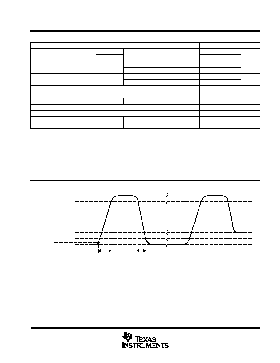
PARAMETER MEASUREMENT INFORMATION
100%
90%
10%
0%
tr
tf
VIH min
VIL max
Intermediate Level
tr = 220 ns, tf = 330 ns for IAG
tr = 115 ns, tf = 135 ns for ABG
Figure 3. Typical Clock Waveform for IAG and ABG
TC211
192-
×
165-PIXEL CCD IMAGE SENSOR
SOCS008B JANUARY 1990
2-8
POST OFFICE BOX 655303
·
DALLAS, TEXAS 75265
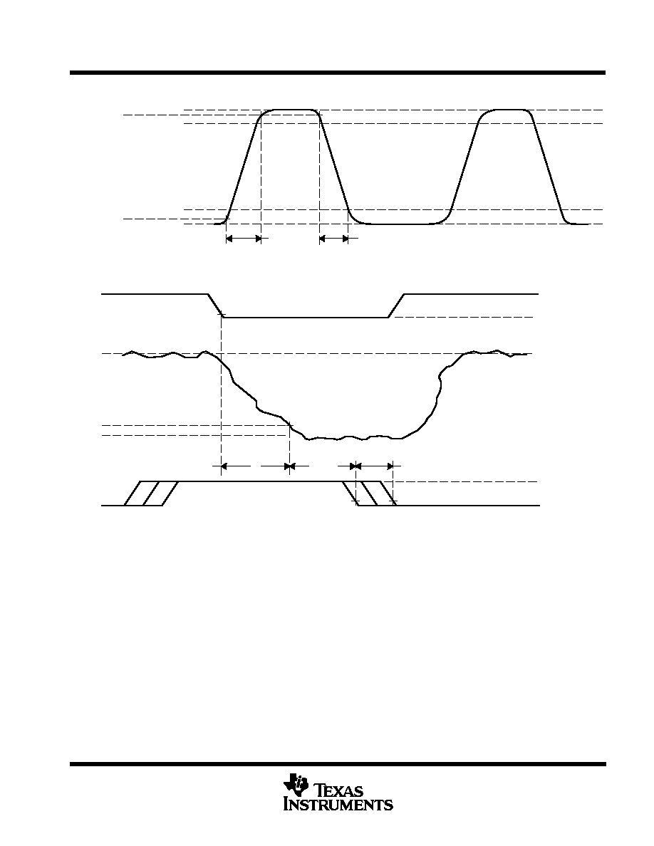
PARAMETER MEASUREMENT INFORMATION
100%
90%
10%
0%
tr
tf
VIH min
VIL max
tr = 25 ns, tf = 30 ns
Figure 4. Typical Clock Waveform for SRG
8.5 V
1.5 V to 2.5 V
8.5 V to 10 V
0%
15 ns
10 ns
t
CCD Delay
SRG
OUT
90%
100%
Sample
and
Hold
Figure 5. SRG and OUT Waveforms
TC211
192-
×
165-PIXEL CCD IMAGE SENSOR
SOCS008B JANUARY 1990
2-9
POST OFFICE BOX 655303
·
DALLAS, TEXAS 75265
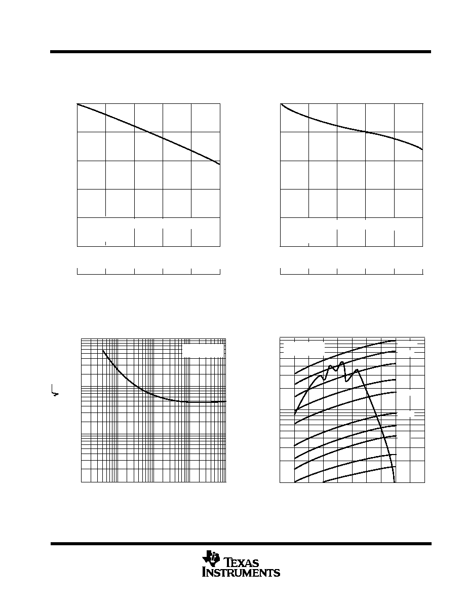
TYPICAL CHARACTERISTICS
VERTICAL MODULATION
TRANSFER FUNCTION
(BARS PARALLEL TO SERIAL REGISTER)
0.4
0.2
0
0
0.2
0.4
0.6
MTF Modulation T
ransfer
Function
0.6
0.8
Normalized Spatial Frequency
1
0.8
1
0
6.3
12.5
18.8
25.0
31.3
Spatial Frequency Cycles/mm
= 400 to 700-nm Monochromatic Light
HORIZONTAL MODULATION
TRANSFER FUNCTION
(BARS PERPENDICULAR TO SERIAL REGISTER)
0.4
0.2
0
0
0.2
0.4
0.6
MTF Modulation T
ransfer
Function
0.6
0.8
Normalized Spatial Frequency
1
0.8
1
0
7.3
14.6
21.8
29.1
36.4
Spatial Frequency Cycles/mm
= 400 to 700-nm Monochromatic Light
VADB = 12 V
TA = 25
°
C
VADB = 12 V
TA = 25
°
C
Figure 6
Figure 7
1
Noise
10
f Frequency Hz
NOISE SPECTRUM OF OUTPUT AMPLIFIER
100
1000
nV/
Hz
103
104
105
106
107
VADB = 12 V
TA = 25
°
C
0.01
1
300
500
700
1100
1300
Responsivity
A/W
Incident Wavelength nm
CCD SPECTRAL RESPONSIVITY
900
0.1
100%
50%
20%
10%
5%
3%
2%
VADB = 12 V
TA = 25
°
C
Figure 8
Figure 9
TC211
192-
×
165-PIXEL CCD IMAGE SENSOR
SOCS008B JANUARY 1990
2-10
POST OFFICE BOX 655303
·
DALLAS, TEXAS 75265
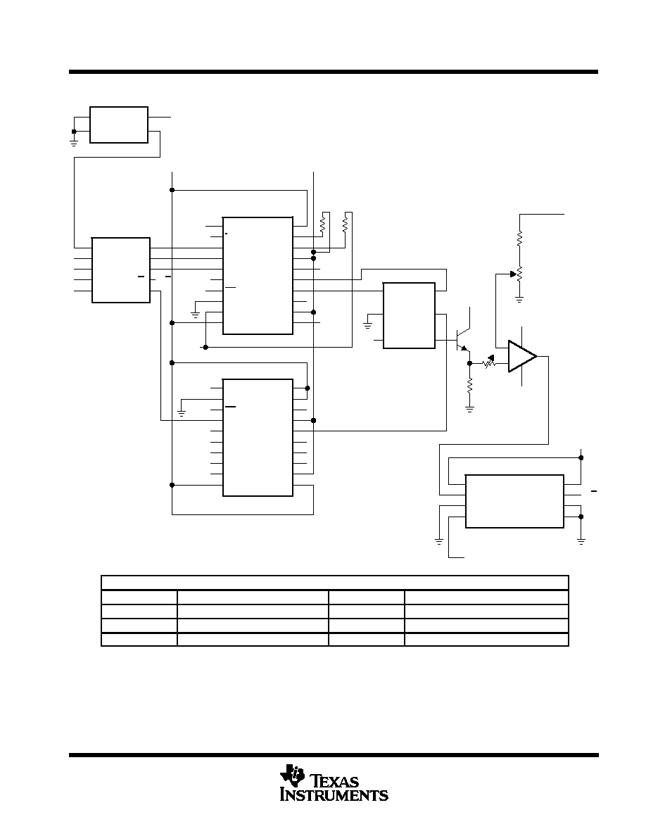
TYPICAL APPLICATION DATA
IALVL
I/N
IAIN
ABIN
MIDSEL
SAIN
PD
GND
VABG+
VSS
VSS
IASR
ABSR
VCC
ABLVL
IAOUT
ABOUT
SAOUT
VCC
VABG
1
2
3
4
5
6
7
8
9
10
20
19
18
17
16
15
14
13
12
11
TMS3473B
SEL0OUT
GND
PD
SRG3IN
SRG2IN
SRG1IN
TRGIN
NC
SEL1OUT
VSS
VSS
SEL0
NC
VCC
SRG3OUT
SRG2OUT
SRG1OUT
TRGOUT
VCC
SEL1
1
2
3
4
5
6
7
8
9
10
20
19
18
17
16
15
14
13
12
11
SN28846
IALVL1
VCC
ABLVL
VABG
VABG+
IAG
ABG
GT1
S/H
SRG
S/H
CLK
CMP
CBNK
CSYNC
TRIG
User-Defined Timer
VCC
GND
CK
GND
1
7
14
8
Master Oscillator
VCC
VSS
VCC
V
47 k
22 k
ABG
VSS
ADB
IAG
SRG
OUT
ADB
1
2
3
6
5
4
ADB
3
2
7
6
4
VDD
ADB
EL2020
2N3904
1 k
500
ADB
2.2 k
5 k
ANLG VCC
ANLG IN
ANLG GND
ANLG OUT
1
2
3
4
DGTL VCC
DGTL IN
DGTL GND
SUB GND
8
7
6
5
VCC
S/H
TL1591
TC211
OUT
Parallel Driver
Serial Driver
Image Sensor
Sample-and-Hold
SUPPORT CIRCUITS
DEVICE
PACKAGE
APPLICATION
FUNCTION
SN28846DW
20 pin small outline
Serial driver
Driver for SRG
TMS3473BDW
20 pin small outline
Parallel driver
Driver for IAG, ABG
TL1591CPS
8 pin small outline (EIAJ)
Sample and hold
Single-channel sample-and-hold IC
Figure 10. Typical Application Circuit Diagram
TC211
192-
×
165-PIXEL CCD IMAGE SENSOR
SOCS008B JANUARY 1990
2-11
POST OFFICE BOX 655303
·
DALLAS, TEXAS 75265
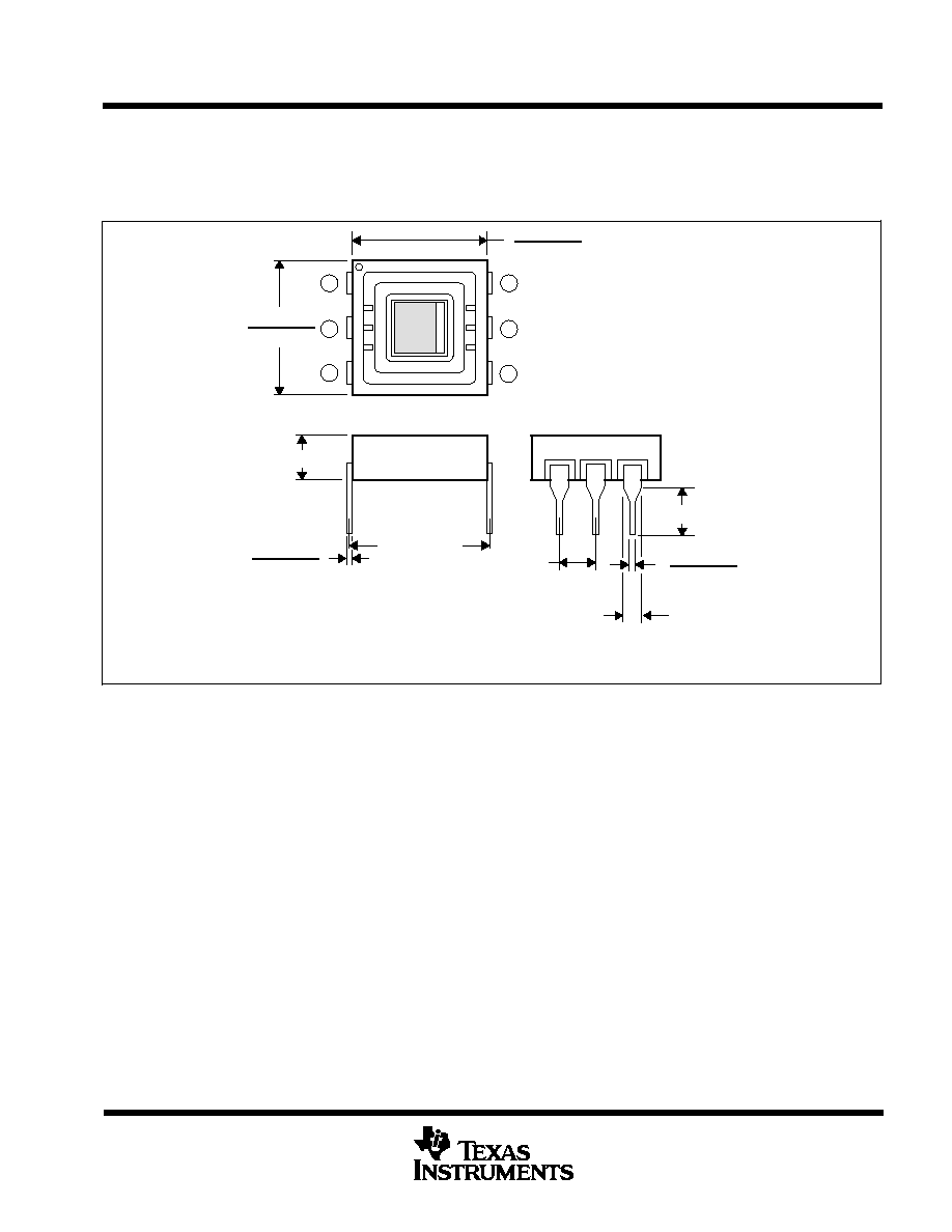
MECHANICAL DATA
The package for the TC211 consists of a ceramic base, glass window, and a 6-lead frame. The glass window is sealed
to the package by an epoxy adhesive. The package leads are configured in a dual-in-line organization and fit into
mounting holes with 2,54 mm (0.1 inch) center-to-center spacings.
4
5
6
3
2
1
2,54 (0.100)
7,62 (0.300)
2,54 (0.100)
7,54 (0.297)
7,14 (0.281)
7,82 (0.308)
7,24 (0.285)
0,31 (0.012)
0,23 (0.009)
0,48 (0.019)
0,38 (0.015)
1,30 (0.051)
1,04 (0.041)
4,45 (0.175)
7/94
NOTES: A. Dimensions are in millimeters and parenthetically in inches. Single dimensions are nominal.
B. The center of the package and the center of the image area are not coincident.
C. The distance from the top of the glass to the image sensor surface is typically 1 mm (0.04 inch). The glass is typically 0.020 inch
thick and has an index of refraction of 1.52.

SOCS008B JANUARY 1990
2-12
POST OFFICE BOX 655303
·
DALLAS, TEXAS 75265

IMPORTANT NOTICE
Texas Instruments and its subsidiaries (TI) reserve the right to make changes to their products or to discontinue
any product or service without notice, and advise customers to obtain the latest version of relevant information
to verify, before placing orders, that information being relied on is current and complete. All products are sold
subject to the terms and conditions of sale supplied at the time of order acknowledgement, including those
pertaining to warranty, patent infringement, and limitation of liability.
TI warrants performance of its semiconductor products to the specifications applicable at the time of sale in
accordance with TI's standard warranty. Testing and other quality control techniques are utilized to the extent
TI deems necessary to support this warranty. Specific testing of all parameters of each device is not necessarily
performed, except those mandated by government requirements.
CERTAIN APPLICATIONS USING SEMICONDUCTOR PRODUCTS MAY INVOLVE POTENTIAL RISKS OF
DEATH, PERSONAL INJURY, OR SEVERE PROPERTY OR ENVIRONMENTAL DAMAGE ("CRITICAL
APPLICATIONS"). TI SEMICONDUCTOR PRODUCTS ARE NOT DESIGNED, AUTHORIZED, OR
WARRANTED TO BE SUITABLE FOR USE IN LIFE-SUPPORT DEVICES OR SYSTEMS OR OTHER
CRITICAL APPLICATIONS. INCLUSION OF TI PRODUCTS IN SUCH APPLICATIONS IS UNDERSTOOD TO
BE FULLY AT THE CUSTOMER'S RISK.
In order to minimize risks associated with the customer's applications, adequate design and operating
safeguards must be provided by the customer to minimize inherent or procedural hazards.
TI assumes no liability for applications assistance or customer product design. TI does not warrant or represent
that any license, either express or implied, is granted under any patent right, copyright, mask work right, or other
intellectual property right of TI covering or relating to any combination, machine, or process in which such
semiconductor products or services might be or are used. TI's publication of information regarding any third
party's products or services does not constitute TI's approval, warranty or endorsement thereof.
Copyright
©
1998, Texas Instruments Incorporated