 | –≠–ª–µ–∫—Ç—Ä–æ–Ω–Ω—ã–π –∫–æ–º–ø–æ–Ω–µ–Ω—Ç: TC245 | –°–∫–∞—á–∞—Ç—å:  PDF PDF  ZIP ZIP |
TC245
786-
◊
488-PIXEL CCD IMAGE SENSOR
SOCS019A ≠ DECEMBER 1991
Copyright
©
1991, Texas Instruments Incorporated
2-1
POST OFFICE BOX 655303
∑
DALLAS, TEXAS 75265
∑
High-Resolution, Solid-State Image Sensor
for NTSC B/W TV Applications
∑
8-mm Image-Area Diagonal, Compatible
With 1/2" Vidicon Optics
∑
755 (H) x 242 (V) Active Elements in
Image-Sensing Area
∑
Advanced On-Chip Signal Processing
∑
Low Dark Current
∑
Electron-Hole Recombination Antiblooming
∑
Dynamic Range . . . More Than 70 dB
∑
High Sensitivity
∑
High Photoresponse Uniformity
∑
High Blue Response
∑
Single-Phase Clocking
∑
Solid-State Reliability With No Image
Burn-in, Residual Imaging, Image
Distortion, Image Lag, or Microphonics
description
The TC245 is a frame-transfer charge-coupled device (CCD) image sensor designed for use in single-chip B/W
NTSC TV applications. The device is intended to replace a 1/2-inch vidicon tube in applications requiring small
size, high reliability, and low cost.
The image-sensing area of the TC245 is configured into 242 lines with 786 elements in each line. Twenty-nine
elements are provided in each line for dark reference. The blooming-protection feature of the sensor is based
on recombining excess charge with charge of opposite polarity in the substrate. This antiblooming is activated
by supplying clocking pulses to the antiblooming gate, which is an integral part of each image-sensing element.
The sensor is designed to operate in an interlace mode, electronically displacing the image-sensing elements
in alternate fields by one-half of a vertical line during the charge integration period, effectively increasing the
vertical resolution and minimizing aliasing. The device can also be operated as a 755 (H) by 242 (V)
noninterlaced sensor with significant reduction in the dark signal.
A gated floating-diffusion detection structure with an automatic reset and voltage reference incorporated on-chip
converts charge to signal voltage. The signal is further processed by a low-noise, state-of-the-art correlated
clamp-sample-and-hold circuit. A low-noise, two-stage, source-follower amplifier buffers the output and
provides high output-drive capability. The image is read out through three outputs, each of which reads out every
third image column.
The TC245 is built using TI-proprietary virtual-phase technology, which provides devices with high blue
response, low dark signal, good uniformity, and single-phase clocking. The TC245 is characterized for operation
from ≠10
∞
C to 45
∞
C.
This MOS device contains limited built-in gate protection. During storage or handling, the device leads should be shorted together
or the device should be placed in conductive foam. In a circuit, unused inputs should always be connected to SUB. Under no
circumstances should pin voltages exceed absolute maximum ratings. Avoid shorting OUTn to ADB during operation to prevent
damage to the amplifier. The device can also be damaged if the output terminals are reverse-biased and an excessive current is
allowed to flow. Specific guidelines for handling devices of this type are contained in the publication
Guidelines for Handling
Electrostatic-Discharge-Sensitive (ESDS) Devices and Assemblies available from Texas Instruments.
SUB 1
IAG 2
ABG 3
ADB 4
OUT3 5
OUT2 6
OUT1 7
AMP GND 8
CDB 9
SUB 10
20 SUB
19 IAG
18 ABG
17 SAG
16 SRG3
15 SRG2
14 SRG1
13 NC
12 TRG
11 IDB
DUAL-IN-LINE PACKAGE
(TOP VIEW)
NC ≠ No internal connection
PRODUCTION DATA information is current as of publication date.
Products conform to specifications per the terms of Texas Instruments
standard warranty. Production processing does not necessarily include
testing of all parameters.
TC245
786-
◊
488-PIXEL CCD IMAGE SENSOR
SOCS019A ≠ DECEMBER 1991
2-2
POST OFFICE BOX 655303
∑
DALLAS, TEXAS 75265
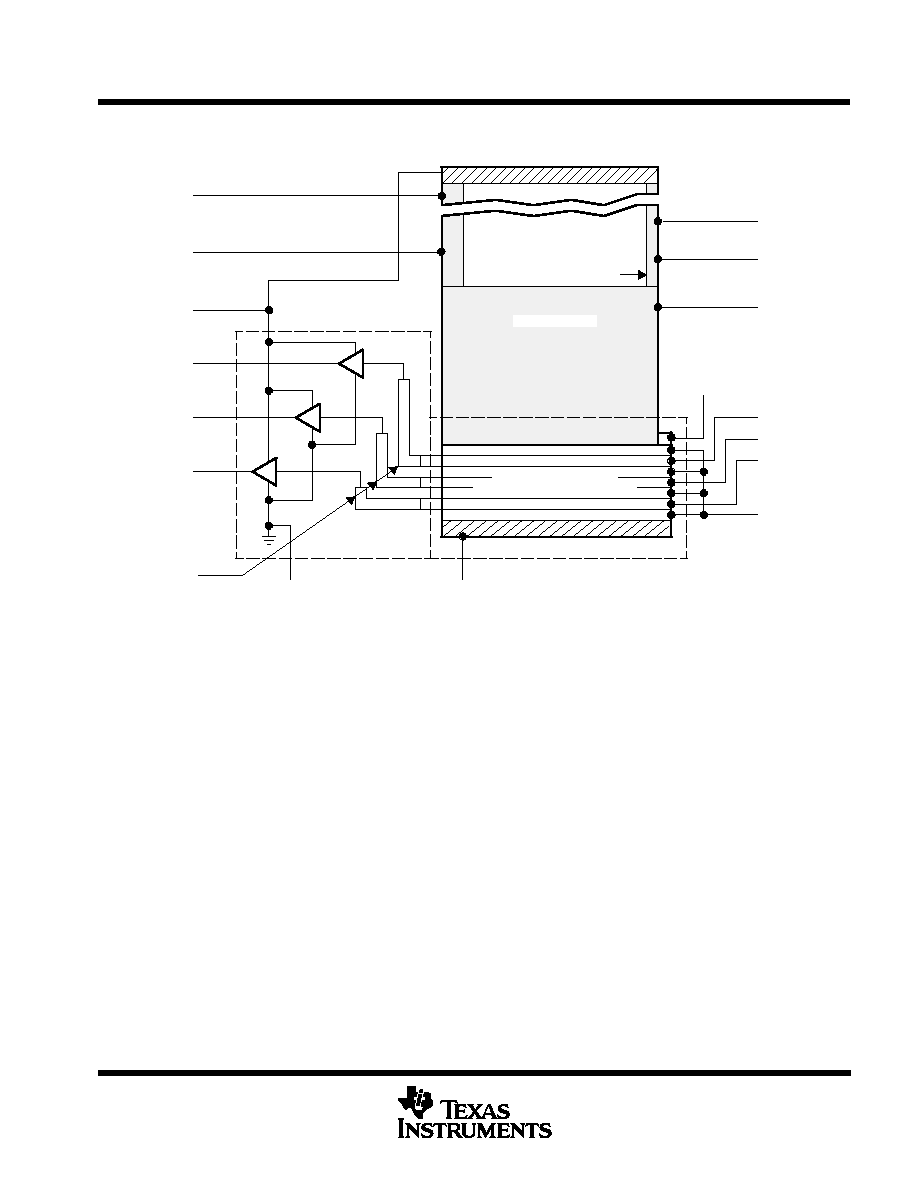
functional block diagram
Dark Reference Elements
Clearing Drain
Amplifiers
OUT2
OUT3
ADB
ABG
IAG
2
3
4
5
6
7
OUT1
8
AMP GND
CDB
9
SRG3
SRG2
SRG1
TRG
IDB
12
14
15
16
SAG
17
ABG
IAG
18
19
Storage Area
Blooming Protection
Image Area With
Top Drain
11 Dummy
Elements
Gates, and Serial Registers
Multiplexer, Transfer
11
detailed description
The TC245 consists of four basic functional blocks: (1) the image-sensing area, (2) the image-storage area,
(3) the multiplexer block with serial registers and transfer gates, and (4) the low-noise signal-processing
amplifier block with charge-detection nodes. The location of each of these blocks is identified in the functional
block diagram.
TC245
786-
◊
488-PIXEL CCD IMAGE SENSOR
SOCS019A ≠ DECEMBER 1991
2-3
POST OFFICE BOX 655303
∑
DALLAS, TEXAS 75265
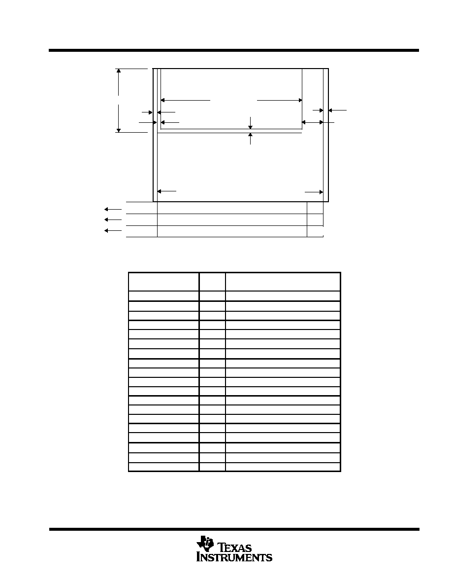
sensor topology diagram
««««««««««««««««««
««««««««««««««««««
««««««««««««««««««
««««««««««««««««««
««««««««««««««««««
««««««««««««««««««
1
1/2
244
755 + 1/2 + 1/2
Effective Imaging Area
1
29 + 1/2
2 Lines
Reverse Transfer
Reverse Transfer
252
252
251 + 1/2 + 1/2
10
10
9.5
11
11
11.5
Dummy Pixels
OPB
Terminal Functions
PIN
I/O
DESCRIPTION
NAME
NO.
I/O
DESCRIPTION
ABG
3
I
Antiblooming gate
ABG
18
I
Antiblooming gate
ADB
4
I
Supply voltage for amplifier drain bias
AMP GND
8
Amplifier ground
CDB
9
I
Supply voltage for clearing drain bias
IAG
2
I
Image-area gate
IAG
19
I
Image-area gate
IDB
11
I
Supply voltage for input diode bias
OUT1
7
O
Output signal 1
OUT2
6
O
Output signal 2
OUT3
5
O
Output signal 3
SAG
17
I
Storage-area gate
SRG1
14
I
Serial-register gate 1
SRG2
15
I
Serial-register gate 2
SRG3
16
I
Serial-register gate 3
SUB
1
Substrate and clock return
SUB
10
Substrate and clock return
SUB
20
Substrate and clock return
TRG
12
I
Transfer gate
All pins of the same name should be connected together externally.

TC245
786-
◊
488-PIXEL CCD IMAGE SENSOR
SOCS019A ≠ DECEMBER 1991
2-4
POST OFFICE BOX 655303
∑
DALLAS, TEXAS 75265
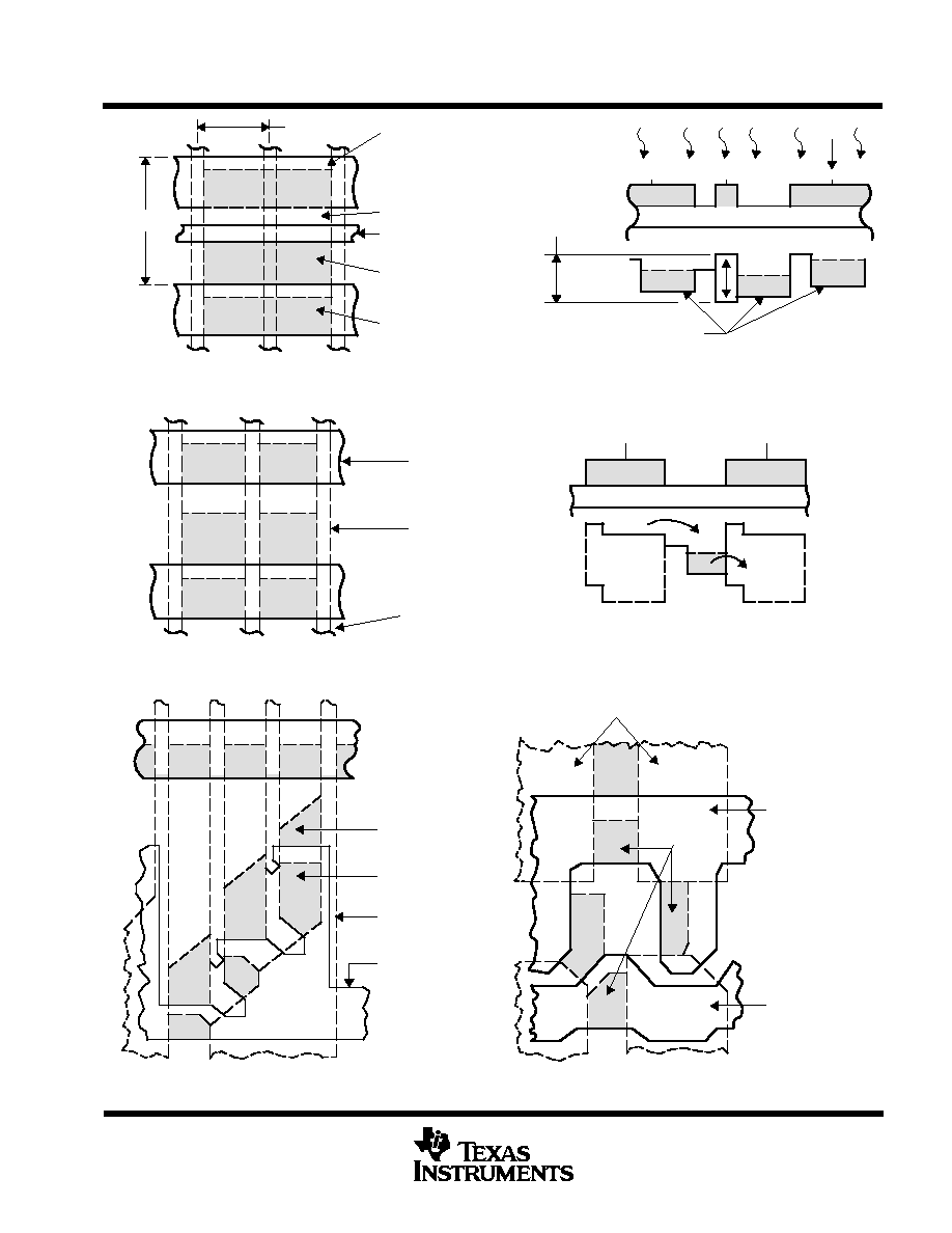
image-sensing and storage areas
Figure 1 and Figure 2 show cross sections with potential well diagrams and top views of image-sensing and
storage-area elements. As light enters the silicon in the image-sensing area, free electrons are generated and
collected in the potential wells of the sensing elements. During this time, blooming protection is activated by
applying a burst of pulses to the antiblooming gate inputs every horizontal blanking interval. This prevents
blooming caused by the spilling of charge from overexposed elements into neighboring elements. After
integration is complete, the signal charge is transferred into the storage area.
There are 29 full columns and one half-column of elements at the right edge of the image-sensing area that are
shielded from incident light; these elements provide the dark reference used in subsequent video processing
circuits to restore the video black level. There are also one full column and one half-column of light-shielded
elements at the left edge of the image-sensing area and two lines of light-shielded elements between the
image-sensing and image-storage areas (the latter prevent charge leakage from the image-sensing area into
the image-storage area).
multiplexer with transfer gates and serial registers
The multiplexer and transfer gates transfer charge line by line from the storage-area columns into the
corresponding serial registers and prepare it for readout. Figure 3 illustrates the layout of the multiplexing gate
that vertically separates the pixels for input into the serial registers. Figure 4 shows the layout of the interface
region between the serial-register gates and the transfer gates. Multiplexing is activated during the horizontal
blanking interval by applying appropriate pulses to the transfer gates and serial registers; the required pulse
timing is shown in Figure 5. A drain is also included to provide the capability to clear the image-sensing and
storage areas of unwanted charge. Such charge can accumulate in the imager during the start-up of operation
or under special circumstances when nonstandard TV operation is desired.
correlated clamp-sample-and-hold amplifier with charge-detection nodes
Figure 6 illustrates the correlated clamp-sample-and-hold amplifier circuit. Charge is converted into a video
signal by transferring the charge onto a floating diffusion structure in detection node1 that is connected to the
gate of MOS transistor Q1. The proportional charge-induced signal is then processed by the circuit shown in
Figure 6. This circuit consists of a low-pass filter formed by Q1 and C2, coupling capacitor C1, dummy detection
node 2, which restores the dc bias on the gate of Q3, sampling transistor Q5, holding capacitor C3, and output
buffer Q6. Transistors Q2, Q4, and Q7 are current sources for each corresponding stage of the amplifier. The
parameters of this high-performance signal-processing amplifier have been optimized to minimize noise and
maximize the video signal.
The signal processing begins with a reset of detection node 1 and restoration of the dc bias on the gate of Q3
through the clamping function of dummy detection node 2. After the clamping is completed, the new charge
packet is transferred onto detection node 1. The resulting signal is sampled by the sampling transistor Q5 and
is stored on the holding capacitor C3. This process is repeated periodically and is correlated to the charge
transfer in the registers. The correlation is achieved automatically since the same clock lines used in registers
-S2 and
-S3 for charge transport serve for reset and sample. The multiple use of the clock lines significantly
reduces the number of signals required to operate the sensor. The amplifier also contains an internal voltage
reference generator that provides the reference bias for the reset and clamp transistors. The detection nodes
and the corresponding amplifiers are located some distance away from the edge of the storage area. Therefore,
eleven dummy elements are incorporated at the end of each serial register to span the distance. The location
of the dummy elements, which are considered to be part of the amplifiers, is shown in the functional block
diagram.
TC245
786-
◊
488-PIXEL CCD IMAGE SENSOR
SOCS019A ≠ DECEMBER 1991
2-5
POST OFFICE BOX 655303
∑
DALLAS, TEXAS 75265
-ABG
-IAG
8.5
µ
m(H)
Clocked Barrier
Virtual Barrier
Antiblooming Gate
Virtual Well
Clocked Well
Light
Antiblooming
Clocking Levels
Accumulated Charge
19.75
µ
m(V)
Figure 1. Charge-Accumulation Process
-PS
Channel Stops
Virtual Phase
Clocked Phase
Figure 2. Charge-Transfer Process
Gate
Multiplexing
Stop
Channel
Well
Clocked
Well
Virtual
Gate
Transfer
Serial-Register
Gate
Wells
Clocked
Channel Stops
Figure 3. Multiplexing-Gate Layout
Figure 4. Interface-Region Layout