
GENERAL DESCRIPTION
TLSI's family of Video Circuits is ideally suited for
a wide range of applications in which cost, size,
power and the number of discrete components
need to be minimized. T310 ICs bring modern
functionality to video applications requiring text or
graphics insertion. The analog transparent mode
modulates the video with the text or graphics input
so the video is not totally obscured. The resulting
video is adjustable in contrast and level so a flexible
range of overlays is possible. YUV inputs are
accommodated using an external black level key.
FEATURES
∑
Transparent Mode
∑
Programmable Gain and Offset
∑
RGB/YUV Inputs
∑
Supply Voltage 3.0V to 5.5V
∑
Operating Temperature -40∞C to +85∞C
∑
Power Less than 250 mW
∑
Applications: TVs, set-top boxes,
VCRs, Personal Video Recording
and Internet TV
T 3 1 0
O n S c re e n D i s p l a y M i x e r
P
R
E
L
I
M
I
N
A
R
Y
BLOCK DIAGRAM
CONTROL
LOGIC
VIDEO MIXER
GRAPHICS/
TEXT
PROCESSOR
BLACK
LEVEL
CLAMP
ANALOG/DIGITAL
TEXT/GRAPHICS INPUT
R
G
B
BLACK
LEVEL KEY
BLACK
LEVEL
CLAMP
BLACK
LEVEL
CLAMP
BLACK
LEVEL
CLAMP
BLACK
LEVEL
CLAMP
BLACK
LEVEL
CLAMP
R IN
G IN
B IN
FAST ENABLE GAIN OFFSET
R OUT
G OUT
B OUT
PARAMETER CONDITIONS
UNITS
Supply Voltage
V
SS
- 0.5
V
DD
5.5 V
DC Input Voltage
V
SS
- 0.5
V
IN
V
DD
+ 0.5
V
DC Output Voltage
V
SS
- 0.5
V
OUT
V
DD
+ 0.5
V
Storage Temperature
-65 < T
S
< +150
∞C
Ambient Temperature -40 < T
A
< +85
∞C
Junction Temperature
-65 < T
J
< +125
∞C
Soldering Temperature
T
SLDR
< 260 for less than 10 seconds
∞C
ABSOLUTE MAXIMUM RATINGS*
* Operation of the device at or beyond these specifications may result in permanent damage or
affect operation and reliability of the product.
PARAMETER CONDITIONS
SYMBOL
MIN
TYP
MAX
UNITS
Supply Voltage
V
DD
4.5 5.0 5.5 V
High-Level Control Input Voltage
V
I H
4.0 V
Low-Level Control Input Voltage
V
I L
1.0
V
Fast Enable
I
I H
1.0 µA
Fast Enable
I
I L
-10.0
µA
Supply Current
C
L
=5pF
I
DD
25.0 mA
Output Black Level
1.0
V
Input Bias Current
15.0
µA
Short-Circuit Output Source Current
< 20 seconds
I
OS H
-20.0
mA
Short-Circuit Sink Current
< 20 seconds
I
OS L
20.0 mA
ELECTRICAL CHARACTERISTICS
DC CHARACTERISTICS
V
DD
= 5.0V, -40∞C < T
A
< +85∞C unless otherwise specified
2
AC CHARACTERISTICS
V
DD
= 5.0V, -40∞C < T
A
< +85∞C unless otherwise specified
PARAMETER CONDITIONS
SYMBOL
MIN
TYP
MAX
UNITS
RGB/YUV Input Level
V
I N
1
V
P P
RGB/YUV Output Level
Load=1000 ohms
V
OUT
2
V
P P
RGB/YUV Output Level
Load=75 ohms
V
OUT
1
V
P P
(see test circuit)
Bandwidth
BW
50
MHz
Fast Enable Switching Time
10
nS
Output Rise and Fall Time
C
L
=5pF
t
r
,t
f
7
nS
Input Capacitance
1.5
pF
3
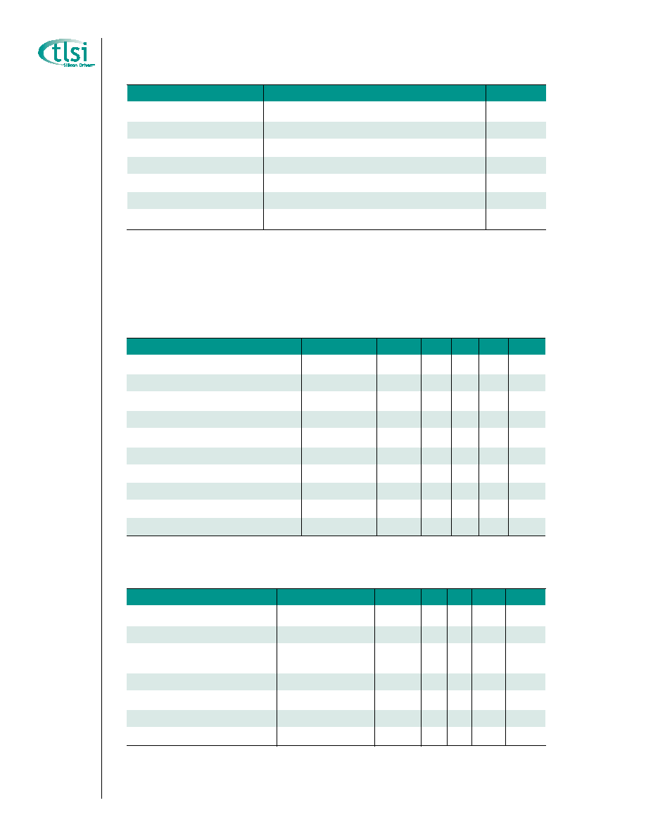
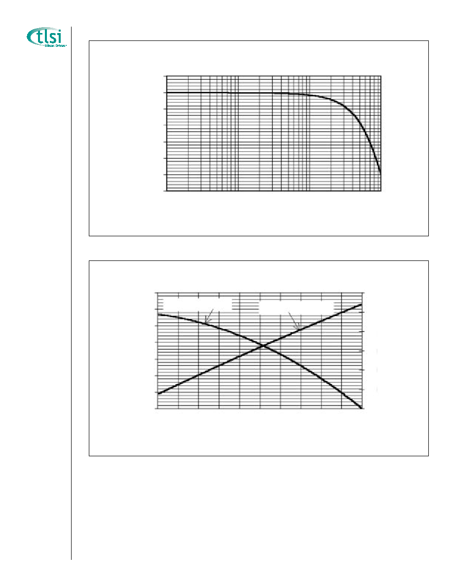
GRAPHS OF TYPICAL OPERATING CONDITIONS
1
1 1.2 1.4 1.6 1.8 2
0.01
0
-0.01
-0.02
-0.03
-0.04
-0.05
-0.06
0.06
0.05
0.04
0.03
0.02
0.01
0
20
0
-20
-40
-60
-80
-100
-120
10
Frequency, MHz
DC Voltage
Magnitude, dB
Dif
fer
ential Gain, per
cent
Dif
fer
ential Phase, degr
ees
100
1000
Frequency Response, T = 25∞C
Differential Gain and Phase, 3.58 MHz
Differential Gain
Differential Phase

4
TEST CIRCUIT SCHEMATIC
Pin number assignments are subject to change.
TRANSPARENT VIDEO
RED IN
T310
GAIN
OFFSET
VSUPPLY
5V
FAST
ENABLE
+
+
-
-
+
-
GREEN IN
BLUE IN
75
75
75
RED OUT
BLUE OSD IN
GREEN OSD IN
RED OSD IN
GREEN OUT
BLUE OUT
75
75
75
0.1
µF
0.1
µF
0.1
µF
75
13.7 MHz
75
75
75
75
75
1
2
3
4
5
6
7
8
16
15
14
13
12
11
10
9
R/Y_IN
G/U_IN
B/V_IN
NC
GAIN
OFST
BLK
VEE
ROSD
GOSD
BOSD
FEN
ROUT
GOUT
BOUT
VCC
T310 TEST CIRCUIT
V
V
V
Text transparency can be varied to suit the application.
