November 2002
This document contains information on a preproduction product. Specifications and information herein are subject to change without notice.
11.5.02
T83027
PLL Clock Generator IC with VCXO
ISO9001
1.0 Features
∑
Phase-Locked Loop (PLL) device synthesizes output
clock frequency from crystal or external reference
clock
∑
One-chip tunable voltage controlled crystal oscillator
(VCXO) allows precise system frequency tuning
∑
3.3V operation
∑
8 pin (150 mil) SOIC package
∑
Uses inexpensive 14pF pullable crystals with no
external capacitors required.
∑
12mA drive capability at TTL levels
∑
Very low phase noise PLL
2.0 Applications
∑
Set-top boxes
∑
MPEG Video clock source
∑
Oscillator replacement
3.0 Description
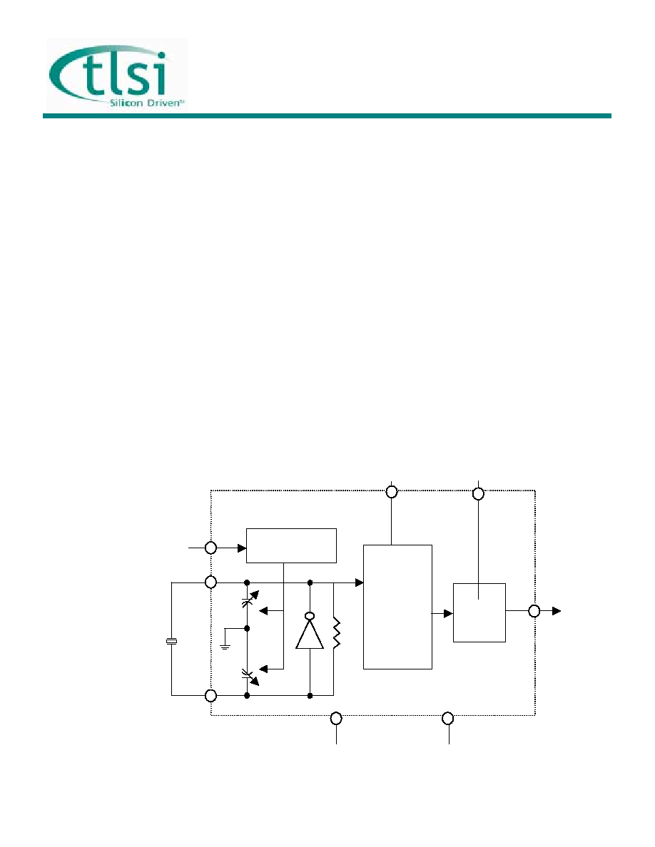
The T83027 is a single-chip, low-jitter Voltage-Controlled-
Crystal-Oscillator combined with a low noise Phase
Locked Loop. The device accepts a 13.5 MHz, 14 pF
crystal, and produces a low jitter 27 MHz output
frequency. A 0 to 3.0V control signal is used to fine tune
the output clock frequency in the ±100ppm range. This
finds use in systems that have frequency matching
requirements, such as digital satellite receivers.
Figure 1: Block Diagram
CLK
VDD2
VDD1
X2
Load Cap Control
Output
Buffer
Load
Caps
13.5 MHz
Pullable
Crystal
VIN
X1
GND1
GND2
Low
Phase
Noise
PLL

November 2002
2
11.5.02
ISO9001
T83027
PLL Clock Generator IC with VCXO
Table 1: Pin Descriptions
PIN TYPE NAME
DESCRIPTION
1
Xi
X1
Crystal Connection. Connect to a 13.5 MHz Pullable Crystal or reference
frequency input.
2 P
VDD1
Core
V
DD
. Connect to 3.3V
3
I
VIN
Voltage input to VCXO. Zero to 3V Signal Controls the Frequency of the
VCXO.
4
P
GND2
Connect to Ground.
5
O
CLK
Clock Output
6
P
VDD2
Pad Driver V
DD
. Connect to 3.3V
7
P
GND1
Connect to Ground.
8
Xi
X2
Crystal Connection. Connect to a 13.5 MHz pullable crystal.
Legend: I = Input
O = Output
P = Power supply connection
Xi = Crystal connections.
1
2
3
4
8
7
6
5
X1
VDD1
VIN
GND2
X2
GND1
VDD2
CLK
8-pin (150 mil) SOIC

November 2002
3
11.5.02
ISO9001
T83027
PLL Clock Generator IC with VCXO
T83027 Typical Deviation vs. Vin
13.5 MHz 14pF Crystal
-150
-100
-50
0
50
100
150
0.000
0.500
1.000
1.500
2.000
2.500
3.000
Vin
Deviation From 27 MHz in PPM
4.0 Functional Block Description
4.1
Voltage Controlled Crystal Oscillator
The VCXO provides a tunable, low-jitter frequency reference. Loading capacitance for the crystal is internal to the
T83027. No external components (other than the crystal resonator itself) are required for operation of the VCXO.
Tuning of the VCXO frequency is accomplished by varying the voltage on Vin (Pin 3).
The oscillator operates the crystal resonator in the parallel-resonant mode. Crystal warping, or the "pulling" of the
crystal oscillation frequency, is accomplished by altering the effective load capacitance presented to the crystal by the
oscillator circuit. The actual amount that changing the load capacitance alters the oscillator frequency will be
dependent on the characteristics of the crystal as well as the
oscillator circuit itself.
Specifically, the motional capacitance of the crystal (usually
referred to by crystal manufacturers as C
1
), the static
capacitance of the crystal (C
0
), and the load capacitance
(C
L
) of the oscillator determine the "warping" or "pulling"
capability of the crystal in the oscillator circuit. A simple
formula to obtain the warping capability of a crystal oscillator
is:
(
)
(
) (
)
C
C
C
C
C
C
C
ppm
f
L
L
L
L
1
0
2
0
6
1
2
1
2
10
)
(
+
◊
+
◊
◊
-
◊
=
where C
L1
and C
L2
are the two extremes of the applied load
capacitance.
EXAMPLE: A crystal with the following parameters is used.
With C
1
= 0.025pF, C
0
= 6pF, C
L1
= 10pF, and C
L2
= 20pF,
the tuning range is
(
)
(
) (
)
ppm
.
f
300
10
6
20
6
2
106
10
20
025
0
=
+
◊
+
◊
◊
-
◊
=
.
4.2
Phase Locked Loop (PLL)
The on-chip PLL is a standard phase locked loop architecture that multiplies the reference frequency by two. The
frequency multiplication is exact with zero synthesis error.

November 2002
4
11.5.02
ISO9001
T83027
PLL Clock Generator IC with VCXO
5.0 Electrical
Specifications
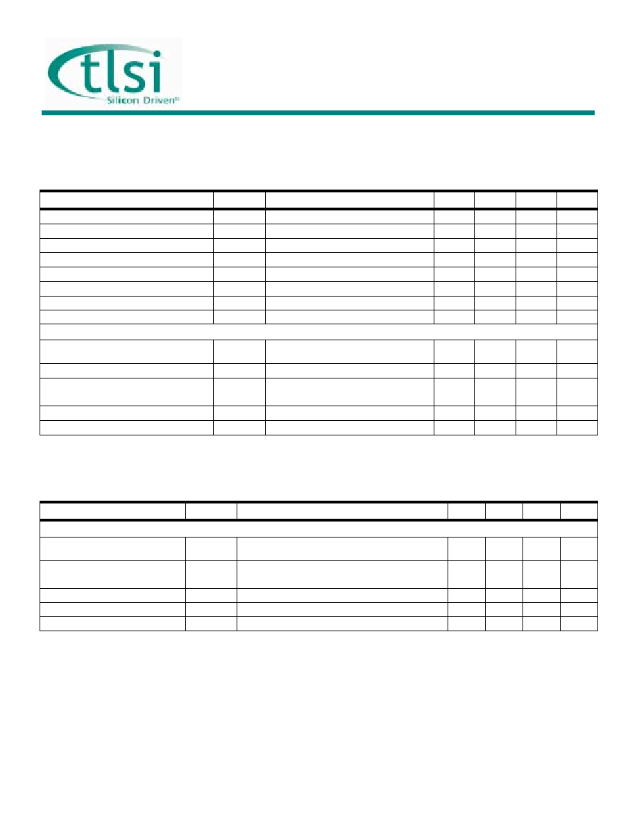
Table 2: Absolute Maximum Ratings
Stresses above those listed under Absolute Maximum Ratings may cause permanent damage to the device. These conditions represent a stress rating only, and functional operation of the device at
these or any other conditions above the operational limits noted in this specification is not implied. Exposure to maximum rating conditions for extended conditions may affect device performance,
functionality, and reliability.
PARAMETER SYMBOL
MIN.
MAX.
UNITS
Supply Voltage (V
SS
= ground)
V
DD
V
SS
-0.5 5
V
Input Voltage, dc
V
I
V
SS
-0.5 V
DD
+0.5 V
Output Voltage, dc
V
O
V
SS
-0.5 V
DD
+0.5 V
Input Clamp Current, dc (V
I
< 0 or V
I
> V
DD
) I
IK
-25 25 mA
Output Clamp Current, dc (V
I
< 0 or V
I
> V
DD
) I
OK
-50 50 mA
Storage Temperature Range (non-condensing)
T
S
-65 150 ∞C
Ambient Temperature Range, Under Bias
T
A
-55 125 ∞C
Junction Temperature
T
J
125
∞C
Lead Temperature (soldering, 10s)
260
∞C
Input Static Discharge Voltage Protection
2
KV
Table 3: Operating Conditions
PARAMETER SYMBOL
CONDITIONS/DESCRIPTION
MIN.
TYP.
MAX.
UNITS
Core Supply Voltage (V
DD
) V
DD
3.15 3.3 3.45 V
VCXO Control Voltage, V
IN
V
IN
0
V
DD
V
Ambient Operating Temperature Range
T
A
0
70 ∞C
Crystal Resonator Frequency
f
XTAL
Fundamental
Mode
12 13.5 20 MHz
November 2002
5
11.5.02
ISO9001
T83027
PLL Clock Generator IC with VCXO
Table 4: DC Electrical Specifications
Unless otherwise stated, V
DD
= 3.15V to 3.45V , no load on any output, and ambient temperature range T
A
= 0∞C to 70∞C.
PARAMETER SYMBOL
CONDITIONS/DESCRIPTION
MIN.
TYP.
MAX.
UNITS
Supply Current, Dynamic, with no load
I
DD
f
XTAL
= 13.5MHz No Load
28
mA
Output High Voltage
V
OH
I
OH
= -12mA
2.4
V
Output Low Voltage
V
OL
I
OL
= 12mA
0.4
V
Input Low Current
I
IL
0 Volts X1 (Pin 1) and VIN (Pin 3) Inputs
-60
µ
A
Input High Current
I
IH
3 Volts X1 (Pin 1) and VIN (Pin 3) Inputs
60
µ
A
Short Circuit Current
I
OS
Clock Output (Pin 5)
±
85
mA
Input Low Voltage
V
IL
X1 (Pin 1) being Driven
0.4
V
Input High Voltage
V
IH
X1 (Pin 1) being Driven
2.5
Voltage Controlled Crystal Oscillator - VDD=3.3V
Crystal Loading Capacitance
C
L(xtal)
As seen by a crystal connected to XIN and
XOUT (@ V
XTUNE
= 1.65V)
14 pF
Crystal Gamma
C
O
/C
1
240
VCXO Tuning Range
f
XTAL
= 13.5 MHz; C
L(xtal)
= 14pF
gamma = 240; (peak-to peak)
200 250 ppm
VCXO Tuning Characteristic
Note: positive
F for positive
V
75
ppm/V
Crystal ESR
35
Table 5: AC Timing Specifications
Unless otherwise stated, V
DD
= 3.15V to 3.45V, no load on any output, and ambient temperature range T
A
= 0∞C to 70∞C. Parameters denoted with an asterisk ( * ) represent nominal characterization
data and are not production tested to any specific limits.
PARAMETER SYMBOL CONDITIONS/DESCRIPTION MIN.
TYP.
MAX.
UNITS
Clock Output (CLK)
Duty Cycle *
Ratio of high pulse width (as measured from rising
edge to next falling edge at V
DD
/2) to one clock period
40 60 %
Jitter, Period (peak-peak) *
t
j(
P)
From rising edge to next rising edge at V
DD
/2,
C
L
= 10pF; f
XTAL
= 13.5 MHz
±
70
ps
Phase Noise
f
XTAL
= 13.5 MHz: Offset Frequency = 100KHz
-100
dBc
Rise Time *
t
r
Measured 0.8V to 2.0V, C
L
= 10pF
1.5
ns
Fall Time *
t
f
Measured 2.0V to 0.8V; C
L
= 10pF
1.5
ns