 | –≠–ª–µ–∫—Ç—Ä–æ–Ω–Ω—ã–π –∫–æ–º–ø–æ–Ω–µ–Ω—Ç: T224160B | –°–∫–∞—á–∞—Ç—å:  PDF PDF  ZIP ZIP |
TE
CH
tm
T224160B
Taiwan Memory Technology, Inc. reserves the right
P. 1
Publication Date: MAR. 2001
to change products or specifications without notice.
Revision:B
DRAM
256K x 16 DYNAMIC RAM
FAST PAGE MODE
FEATURES
∑
Industry-standard x 16 pinouts and timing
functions.
∑
Single 5V (
±
10%) power supply.
∑
All device pins are TTL- compatible.
∑
512-cycle refresh in 8ms.
∑
Refresh modes: RAS only, CAS BEFORE
RAS (CBR) and HIDDEN.
∑
Conventional FAST PAGE MODE access cycle.
∑
BYTE WRITE and BYTE READ access
cycles.
OPTION
TIMING
MARKING
30ns
-30
35ns
-35
45ns
-45
60ns
-60
PACKAGE
MARKING
SOJ J
TSOP(II) S
GENERAL DESCRIPTION
The T224160B is a randomly accessed solid state
memory containing 4,194,304 bits organized in a x16
configuration. The T224160B has both BYTE
WRITE and WORD WRITE access cycles via two
CAS pins. It offers Fast Page mode operation
The T224160B CAS function and timing are
determined by the first CAS to transition low and
by the last to transition back high. Use only one of
the two
CAS
and leave the other staying high during
WRITE will result in a BYTE WRITE. CASL
transiting low in a WRITE cycle will write data into
the lower byte (IO1~IO8), and CASH transiting low
will write data into the upper byte (IO9~16).
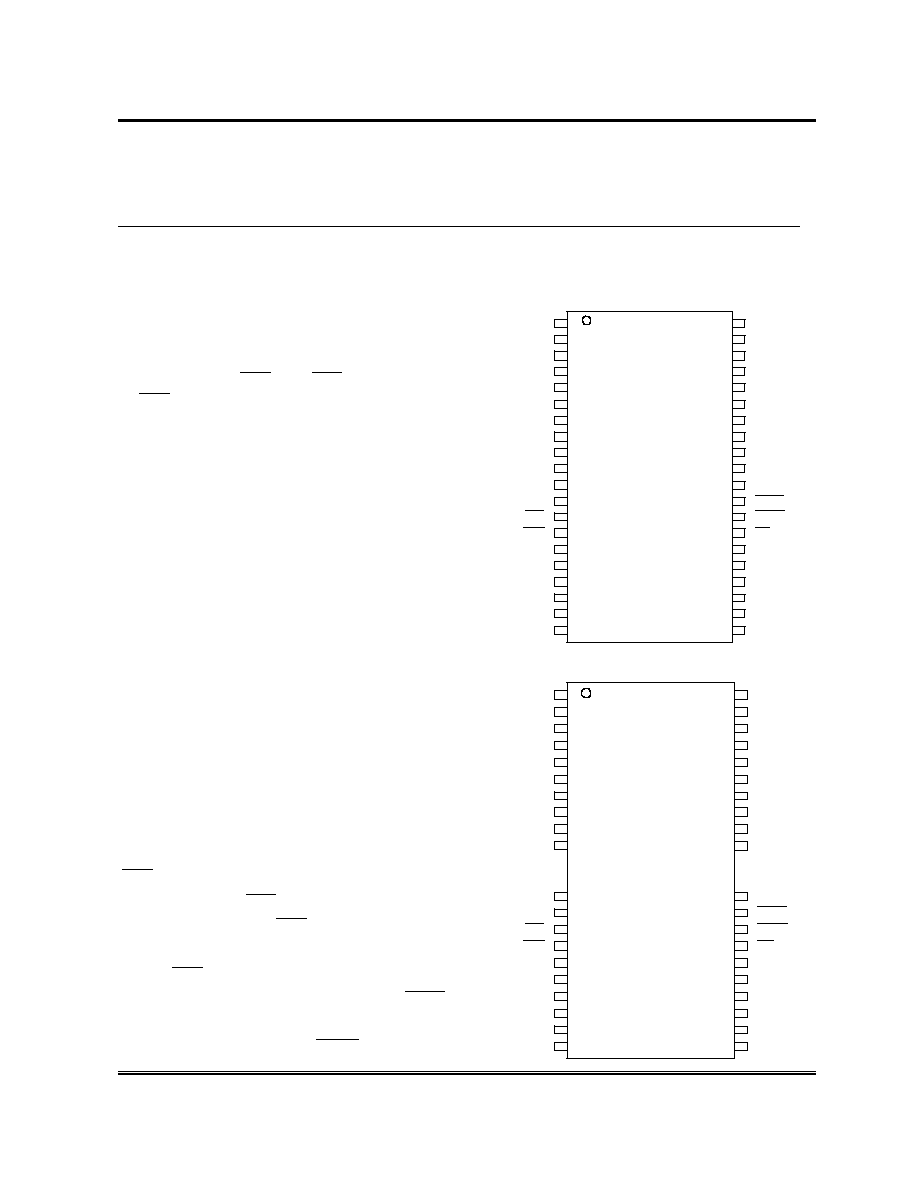
PIN ASSIGNMENT ( Top View )
I/01
Vcc
I/02
I/03
I/04
I/05
Vcc
I/06
I/07
I/08
NC
NC
NC
A0
A1
Vcc
A2
A3
WE
RAS
40
39
38
37
35
36
34
33
32
31
30
29
28
27
26
25
24
23
22
21
1
2
3
4
6
5
7
8
9
10
11
12
13
14
15
16
17
18
19
20
I/016
Vss
I/015
I/014
I/013
I/012
Vss
I/011
I/010
I/09
NC
A8
A7
A6
VSS
A5
A4
CASL
CASH
OE
SOJ
I/01
Vcc
I/02
I/03
I/04
I/05
Vcc
I/06
I/07
I/08
NC
NC
NC
A0
A1
Vcc
A2
A3
WE
RAS
40
39
38
37
35
36
34
33
32
31
30
29
28
27
26
25
24
23
22
21
1
2
3
4
6
5
7
8
9
10
11
12
13
14
15
16
17
18
19
20
I/016
Vss
I/015
I/014
I/013
I/012
Vss
I/011
I/010
I/09
NC
A8
A7
A6
VSS
A5
A4
CASL
CASH
OE
TSOP(II)

TE
CH
tm
T224160B
Taiwan Memory Technology, Inc. reserves the right
P. 2
Publication Date: MAR. 2001
to change products or specifications without notice.
Revision:B
FUNCTIONAL BLOCK DIAGRAM
NO.2 CLOCK
GENERATOR
COLUMN.
ADDRESS
BUFFER
REFRESH
CONTROLLER
REFRESH
COUNTER
ROW.
ADDRESS
BUFFERS(9)
NO.1 CLOCK
GENERATOR
CONTROL
LOGIC
DATA-IN BUFFER
DATA-OUT
BUFFER
COLUMN
DECODER
ROW
DECODER
512 x 512 x 16
MEMORY
ARRAY
SENSE AMPLIFIERS
VO GATING
16
512 x 16
512
A0
A1
A2
A3
A4
A5
A6
A7
A8
512
RAS
CAS
DQ01
.
.
DQ16
OE
16
8
8
9
9
9
9
9
CASH
CASL
WE
Vcc
Vss
PIN DESCRIPTIONS
PIN NO.
SYM.
TYPE
DESCRIPTION
16~19,22~26
A0-A8
Input
Address Input
14
RAS
Input
Row Address Strobe
28
CASH
Input
Column Address Strobe /Upper Byte Control
29
CASL
Input
Column Address Strobe /Lower Byte Control
13
WE
Input
Write Enable
27
OE
Input
Output Enable
2~5,6~10,31~34,36~39
I/O1 - I/O16 Input/ Output Data Input/ Output
1,6,20
Vcc
Supply
Power, 5V
21,35,40
Vss
Ground
Ground
11,12,15,30
NC
-
No Connect
TE
CH
tm
T224160B
Taiwan Memory Technology, Inc. reserves the right
P. 3
Publication Date: MAR. 2001
to change products or specifications without notice.
Revision:B
ABSOLUTE MAXIMUM RATINGS*
Voltage on Any pin Relative to VSS... ... -1V to 7V
Operating Temperature, Ta (ambient)..0
∞
C to +70
∞
C
Storage Temperature (plastic)....... -55
∞
C to +150
∞
C
Power Dissipation ...........................................
1.2W
Short Circuit Output Current..........................
50mA
*Stresses greater than those listed under "Absolute
Maximum Ratings" may cause permanent damage
to the device. This is a stress rating only and
functional operation of the device at these or any
other conditions above those indicated in the
operational sections of this specification is not
implied. Exposure to absolute maximum rating
conditions for extended periods may affect
reliability.
DC ELECTRICAL CHARACTERISTICS AND RECOMMENDED
OPERATING CONDITIONS
(0
∞
C
Ta
70
∞
C; VCC = 5V
±
10 % unless otherwise noted)
DESCRIPTION
CONDITIONS
SYM.
MIN
MAX
UNITS NOTES
Supply Voltage
Vcc
4.5
5.5
V
1
Supply Voltage
Vss
0
0
V
Input High (Logic) voltage
VIH
2.4
Vcc+1
V
1
Input Low (Logic) voltage
VIL
-1.0
0.8
V
1
Input Leakage Current
0V
VIN
7V
ILI
-10
10
uA
Output Leakage Current
0V
VOUT
7V
Output(s) disabled
ILO
-10
10
uA
Output High Voltage
IOH = -5 mA
VOH
2.4
-
V
Output Low Voltage
IOL = 4.2 mA
VOL
-
0.4
V
Note: 1.All Voltages referenced to Vss

TE
CH
tm
T224160B
Taiwan Memory Technology, Inc. reserves the right
P. 4
Publication Date: MAR. 2001
to change products or specifications without notice.
Revision:B
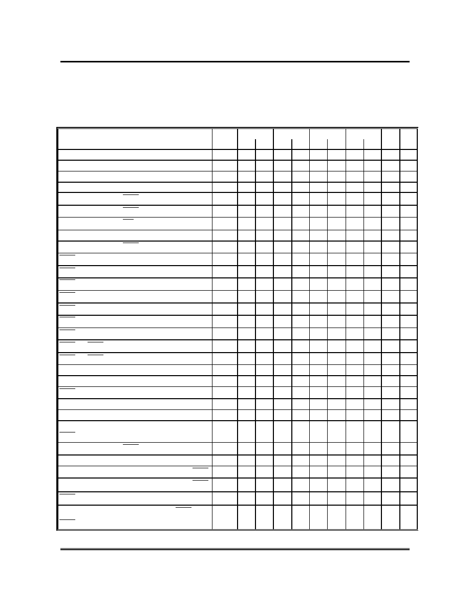
DC CHARACTERISTICS
(Ta = 0 to 70
∞
C, Vcc = 5V
±
10%, Vss = 0V)
-30
-35
-45
-60
Parameter
Symbol
Min Max Min Max Min Max Min Max
Unit
Test Condition
Operating Current
Icc1
- 200 - 180 - 160 - 140 mA RAS , CAS cycling
tRC=min
Standby Current
Icc2
-
4
-
4
-
4
-
4 mA
TTL interface,
RAS ,CAS =VIH,
DOUT=High-Z
Standby Current
Icc3
-
2
-
2
-
2
-
2 mA
CMOS interface,
RAS , CAS > Vcc-0.2V
Fast Page Mode Current
Icc4
- 200 - 180 - 160 - 140 mA RAS =VIL, CAS
cycling, tPC= min
RAS -only refresh
Current
Icc5
- 200 - 180 - 160 - 140 mA CAS =VIH, RAS
cycling, tRC= min
CAS Before RAS
Refresh Current
Icc6
- 200 - 180 - 160 - 140 mA
RAS ,CAS cycling,
tRC= min
Note: Icc depends on output load condition when the device is selected.
Icc max is specified at the output open condition, Icc is specified as an average current.
CAPACITANCE
(Ta =25
∞
C, Vcc =5V, f = 1M HZ)
Parameter
Symbol
Typ
Max
Unit
Input Capacitance
(address)
CI1
-
5
pF
Input Capacitance
(
RAS
,
CAS
,
WE
,
OE
)
CI2
-
7
pF
Output Capacitance
(data-in/out)
CI/O
-
10
pF
TE
CH
tm
T224160B
Taiwan Memory Technology, Inc. reserves the right
P. 5
Publication Date: MAR. 2001
to change products or specifications without notice.
Revision:B
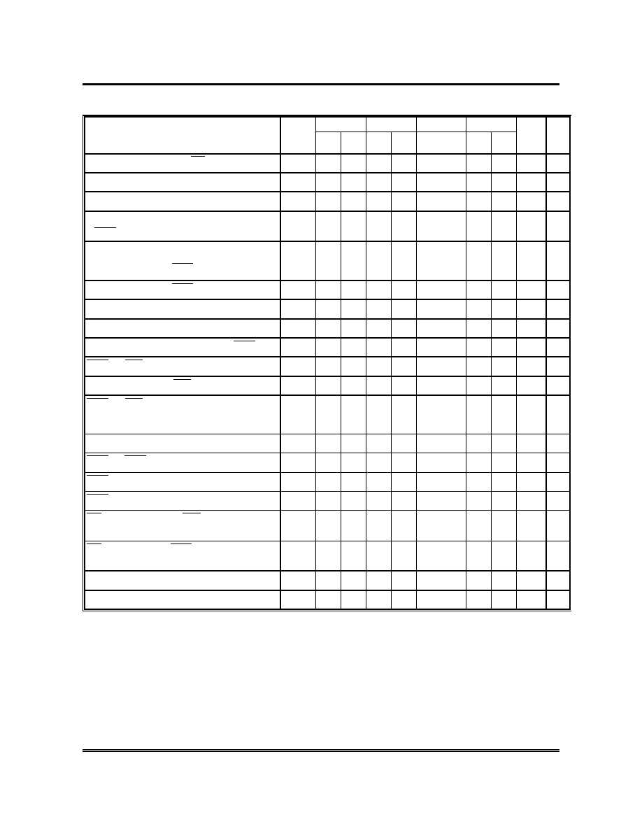
AC CHARACTERISTICS
(note 1,2,3) (Ta = 0 to 70
∞
C)
AC TEST CONDITIONS:
Vcc=5V
±
10%, input pulse level = 0 to 3V
Input rise and fall times: 2ns
Output Load: 2TTL gate + CL (50pF)
-30
-35
-45
-60
AC CHARACTERISTICS
PARAMETER
SYM
MIN MAX MIN MAX MIN MAX MIN MAX
UNIT
Note
s
Read or Write Cycle Time
tRC
55
65
85
110
ns
Read-Modify-Write Cycle Time
tRWC 85 95 115 155 ns
Fast-Page-Mode Read or Write Cycle Time
tPC
19
21
25
40
ns
Fast-Page-Mode Read-Write Cycle Time
tPCM 56 58 65 80 ns
Access Time From RAS
tRAC 30 35 45
60 ns
4
Access Time From CAS
tCAC
8
9
11
15 ns
5
Access Time From OE
tOAC
8
9
11
15 ns
13
Access Time From Column Address
tAA
13
15
19
30 ns
8
Access Time From
CAS
Precharge
tACP
15
18
22
35 ns
RAS Pulse Width
tRAS 30 10K 35 10K 45 10K 60 10K ns
RAS Pulse Width
tRASC 30
100K
35
100K
45
100K
60
100K
ns
RAS Hold Time
tRSH 8
9
11
15
ns
RAS Precharge Time
tRP
25
30
35
40
ns
CAS
Pulse Width
tCAS 5 10K 6 10K 7 10K 15 10K ns
CAS Hold Time
tCSH 30 35 45 60 ns
CAS
Precharge Time
tCP
3
3
5
10
ns
RAS to CAS Delay Time
tRCD 10 24 10 28 10 37 20 45 ns
7
CAS to RAS Precharge Time
tCRP 3
3
5
5
ns
Row Address Setup Time
tASR 0
0
0
0
ns
Row Address Hold Time
tRAH 5
5
5
5
ns
RAS to Column Address Delay Time
tRAD 8 17 8 20 8 26 15 30 ns
8
Column Address Setup Time
tASC 0
0
0
0
ns
Column Address Hold Time
tCAH 4
4
6
15
ns
Column Address Hold Time (Reference to
RAS )
tAR
26
30
40
50
ns
Column Address to RAS Lead Time
tRAL 13 15 19 30 ns
Read Command Setup Time
tRCS 0
0
0
0
ns
14
Read Command Hold Time Reference to
CAS
tRCH 0
0
0
0
ns
9,14
Read Command Hold Time Reference to RAS
tRRH 0
0
0
0
ns
9
CAS
to Output in Low-Z
tCLZ 3
3
3
3
ns
Output Buffer Turn-off Delay From CAS or
RAS
tOFF1 3 15 3 15 3 15 3 15
ns
10,16
TE
CH
tm
T224160B
Taiwan Memory Technology, Inc. reserves the right
P. 6
Publication Date: MAR. 2001
to change products or specifications without notice.
Revision:B
AC CHARACTERISTICS
(continued)
-30
-35
-45
-60
AC CHARACTERISTICS
PARAMETER
SYM
MIN MAX MIN MAX MIN MAX MIN MAX UNIT
Note
s
Output Buffer Turn-off OE to
tOFF2
-
8
-
8
-
8
-
15 ns
16
Write Command Setup Time
tWCS 0
0
0
0
ns
11,14
Write Command Hold Time
tWCH 4
4
6
10
ns
Write Command Hold Time (Reference
to
RAS
)
tWCR 26
30
46
50
ns
14
Write Command Pulse Width
tWP
4
4
6
10
ns
14
Write Command to RAS Lead Time
tRWL 6
7
9
15
ns
14
Write Command to CAS Lead Time
tCWL 6
7
9
15
ns
14
Data-in Setup Time
tDS
0
0
0
0
ns
12
Data-in Hold Time
tDH
4
4
6
15
ns
12
Data-in Hold Time (Reference to RAS )
tDHR 26 30
40
50
ns
RAS to WE Delay Time
tRWD 46 51
61
85
ns
11
Column Address to
WE
Delay Time
tAWD 29
31
35
55
ns
11
CAS to WE Delay Time
tCWD 24 25
27
40
ns
11
Transition Time (rise or fall)
tT
1.5 50 2.5 50 2.5 50
3
50 ns
2,3
Refresh Period (512 cycles)
tREF
8
8
8
8
ms
RAS to CAS Precharge Time
tRPC 10 10
10
10
ns
CAS
Setup Time (CBR REFRESH)
tCSR 10
10
10
10
ns
6
CAS Hold Time (CBR REFRESH)
tCHR 10 10
10
10
ns
6
OE Hold Time From WE During Read-
Modify-Write Cycle
tOEH 4
4
6
15
ns
15
OE Setup Prior to RAS During Hidden
Refresh Cycle
tORD 0
0
0
0
ns
Write Command Hold Time (Test Mode in) tWTH 10 10
10
10
ns
Write Command Setup Time (Test Mode in) tWTS 10
10
10
10
ns

TE
CH
tm
T224160B
Taiwan Memory Technology, Inc. reserves the right
P. 7
Publication Date: MAR. 2001
to change products or specifications without notice.
Revision:B
Notes:
1. An initial pause of 200us is required after
power-up followed by eight RAS refresh
cycles (
RAS
only or CBR) before proper
device operation is assured. The eight RAS
cycle wake -ups should be repeated any time
the tREF refresh requirement is exceeded.
2. VIH(2.4V) and VIL(0.8V) are reference
levels for measuring timing of input signals.
Transition times are measured between
VIH(2.4V) and VIL(0.8V).
3. In addition to meet the transition rate
specification, all input signals must transit
between VIH and VIL in a monotonic manner.
4. Assume that tRCD < tRCD(max). If tRCD is
greater than the maximum recommended value
shown in this table, tRAC will increase by the
amount that tRCD exceeds the value shown.
5. Assume that tRCD
tRCD(max) .
6. Enables on-chip refresh and address counters.
7. Operation within the tRCD(max) limit ensures
that tRAC(max) can be met. tRCD(max) is
specified as a reference point only; if tRCD is
greater than the specified tRCD(max) limit,
access time is controlled by tCAC.
8. Operation within the tRAD limit ensures that
tRAC(max) can be met. tRAD(max) is
specified as a reference point only; if tRAD is
greater than the specified tRAD(max) limit,
access time is controlled by tAA.
9. Either tRCH or tRRH must be satisfied for a
READ cycle.
10. tOFF1(max) defines the time at which the
output achieves the open circuit condition; it is
not a reference to VOH or VOL.
11. tWCS, tRWD, tAWD and tCWD are
restrictive operating parameters in LATE
WRITE and READ-MODIFY -WRITE cycles
only. If tWCS
tWCS(min), the cycle is an
EARLY WRITE cycle and the data output will
remain an open circuit throughout the entire
cycle. If tRWD
tRWD(min), tAWD
tAWD(min) and tCWD
tCWD(min), the
cycle is READ-WRITE and the data output
will contain data read from the selected cell. If
neither of the above conditions is met, the state
of I/O (at access time and until CAS and
RAS or OE go back to VIH) is indeterminate.
OE held high and WE taken low after CAS
goes low result in a LATE WRITE (OE -
controlled) cycle.
12. These parameters are referenced to CAS
leading edge in EARLY WRITE cycles and
WE leading edge in LATE WRITE or READ-
MODIFY-WRITE cycles.
13. During a READ cycle, if OE is low then taken
HIGH before CAS goes high, I/O goes open,
if OE is tied permanently low, a LATE
WRITE or READ-MODIFY-WRITE
operation is not possible.
14. WRITE command is defined as
WE
going low.
15. LATE WRITE and READ-MODIFY-WRITE
cycles must have both tOFF2 and tOEH met
( OE high during WRITE cycle) in order to
ensure that the output buffers will be open
during the WRITE cycles.
16. The I/Os open during READ cycles once
tOFF1 or tOFF2 occur.
TE
CH
tm
T224160B
Taiwan Memory Technology, Inc. reserves the right
P. 8
Publication Date: MAR. 2001
to change products or specifications without notice.
Revision:B
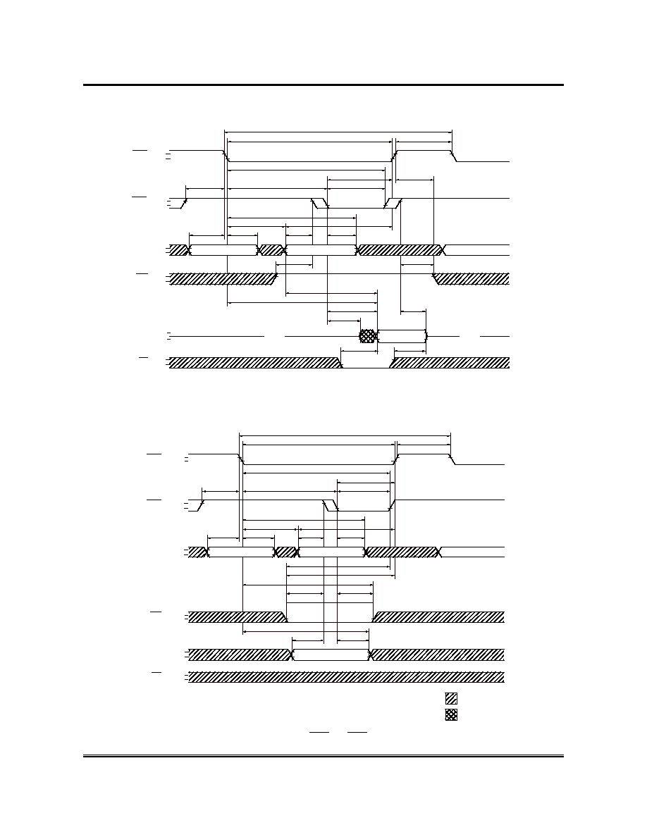
READ CYCLE
RA S
CA S
VIH
V IL
VOH
VOL
VIH
VIL
VIH
VIL
VIH
VIL
VIH
VIL
A DDR
WE
OE
I/O
t R A S
tR C
t R P
V A L ID D A T A
C O L U M N
R O W
R O W
tA S R
t R A H
tR A D
tC R P
t C S H
t R AL
tA S C
t C A H
tO F F 1
N O T E 1
t R R H
tA R
tA A
t C AC
t C L Z
t R AC
O P E N
O P E N
tO F F 2
tO A C
t R S H
t C A S
tR C D
tR C S
t RC H
EARLY WRITE CYCLE
RAS
C AS
V IH
V IL
V IOH
V IOL
V IH
V IL
V IH
V IL
V IH
V IL
V IH
V IL
A DDR
WE
OE
I/O
tR A S
tR C
tR P
V A L ID D A T A
C O L U M N
R O W
R O W
tA S R
tR A H
tR A D
tC R P
tC S H
tC W L
tR W L
tW C R
tA R
tD H R
tW P
t D S
tD H
tR S H
t C A S
t RC D
tW C H
tA S C
t C A H
t R A L
t WC S
DON'T CARE
UNDEFINED
Note: t
OFF1
is referenced from the rising edge of
RAS
or
CAS
, whichever occurs last.

TE
CH
tm
T224160B
Taiwan Memory Technology, Inc. reserves the right
P. 9
Publication Date: MAR. 2001
to change products or specifications without notice.
Revision:B
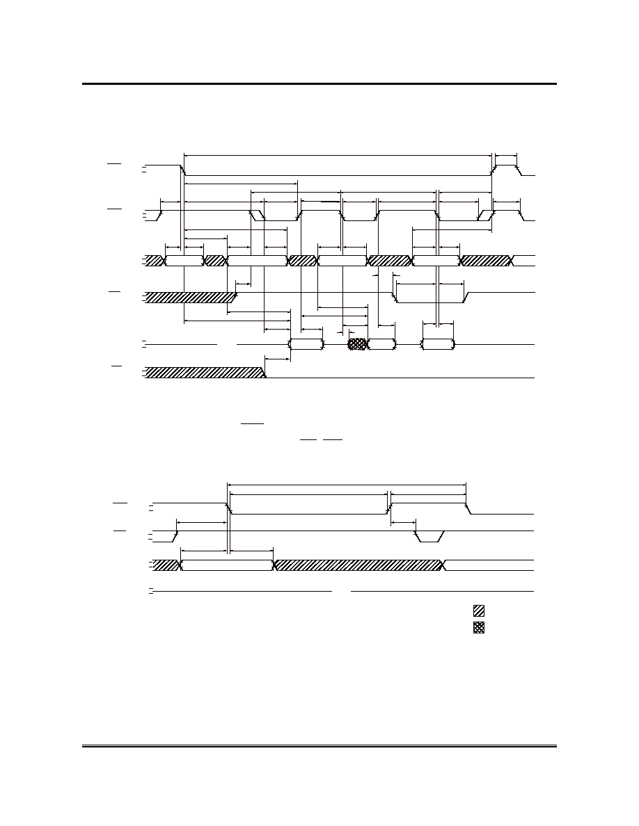
READ WRITE CYCLE
(LATE WRITE and READ-MODIFY-WRITE CYCLES)
RA S
CA S
VIH
V IL
VIOH
V IOL
VIH
V IL
VIH
V IL
VIH
V IL
VIH
V IL
ADDR
WE
OE
I/O
tR A S
tR WC
tR P
V A LID D
O U T
C O L U M N
R O W
R O W
tA S R
tR A H
tR AD
tC R P
tC S H
tR AL
tA S C
tC A H
tA R
tA A
tC AC
tC L Z
tR A C
O P E N
O P E N
tOF F 2
tOA C
tR S H
tC A S
tRC D
tR C S
tOE H
V A L ID D
IN
t DH
tD S
tR WD
tC WD
tA WD
tC WL
tR WL
tWP
FAST-PAGE-MODE READ CYCLE
Note: 1. t
OFF1
is referenced from the rising edge of RAS or CAS , whichever occurs last.
2. t
PC
can be measured from falling edge of CAS to falling edge of CAS , or from rising edge of
CAS to rising edge of CAS . Both measurements must meet the t
PC
specification.
RAS
CAS
VIH
VIL
VOH
VOL
VIH
VIL
VIH
VIL
VIH
VIL
VIH
VIL
ADDR
WE
OE
I / O
tRP
VALID
DATA
COLUMN
ROW
ROW
tASR tRAH
tRAD
tCRP
tRAL
tASC
tCAH
tAR
tAA
tCAC
tCLZ
tRAC
OPEN
OPEN
tOFF2
tOAC
tCSH
tRCD
tRCS
DON'T CARE
UNDEF INED
t RASC
tCPN
tRSH
tCP
tPC
tCP
tCAS
COLUMN
tASC
tCAH
tASC
tCAH
COLUMN
VALID
DATA
tCLZ
tCLZ
tAA
tCAC
tAA
tCAC
tOFF2
tOAC
tOFF1
tACP
tACP
tRRH
tRCH
tCAS
tCAS
VALID
DATA
tOFF2
tOAC
tOFF1
tOFF1

TE
CH
tm
T224160B
Taiwan Memory Technology, Inc. reserves the right
P. 10
Publication Date: MAR. 2001
to change products or specifications without notice.
Revision:B
FAST-PAGE-MODE EARLY-WRITE CYCLE
RAS
CA S
VIH
VIL
VIOH
VIOL
VIH
VIL
VIH
VIL
VIH
VIL
VIH
VIL
ADDR
WE
OE
I/O
V A L ID D A T A
t C A S
t R C D
t C R P
t C S H
t P C
t C P
t C P
t R S H
t C P N
t R A S C
V A L ID D A T A
VA LID DA TA
C O LU MN
C O L U MN
C O L U MN
RO W
RO W
t A S R t R A H
t R A D
t A R
t A S C
t C A H
t A S C t C A H
t A S C t C A H
t R A L
t W C S
t W C H
t C W L
t W P
t W C S
t C W L
t W C H
t W P
t W C S
t C W L
t W C H
t W P
t D S
t W C R
t D H R
t D H
t D S
t D H
t D S
t D H
t R W L
t C A S
t C A S
FAST-PAGE-MODE READ-WRITE CYCLE
(LATE WRITE and READ-MODIFY-WRITE CYCLES)
VIOH
VIOL
VIH
VIL
OE
I/O
t D H
t C A C
t C L Z
O P E N
O P E N
t O F F 2
t O A C
D ON 'T CAR E
UNDEF INED
t A A
t O E H
t O F F 2
t O A C
t A C P
RAS
CAS
VIH
VIL
VIH
VIL
VIH
VIL
VIH
VIL
ADDR
WE
t R P
C O L U M N
RO W
RO W
t A S R t R A H
t R A D
t C R P
t R A L
t A S C
t C A H
t A R
t A A
t D S
t R A C
t C S H
t C A S
t R C D
t R C S
t R A S C
t C P N
t R S H
t C P
t C P
t C A S
t C A S
C O L U M N
t A S C t C A H
t A S C t C A H
C O L U M N
t A A
t A C P
t R W L
t C W L
t W P
t C W L
t W P
t R W D
t A W D
t C W D
t C W D
t A W D
t C W D
t A W D
t C W L
t W P
t O F F 2
t O A C
t D H
t D S
t DH
t DS
t C A C
t C L Z
t C A C
t C L Z
t P C M
VAL ID
DIN
VALI D
DO UT
VALI D
DIN
V ALI D
DOUT
V ALI D
DIN
VALI D
DOUT
Note: t
PC
can be measured from falling edge to falling edge of
CAS
, or from rising edge to rising edge of
CAS . Both measurements must meet the t
PC
specification.
TE
CH
tm
T224160B
Taiwan Memory Technology, Inc. reserves the right
P. 11
Publication Date: MAR. 2001
to change products or specifications without notice.
Revision:B
FAST-PAGE-MODE READ-EARLY-WRITE CYCLE
(Pseudo READ-MODIFY-WRITE)
RAS
ONLY REFRESH CYCLE
(ADDR=A0-A8 ;
OE
,
WE
=DON`T CARE)
RAS
CA S
VIH
VIL
V OH
V OL
VIH
VIL
VIH
VIL
ADDR
I/O
tR A S
t RC
tR P
O P E N
R O W
R O W
t A S R
tR A H
t C R P
tR P C
DON'T CARE
UNDEFINED
Note1:Do not drive data prior to tristate.
R A S
C A S
VIH
VIL
VIOH
VIOL
VIH
VIL
VIH
VIL
VIH
VIL
VIH
VIL
A D D R
WE
OE
I / O
tRP
VALID
DATA (B)
ROW
ROW
tASR tRAH
tRAD
tCRP
tCSH
tRAL
tASC
tCAH
tRASC
tRSH
tAR
t AA
tCAC
tRAC
OPEN
tOAC
tPC
tCAS
tRCD
tRCS
COLUMN(A)
COLUMN(B)
COLUMN(N)
NOTE1
VALID
DATA (A)
tCP
tPC
tCP
tCAS
tCAS
tCP
tASC
tCAH
tASC
tCAH
tWCH
tWCS
tRCH
tOFF1
t AA
tCAC
tCLZ
tACP
tDS
tDH
tOFF1
VALID
DATA IN

TE
CH
tm
T224160B
Taiwan Memory Technology, Inc. reserves the right
P. 12
Publication Date: MAR. 2001
to change products or specifications without notice.
Revision:B
CBR REFRESH CYCLE
(A0-A8 ;
OE
=DON`T CARE)
RA S
C A S H, CA S L
VIH
VIL
VIH
VIL
VIH
VIL
I/O
tR A S
tR A S
t R P
O P E N
tR P C
tC P N
WE
tR P
tC S R
t C H R
t RP C
tC S R
tC H R
HIDDEN REFRESH CYCLE
(
WE
=HIGH ;
OE
=LOW)
R A S
C A S
V IH
V IL
V OH
V O L
V IH
V IL
V IH
V IL
I /O
( R E F R E S H )
t R A S
t R P
O P E N
V A L I D D A T A
t C R P
O E
O P E N
V IH
V IL
A D D R
R O W
t A S R
t R A H
t R A D
t R A L
t A S C
t C A H
t A R
t A A
t C A C
t C L Z
t R A C
t O A C
t R S H
t R C D
t C H R
C O L U M N
t O F F 2
tORD
t O FF 1
N O T E 1
( R E A D )
t R A S
Note: 1. t
OFF1
is referenced from the rising edge of
RAS
or
CAS
, whichever occurs last.

TE
CH
tm
T224160B
Taiwan Memory Technology, Inc. reserves the right
P. 13
Publication Date: MAR. 2001
to change products or specifications without notice.
Revision:B
PACKAGE DIMENSIONS
40-LEAD SOJ DRAM (400 mil)
SYMBOL
DIMENSIONS IN INCHES
DIMENSIONS IN MM
A
1.025±0.010
26.035±0.254
B
0.400±0.005
10.160±0.127
C
0.045(MAX)
1.143(MAX)
D
0.050±0.006
1.27±0.152
E
0.019±0.003
0.483±0.08
F
0.026±0.003
0.661±0.080
G
0.440±0.010
11.176±0.254
H
0.011±0.003
0.280±0.080
I
0.025(MIN)
0.635(MIN)
J
0.364±0.020
9.246±0.508
K
0.047±0.006
1.194±0.152
L
0.150(MAX)
3.810(MAX)
y
0.004(MAX)
0.102(MAX)

TE
CH
tm
T224160B
Taiwan Memory Technology, Inc. reserves the right
P. 14
Publication Date: MAR. 2001
to change products or specifications without notice.
Revision:B
PACKAGE DIMENSIONS
40-LEAD TSOP II DRAM (400 mil)
SYMBOL
DIMENSIONS IN INCHES
DIMENSIONS IN MM
A
0.047(max)
1.20(max)
A1
0.004±0.002
0.10±0.05
A2
0.039±0.002
1.00±0.05
b
0.014(typ.)
0.35(typ.)
c
0.005(typ.)
0.127(typ.)
D
0.725±0.004
18.41±0.10
E
0.463±0.008
11.76±0.20
E1
0.400±0.004
10.16±0.10
L1'
0.031
0.80
L'
0.020±0.004
0.500±0.10
y
0.004(max)
0.10(max)
0
∞
~5
∞
0
∞
~5
∞
"A"