
TE
CH
tm
T35L6432B
Taiwan Memory Technology, Inc. reserves the right P. 1
Publication Date: JUL. 2002
to change products or specifications without notice.
Revision: A
SYNCHRONOUS
BURST SRAM
64K x 32 SRAM
Flow-Through Burst Mode
FEATURES
�
Fast Access times: 9 / 10 / 11 / 12 ns
�
Single 3.3V (+0.3V/-0.165V) power supply
�
Common data inputs and data outputs
�
Individual BYTE WRITE ENABLE and
GLOBAL WRITE control
�
Three chip enables for depth expansion and
address pipelining
�
Clock-controlled and registered address, data
I/Os and control signals
�
Internally self-timed WRITE CYCLE
�
Burst control pins ( interleaved or linear burst
sequence)
�
High 30pF output drive capability at rated access
time
�
SNOOZE MODE for reduced power standby
�
Burst Sequence :
- Interleaved (MODE=NC or VCC)
- Linear (MODE=GND)
OPTIONS
MARKING -9
-10
-11 -12
Access
time
9ns 10ns 11ns 12ns
Flow-
through
2-1-1-1 Cycle
time
10.5ns 15ns 15ns 15ns
PACKAGE package code
100-pin QFP Q
100-pin TQFP T
Part Number Examples
PART NO.
speed
Package
T35L6432B-10Q 10ns
QFP
T35L6432B-12T 12ns
TQFP
GENERAL DESCRIPTION
The Taiwan Memory Technology Synchronous
Burst RAM family employs high-speed, low power
CMOS design using advanced triple-layer polysilicon,
double-layer metal technology. Each memory cell
consists of four transistors and two high valued resistors.
The T35L6432B SRAM integrates 65536 x 32
SRAM cells with advanced synchronous peripheral
circuitry and a 2-bit counter for internal burst operation.
All synchronous inputs are gated by registers controlled
by a positive-edge-triggered clock input (CLK). The
synchronous inputs include all addresses, all data inputs,
address-pipelining chip enable (
CE
), depth-
expansion chip enables (
CE2
and CE2), burst control
inputs (
ADSC
,
ADSP
, and
ADV
), write enables
(
BW1
,
BW2
,
BW3
,
BW4
, and
BWE
), and
global write (
GW
).
Asynchronous inputs include the output enable
(
OE
), Snooze enable (ZZ) and burst mode control
(MODE). The data outputs (Q), enabled by
OE
, are
also asynchronous.
Addresses and chip enables are registered with
either address status processor (
ADSP
) or address
status controller (
ADSC
) input pins. Subsequent burst
addresses can be internally generated as controlled by
the burst advance pin (
ADV
).
Address and write controls are registered on-chip
to initiate self-timed WRITE cycle. WRITE cycles
can be one to four bytes wide as controlled by the write
control inputs. Individual byte write allows individual
byte to be written.
BW1
controls DQ1-DQ8.
BW2
controls DQ9-DQ16.
BW3
controls DQ17-
DQ 24.
BW4
controls DQ25-DQ32.
BW1
,
BW2
,
BW3
, and
BW4
can be active only with
BWE
being LOW.
GW
being LOW causes all
bytes to be written. WRITE pass-through capability
allows written data available at the output for the
immediately next READ cycle. This device also
incorporates pipelined enable circuit for easy depth
expansion without penalizing system performance.

TE
CH
tm
T35L6432B
Taiwan Memory Technology, Inc. reserves the right P. 2
Publication Date: JUL. 2002
to change products or specifications without notice.
Revision: A
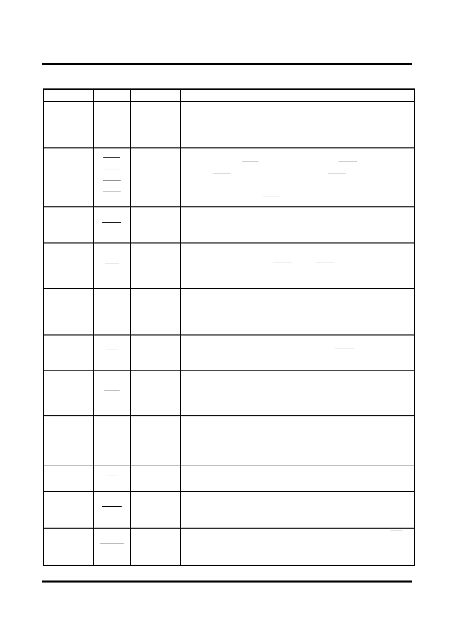
FUNCTIONAL BLOCK DIAGRAM
Note: The Functional Block Diagram illustrates simplified device operation. See Truth Table,
pin descriptions and timing diagrams for detailed information.
BYTE 4
WRITE REGISTER
ENABLE
REGISTER
BYTE 1
WRITE REGISTER
BYTE 3
WRITE REGISTER
BYTE 2
WRITE REGISTER
ADDRESS
REGISTER
BINARY
COUNTER
& LOGIC
CLR
Q0
16
16
14
16
A0
A1
A1'
A0'
64K x 8 x 4
MEMORY
ARRAY
SENSE
AMPS
INPUT
REGISTERS
8
8
8
8
8
8
8
8
32
32
32
DQ1
.
.
.
DQ32
4
A0-A15
MODE
ADV
CLK
ADSC
ADSP
BW4
BW3
BW2
BW1
CE
CE2
CE2
OE
GW
BWE
Q1
OUTPUT
BUFFERS
BYTE 1
WRITE DRIVER
BYTE 2
WRITE DRIVER
BYTE 3
WRITE DRIVER
BYTE 4
WRITE DRIVER

TE
CH
tm
T35L6432B
Taiwan Memory Technology, Inc. reserves the right P. 3
Publication Date: JUL. 2002
to change products or specifications without notice.
Revision: A
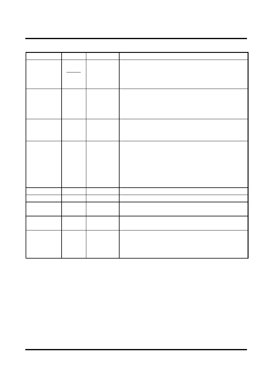
PIN ASSIGNMENT (Top View)
N C
D Q 1 7
D Q 1 8
V C C Q
V S S Q
D Q 1 9
D Q 2 0
D Q 2 1
D Q 2 2
V S S Q
V C C Q
D Q 2 3
D Q 2 4
N C
V C C
N C
V S S
D Q 2 5
D Q 2 6
V C C Q
V S S Q
D Q 2 7
D Q 2 8
D Q 2 9
D Q 3 0
V S S Q
V C C Q
D Q 3 1
D Q 3 2
N C
N C
D Q 1
D Q 2
V C C Q
V S S Q
D Q 3
D Q 4
D Q 5
D Q 6
V S S Q
V C C Q
D Q 7
D Q 8
Z Z
V C C
N C
V S S
D Q 9
D Q 1 0
V C C Q
V S S Q
D Q 1 1
D Q 1 2
D Q 1 3
D Q 1 4
V S S Q
V C C Q
D Q 1 5
D Q 1 6
N C
1
1 1
1 0
9
8
7
6
5
4
3
2
1 8
1 7
1 6
1 5
1 4
1 3
1 2
2 8
2 7
2 6
2 5
2 4
2 3
2 2
2 1
2 0
1 9
3 0
2 9
3 1
4 1
4 0
3 9
3 8
3 7
3 6
3 5
3 4
3 3
3 2
4 9
4 8
4 7
4 6
4 5
4 4
4 3
4 2
5 0
6 0
5 9
5 8
5 7
5 6
5 5
5 4
5 3
5 2
5 1
7 0
6 9
6 8
6 7
6 6
6 5
6 4
6 3
6 2
6 1
8 0
7 9
7 8
7 7
7 6
7 5
7 4
7 3
7 2
7 1
9 5
9 6
8 8 8 7 8 6 8 5 8 4 8 3 8 2 8 1
9 0
9 1
9 2
9 3
9 4
8 9
1 0 0 9 9 9 8 9 7
A7
A6
BW
E
GW
CL
K
VS
S
VC
C
CE
2
BW
1
BW
2
BW
3
BW
4
CE
2
CE
AD
V
AD
S
P
AD
S
C
OE
A9
A8
NC
VC
C
NC
NC
A1
0
A0
NC
VS
S
A1
1
A1
2
A1
3
A1
4
A1
5
NC
A1
A2
A3
MO
D
E
A4
A5
1 0 0 -p in Q F P
o r
1 0 0 -p in T Q F P
TE
CH
tm
T35L6432B
Taiwan Memory Technology, Inc. reserves the right P. 4
Publication Date: JUL. 2002
to change products or specifications without notice.
Revision: A
PIN DESCRIPTIONS
PINS SYM. TYPE
DESCRIPTION
32-37, 44-49,
81, 82, 99,
100,
A0-A15
Input-
Synchronous
Addresses: These inputs are registered and must meet the setup and
hold times around the rising edge of CLK. The burst counter
generates internal addresses associated with A0 and A1, during
burst cycle and wait cycle.
93-96
BW1
BW2
BW3
BW4
Input-
Synchronous
Byte Writes: A byte write is LOW for a WRITE cyle and HIGH for
a READ cycle. BW1 controls DQ1-DQ8. BW2 controls DQ9-
DQ16. BW3 controls DQ17-DQ24. BW4 controls DQ25-
DQ32. Data I/O are high impedance if either of these inputs are
LOW , conditioned by
BWE
being LOW.
87
BWE
Input-
Synchronous
Write Enable: This active LOW input gates byte write operations
and must meet the setup and hold times around the rising edge of
CLK.
88
GW
Input-
Synchronous
Global Write: This active LOW input allows a full 32-bit WRITE to
occur independent of the BWE and BWn lines and must meet
the setup and hold times around the rising edge of CLK.
89 CLK
Input-
Synchronous
Clock: This signal registers the addresses, data, chip enables,
writecontrol and burst control inputs on its rising edge. All
synchronous inputs must meet setup and hold times around the
clock's rising edge.
98
CE
Input-
Synchronous
Synchronous Chip Enable: This active LOW input is used to enable
the device and conditions internal use of
ADSP
. This input is
sampled only when a new external address is loaded.
92
CE2
Input-
Synchronous
Synchronous Chip Enable: This active LOW input is used to enable
the device. This input is sampled only when a new external address
is loaded. This input can be used for memory depth expansion.
97 CE2
Input-
Synchronous
Synchronous Chip Enable: This active HIGH input is used to enable
the device. This input is sampled only when a new external address
is loaded. This input can be used for memory depth expansion.
86
OE
Input
Output enable: This active LOW asynchronous input enables the
data output drivers.
83
ADV
Input-
Synchronous
Address Advance: This active LOW input is used to control the
internal burst counter. A HIGH on this pin generates wait cycle
(no address advance).
84
ADSP
Input-
Synchronous
Address Status Processor: This active LOW input, along with
CE
being LOW, causes a new external address to be registered and a
READ cycle is initiated using the new address.
TE
CH
tm
T35L6432B
Taiwan Memory Technology, Inc. reserves the right P. 5
Publication Date: JUL. 2002
to change products or specifications without notice.
Revision: A
PIN DESCRIPTIONS
(continued)
QFP PINS
SYM.
TYPE
DESCRIPTION
85
ADSC
Input-
Synchronous
Address Status Controller:This active LOW input causes
device to be deselected or selected along with new external
address to be registered. A READ or WRITE cycle is
initiated depending upon write control inputs.
31 MODE
Input-
Static
Mode: This input selects the burst sequence. A LOW on this
pin selects LINEAR BURST. A NC or HIGH on this pin
selects INTERLEAVED BURST. Do not alter input state
while device is operating.
64 ZZ
Input
Snooze Enable: This active HIGH asynchronous input causes
the device to enter a low-power standby mode in which all
data in the memory arry is retained.
2, 3, 6-9, 12, 13,
18, 19, 22-25,
28, 29, 52, 53,
56-59, 62, 63,
68, 69, 72-75,
78, 79,
DQ1-
DQ32
Input/
Output
Data Inputs/Outputs: First Byte is DQ1-DQ8. Second Byte is
DQ9-DQ16. Third Byte is DQ17-DQ24. Fourth Byte is DQ25-
DQ32. Input data must meet setup and hold times around the
rising edge of CLK.
15,41,65,91
VCC
Supply
Power Supply: 3.3V (+0.3V/-0.165V)
17,40,67,90 VSS Ground
Ground:
GND
4,11,20,27,54,
61,70,77
VCCQ
I/O Supply Output Buffer Supply: 3.3V (+0.3V/-0.165V)
5,10,21,26,55,
60,71,76
VSSQ
I/O Ground Output Buffer Ground: GND
1,14,16,30,38,
39,42,43,50,51,
66,80
NC
-
No Connect: These signals are not internally conntected.