
TE
CH
tm
T62M0002A
TM Technology Inc. reserves the right P. 1 Publication Date: JUL. 2002
to change products or specifications without notice. Revision:A
T62M0002A
Digital
Sound
Processor
Embedded
SRAM
Features
! Operating voltage: 4.5V ~ 5.5V
! ADM algorithm
! Low noise ( -88dB typical)
! Low distortion rate (0.5% typical)
! Embedded SRAM
! Automatic reset function
! Package type: 16-pin DIP/SOP
Description
The T62M0002A is an echo/surround effect processor.
It is designed for various audio systems including
karaoke, television, sound equipment, etc. The chip
consists of a built-in pre-amplifier, VCO or Voltage
control OSC, Embedded SRAM, A/D and D/A
converters as well as delay time control logic. Its
built-In reply to SRAM can generate delay time effect
and can control the delay time value through the
external VCO resistor. The VCO circuit can reduce
external components and make it easy to adjust the
delay time.
Part Number Examples
Part NO.
Pkg
Description
T62M0002A-j 16-SOP
300mil-16-SOP
T62M0002A-K 16-DIP 300mil-16-DIP
TE
CH
tm
T62M0002A
TM Technology Inc. reserves the right P. 2 Publication Date: JUL. 2002
to change products or specifications without notice. Revision:A
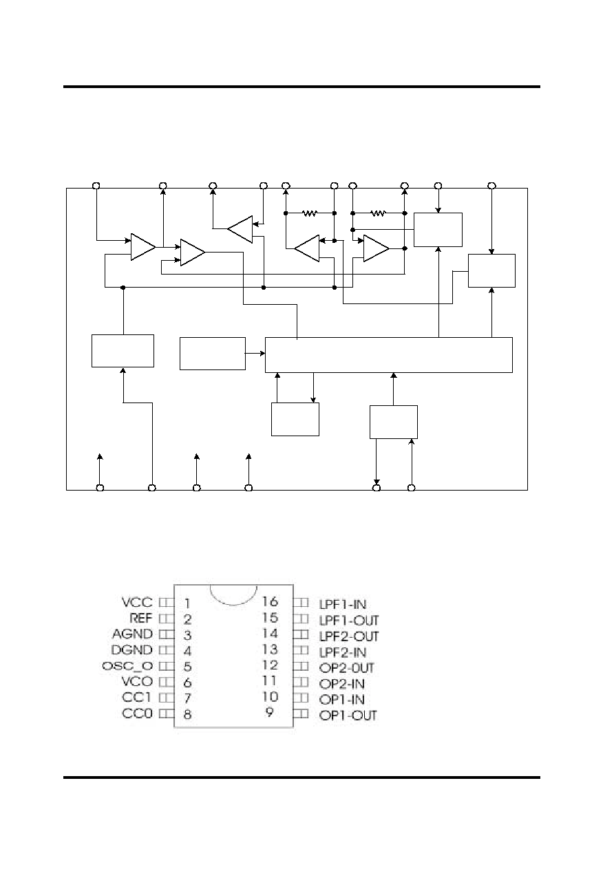
Block Diagram
+
-
+
-
-
+
+
-
-
+
M O D
D E M
D I D O 0 D O 1
MO MI C LO C K
1 /2
VC C
AU T O
R E S E T
VC O
R AM
LP F1
IN
LP F1
O UT
LP F2
O UT
LP F2
IN
O P 2
O UT
O P 2
IN
O P 1
IN
O P 1
O UT
C C 0
C C 1
V C C
R EF
A GN D
D GN D
O S C _ O
V C O
4 .7 K
O h m
4 .7 K
O h m
LP F1
C O M P
LP F2
PIN Configuration
T62M0002A

TE
CH
tm
T62M0002A
TM Technology Inc. reserves the right P. 3 Publication Date: JUL. 2002
to change products or specifications without notice. Revision:A
PIN Description
Pin NO. Pin Name I/O
Description
1
VCC
-
Analog and positive power supply
2
REF
I
Analog reference voltage
3 AGEND -
Analog
ground
4 DGEND -
Digital
ground
5
OSC_O
I
System oscillator output
6
VCO
I
System oscillator input,system frequency adjustable pin
7 CC1 -
Current
control1
8 CC2 -
Current
control2
9 OP1_OUT O
OP1
output
10 OP1_IN I
OP1
input
11 OP2_IN I
OP2
input
12 OP2_OUT O
OP2
output
13
LPF2_IN
I
Low pass filter2 input
14
LPF2_OUT
O Low pass filter2 output
15
LPF1_OUT
O Low pass filter1 output
16
LPF1_IN
I
Low pass filter1 input
Function Description
The T62M0002A is an echo/surround effect generator with built-in SRAM. It enaures low
distortion as well as low noise for processing audio signal delay. The chip provides two playing
modes(echo and surround) and the playing function block diagrams are shown as follows.
- Surround
Mode
Vin LPF1
A/D Delay D/A LPF2 Vout
-Echo Mode
Vout
Vin LPF1
A/D Delay D/A LPF2

TE
CH
tm
T62M0002A
TM Technology Inc. reserves the right P. 4 Publication Date: JUL. 2002
to change products or specifications without notice. Revision:A
Electrical Characteristics
Ta=25�C
Test Conditions
Symbol Parameter
VDD Conditions
Min. Typ. Max. Unit
V
CC
Operating
Voltage
-
-
4.5
5.0
5.5
V
I
CC
Operating
Current
5V
-
-
15
30 mA
G
V
Voltage
Gain
5V
R
L
=47K
- 0.5 2.5 dB
V
OMAX
Maximum Output Voltage
5V
THD=10%
1.0
1.6
-
Vrms
THD
Total Harmonic Distortion
5V
30KHz L.P.F.
-
0.5
1.5
%
No
Output Noise Voltage
5V
DIN Audio
-
-88
-80
dbV
Absolute Maximum Ratings
Supply Voltage .......................................................... -0.3V to 6V
Input Voltage ............................................................ Vss-0.3V to VDD+0.3V
Storage Temperature .................................................... -50
�C to 125�C
Operating Temperature .................................... -20�C to 70�C
Note: These are stress ratings only. Stresses exceeding the range specified under "Absolute
Maximum Ratings" may cause substantial damage to the device. Functional operation of this
device at other conditions beyond those listed in the specification is not implied and prolonged
exposure to extreme conditions may affect device reliability.

TE
CH
tm
T62M0002A
TM Technology Inc. reserves the right P. 5 Publication Date: JUL. 2002
to change products or specifications without notice. Revision:A
Application Circuits
C26
0.1uF
C23
1uF
C15
4700pF
R16
20K
C29
0.33uF
R21
18K
C28
0.1uF
R20
Radj
R14
18k
C25
560pF
C22
4.7uF
C16
4.7uF
R22
20K
C17
1uF
C21
100uF
AGND
R19
10K
R13
2.7k
INPUT
C18
560pF
DGND
R15
5.6K
R12
10k
C24
0.01uF
OUPUT
Echo Mode
C20
0.1uF
R10
20k
R11
100K
C19
1uF
R17
50K
3
2
1
VCC
C27
4700pF
R18
3K
U2
T62M0002A
1
2
3
4
5
6
7
8
9
10
11
12
13
14
15
16
VCC
REF
AGND
DGND
OSC_O
VCO
CC1
CC0
OP1-OUT
OP1-IN
OP2-IN
OP2-OUT
LPF2-IN
LPF2-OUT
LPF1-OUT
LPF1-IN
C30
0.33uF
C9
0.01uF
C11
4700pF
C6
4.7uF
R1
10k
R6
18K
INPUT
C12
0.1uF
R9
20K
R2
20k
R7
10K
C14
0.33uF
C8
560pF
AGND
C10
0.1uF
C2
4.7uF
R4
18k
C7
1uF
VCC
R3
100K
Surround Mode
C13
0.33uF
R5
2.7k
DGND
U1
T62M0002A
1
2
3
4
5
6
7
8
9
10
11
12
13
14
15
16
VCC
REF
AGND
DGND
OSC_O
VCO
CC1
CC0
OP1-OUT
OP1-IN
OP2-IN
OP2-OUT
LPF2-IN
LPF2-OUT
LPF1-OUT
LPF1-IN
R8
Radj
C4
0.1uF
C1
4700pF
C5
100uF
OUPUT
C3
560pF
Note:"Radj" Value con set delay time. R/delay time Reference on Resistance / Delay Time
Table.

TE
CH
tm
T62M0002A
TM Technology Inc. reserves the right P. 6 Publication Date: JUL. 2002
to change products or specifications without notice. Revision:A
Resistance / Delay Time Table .
FCK 2.0M 2.5M 3.0M 3.5M 4.0M 4.5M 5.0M 5.5M
Radj 53.40k 41.97k 33.41k 28.18k 24.00k 20.90k 18.20k 16.00k
TD 264ms 226ms 174ms 150ms 130ms 117ms 106ms 95.2ms
THD+N
%
1.29% 0.95% 0.73% 0.57% 0.48% 0.41% 0.37% 0.33%
FCK 6.0M 6.5M 7.0M 7.5M 8.0M 8.5M 9.0M 10M
Radj 14.50k 12.90k 11.60k 10.70k 9.72k 9.07k 8.07k 6.98k
TD 89ms 80.8ms 74.8ms 70.4ms 65.2ms 62.4ms 57.6ms 52.4ms
THD+N
%
0.29% 0.28% 0.25% 0.24% 0.22% 0.22% 0.21% 0.18%
FCK 11M 12M 13M 14M 15M 16M 17M 18M
Radj 5.99k 5.30k 4.52k 4.02k 3.48k 3.08k 2.64k 2.30k
TD 47.6ms 44.2ms 40.2ms 37.6ms 35.0ms 33.0ms 30.8ms 29.0ms
THD+N
%
0.17% 0.15% 0.14% 0.14% 0.14% 0.14% 0.14% 0.14%
FCK 19M 20M 21M 22M
Radj 2.16k 1.89k 1.69k 1.49k
TD 27.8ms
26.2ms 25.0ms 24.0ms
THD+N
%
0.14% 0.14% 0.14% 0.14%
Note :This Table is for Surround Mode.
R= Extend Resister for adjust FCK & TD.
FCK= Oscillate output Frequency for Pin 5 .(Unit : MHZ)
TD=Delay Time for output.
THD=Total Harmonic Distortion. (TDH+N Ratio %)
1 H Z
5 n s
5 m s
2 .0 VP P
2 VD C
Pulse Clock Waveform for input Pin
TE
CH
tm
T62M0002A
TM Technology Inc. reserves the right P. 7 Publication Date: JUL. 2002
to change products or specifications without notice. Revision:A
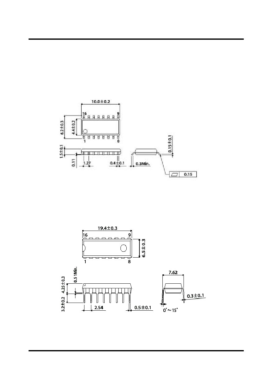
IC Package
T62M0002A 16-SOP
Unit:mm
T62M0002A 16-DIP
Unit:mm