 | –≠–ª–µ–∫—Ç—Ä–æ–Ω–Ω—ã–π –∫–æ–º–ø–æ–Ω–µ–Ω—Ç: T6311A-D | –°–∫–∞—á–∞—Ç—å:  PDF PDF  ZIP ZIP |
TE
CH
tm
Preliminary Product spec. T6311A
TM Technology Inc. reserves the right P. 1
Publication Date: JUN. 2005
to change products or specifications without notice.
Revision: C
Low-Dropout, Constant-Current
White LED Bias Supply
FEATURES
∑ Low 200mV Dropout at 9mA
∑ Up to 150mA LED Bias Current
∑ 0.3% LED Current Matching
∑ Simple LED Brightness Control
∑ Low 40uA Supply Current
∑ Low 0.05uA Shutdown Current
∑ 2.5V to 5.5V Supply Voltage Range
∑ SOP-8 and SOT23-6 Package
∑ Output channel :
SOP-8 package for four channel
SOT23-6 package for three channel
Applications
∑ Cellular Phones
∑ Portable Communication Devices
∑ Handheld Electronics
∑ Digital Cameras
∑ PDAs
∑ LED/Display Back Light Driver
∑ LEDs for Camera Flash
PART NUMBER EXAMPLES
GRNERAL DESCRIPTION
The T6311A low-dropout bias supply for
white LEDs is a high-performance alternative
to the simple ballast resistors used in
conventional white LED designs. The T6311A
uses a single resistor to set the bias current for
four LEDs, which are matched to 0.3%. The
T6311A consumes only 40uA of supply
current when enabled and 0.05uA when
disabled. The T6311A advantages over ballast
resistors include significantly better LED to
LED bias matching, much lower bias variation
with supply voltage variation, significantly
lower dropout voltage, and in some
applications, significantly improved efficiency.
The T6311A requires a 200mV dropout at a
9mA load on each output to match the LED
brightness. The T6311A is available in SOP-8
and SOT23-6 package.
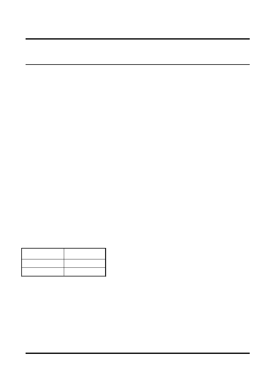
PART NO.
PACKAGE
T6311A-D SOP-8
T6311A-X SOT23-6

TE
CH
tm
Preliminary Product spec. T6311A
TM Technology Inc. reserves the right
P.2
Publication Date: JUN. 2005
to change products or specifications without notice.
Revision: C
PIN ARRANGEMENT(Top view)
SOT23-6 SOP-8
GND
EN
SET
1
2
3
4
6
5
LED1
LED2
LED3
G N D
E N
S E T
1
2
3
6
8
7
L E D 1
L E D 2
L E D 3
N C
4
5
L E D 4
PIN DESCRIPTION
Pin no.
SYMBO
L
SOP-8 SOT23-6
DESCRIPTION
EN 8 1
Enable Input/Power Input. Drive high (> 2.5V) to enable; drive low (< 2.2V) to
disable. When disabled, SET, LED1, LED2, LED3 and LED4 are high impedance.
When enabled, EN is the power input for the T6311A.
GND 7 2
Ground
SET 6 3
Bias Current Set Input. The current flowing into SET sets the bias current into each
LED by ILED_= 240 x ISET. VSET is internally biased to 1.2V. SET is high
impedance when EN is low.
NC 5 -
No connection.
LED4 4 -
LED 4 Cathode Connection. Current flowing into LED4 is 240 times the current
flowing into SET. LED4 is high impedance when EN is low.
LED3 3 4
LED 3 Cathode Connection. Current flowing into LED3 is 240 times the current
flowing into SET. LED3 is high impedance when EN is low.
LED2 2 5
LED 2 Cathode Connection. Current flowing into LED2 is 240 times the current
flowing into SET. LED2 is high impedance when EN is low.
LED1 1 6
LED 1 Cathode Connection. Current flowing into LED1 is 240 times the current
flowing into SET. LED1 is high impedance when EN is low.

TE
CH
tm
Preliminary Product spec. T6311A
TM Technology Inc. reserves the right
P.3
Publication Date: JUN. 2005
to change products or specifications without notice.
Revision: C
BLOCK DIAGRAM
EN
REF
LED3
GND
-
+
LED2
LED1
SET
ON
OFF
V+
R
SET
V
CTRL
LED4
current
controller
Fig. 1

TE
CH
tm
Preliminary Product spec. T6311A
TM Technology Inc. reserves the right
P.4
Publication Date: JUN. 2005
to change products or specifications without notice.
Revision: C
ABSOLUTE MAXIMUM RATINGS
Parameter
Symbol
Value
Unit
Voltage on any pin relative to GND
V
IN
-0.3 to 6
V
Operating Temperature Rang
T
A
-40 to +85
∞
C
Maximum Soldering Temperature (at leads, 10 sec)
T
LEAD
300
∞
C
Storage Temperature Rang
T
S
-65 to +150
∞
C
Continuous Power Dissipation ( T
A
= +70
∞
C )
1 W
Electrical Characteristics
(TA = -40 to 85∞C unless otherwise noted. Typical values are at TA =25∞C,
VEN =3.3V, VLED1 = VLED2= VLED3= VLED4= 1V) (Note 1)
Symbol Description
Conditions Min.
Typ.
Max
Unit
V
EN
Operating voltage range
EN is power supply input
2.5
5.5
V
I
SET
SET input current range
5
260
uA
SET to LED current ratio
I
LED
/ I
SET,
I
SET
=42uA
220 240 260 A/A
V
SET
SET bias voltage
I
SET
=42uA
1.08 1.2 1.32 V
T
A
= -40 to +25
∞
C
0.01 1 uA
SET leakage current in
Shutdown
EN=GND,
V
SET
=3.3V T
A
= -40 to +85
∞
C
5
uA
LED to LED current matching I
SET
=42uA
0.3 %
I
LED
Maximum LED sink current
Each LED
100 150
mA
I
SET
=20uA
(Note 2)
100
180 mV
I
SET
=40uA
(Note 3)
200
360 mV
LED dropout voltage
I
SET
=80uA
(Note 3)
230
410 mV
LED leakage current in
shutdown
V
LED1
=V
LED2
=V
LED3
=V
LED4
= 3.3V,
EN=GND, T
A
=+25
∞
C, each LED
0.01 1 uA
V
IH
Input high voltage
V
EN
>V
IH
for enable
2.5 V
V
IL
Input low voltage
V
EN
<V
IL
for disable
2.2
V
V
EN
= 2.50V to 5.5V, EN is power
supply input
40
100
uA
I
EN
EN intput bias current
V
EN
= 0.4V, T
A
=+25
∞
C
0.05 1 uA
Note 1: Limits are 100% production tested at TA = +25∞C. Limits over the operating temperature range are
guaranteed through correlation using statistical quality control (SQC) methods.
Note 2: Dropout Voltage is defined as the LED to GND voltage at which current sink into LED drops 20% from the
value at VLED = 1V.
Note 3: Dropout Voltage is defined as the LED to GND voltage at which current sink into LED drops 10% from the
value at VLED = 1V.

TE
CH
tm
Preliminary Product spec. T6311A
TM Technology Inc. reserves the right
P.5
Publication Date: JUN. 2005
to change products or specifications without notice.
Revision: C
Typical Operating Characteristics
(VEN=+3.3V, VCTRL= 3.3V, RSET=24.9k ohm, V+=3.3V, TA=+25 ∫C, unless otherwise noted.)(circuit of Fig. 1)
TBD