T66H0004A
TM Technology Inc. reserves the right P. 1 Publication Date: MAR. 2004
to change products or specifications without notice.
Revision:A
tm
TE
CH
T66H0004A
80 output LCD Segment/Common Driver IC
DESCRIPTION
The T66H0004A is a LCD driver LSI which is fabricated by low power CMOS high
voltage process technology. In segment driver mode, it can be interfaced in 1-bit serial or
4-bit parallel method by the controller. In common driver mode, dual type mode is
applicable. And in segment mode application, the power down function reduces power
consumption.
FEATURES
! Power supply voltage: +5V�10% to +3V�10%
! Supply voltage for display: 6 to 28V(V
DD
-V
EE
)
! 4 bit parallel/1 bit serial data processing (in segment mode)
! Single mode operation/dual mode operation (in common mode)
! Power down function (in segment mode)
! Applicable LCD duty:1/64 � 1/256
! High voltage CMOS process
! Bare die , QFP or TQFP available
Ordering Information
Part No.
Pkg.
Description
T66H0004A-Q QFP 100 pin
T66H0004A-T TQFP 100 pin
T66H0004A1S COG
Refer to Pads List

T66H0004A
TM Technology Inc. reserves the right P. 2 Publication Date: MAR. 2004
to change products or specifications without notice.
Revision:A
tm
TE
CH
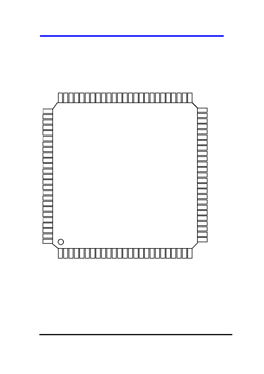
PACKAGE INFORMATION
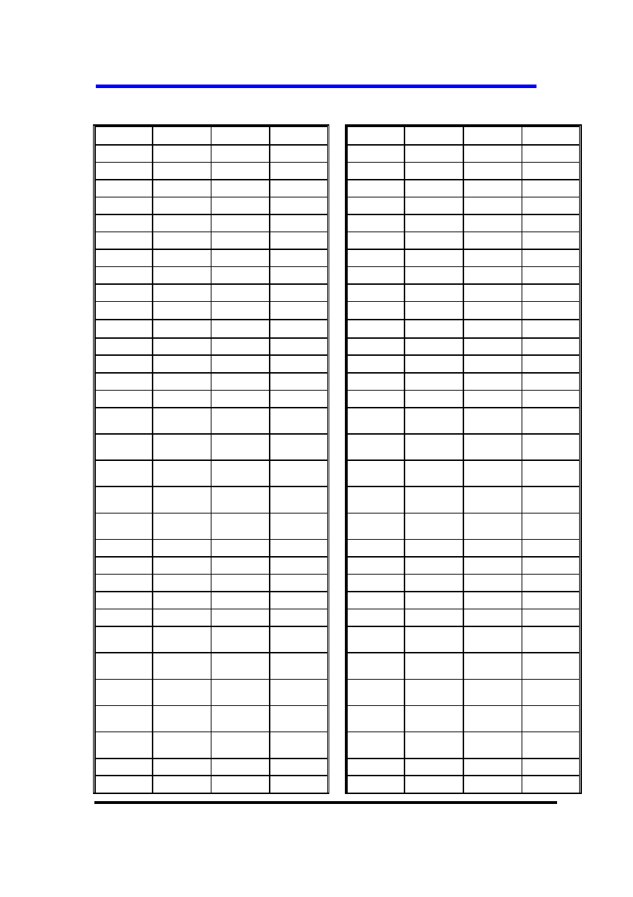
QFP
100QFP PACKAGE
52
53
54
55
SC1
SC2
SC3
SC4
SC5
57
58
59
SC6
SC7
SC8
SC9
SC10
62
63
64
65
SC11
SC12
SC13
SC14
SC15
67
68
69
SC16
SC17
SC18
SC19
SC20
72
73
74
75
SC21
SC22
SC23
SC24
SC25
77
78
79
80
SC26
SC27
SC28
SC29
SC30
29
28
27
26
SC80
SC79
SC78
SC77
SC76
24
23
22
21
SC75
SC74
SC73
SC72
SC71
19
18
17
16
SC70
SC69
SC68
SC67
SC66
14
13
12
11
SC65
SC64
SC63
SC62
SC61
9
8
7
6
SC60
SC59
SC58
SC57
SC56
4
3
2
1
SC55
SC54
SC53
SC52
SC51
50
D1_SID
CL2
AMS
CL1
ELB
45
SHL
VSS
D4_DR
D3_DM
D2_DL
49
48
47
46
44
43
42
41
40
V0
CS
M
D_OFF
VDD
35
ERB
VEE
V5
V43
V12
39
38
37
36
34
33
32
31
81
SC35
SC34
SC33
SC32
SC31
86
SC40
SC39
SC38
SC37
SC36
82
83
84
85
87
88
89
90
91
SC45
SC44
SC43
SC42
SC41
96
SC50
SC49
SC48
SC47
SC46
92
93
94
95
97
98
99
100
66
61
51
56
60
5
10
15
20
25
30
70
71
76
T66H0004A-Q
T66H0004A
TM Technology Inc. reserves the right P. 3 Publication Date: MAR. 2004
to change products or specifications without notice.
Revision:A
tm
TE
CH
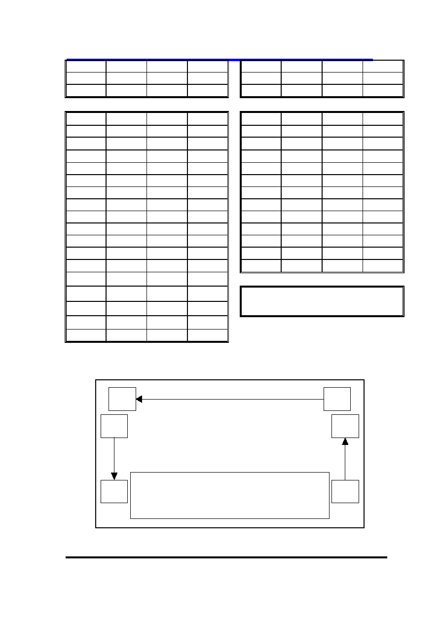
TQFP
100TQFP PACKAGE
52
53
54
55
SC78
SC79
57
58
59
62
63
64
65
67
68
69
72
73
74
75
24
23
22
21
SC52
SC51
SC50
SC49
SC48
19
18
17
16
SC47
SC46
SC45
SC44
SC43
14
13
12
11
SC42
SC41
SC40
SC39
SC38
9
8
7
6
SC37
SC36
SC35
SC34
SC33
4
3
2
1
SC32
SC31
SC30
SC29
SC28
50
D1_SID
CL2
AMS
CL1
ELB
45
SHL
VSS
D4_DR
D3_DM
D2_DL
49
48
47
46
44
43
42
41
40
D_OFF
VDD
35
ERB
VEE
39
38
37
36
34
33
32
31
81
SC12
SC11
SC10
SC9
SC8
86
SC17
SC16
SC15
SC14
SC13
82
83
84
85
87
88
89
90
91
SC22
SC21
SC20
SC19
SC18
96
SC27
SC26
SC25
SC24
SC23
92
93
94
95
97
98
99
100
66
61
51
56
60
5
10
15
20
25
70
71
T66H0004A-T
V0
CS
28
V5
V43
V12
30
29
27
26
76
SC7
SC6
SC5
SC4
SC3
77
78
79
80
SC53
SC54
SC55
SC56
SC57
SC58
SC59
SC60
SC61
SC62
SC63
SC64
SC65
SC66
SC67
SC68
SC69
SC70
SC71
SC72
SC73
SC74
SC75
SC76
SC77
SC1
SC2
SC80
M

T66H0004A
TM Technology Inc. reserves the right P. 4 Publication Date: MAR. 2004
to change products or specifications without notice.
Revision:A
tm
TE
CH
BLOCK DIAGRAM

T66H0004A
TM Technology Inc. reserves the right P. 5 Publication Date: MAR. 2004
to change products or specifications without notice.
Revision:A
tm
TE
CH
BLOCK DESCRIPTION
Name Function
COM/SEG
Clock control
Generates latch clock (LCK),shift clock(SCK) and control clock timing
according to the input of CL1,CL2 and control inputs(CS,AMS). In
common driver application mode, this block generates the shift clock
(LCK) for the common data Bi-directional shift register.
COM/SEG
Data latch
control
Determines the direction of segment data shift, and input data of each
Bi-directional shift register. In 4-bit segment data parallel transfer mode,
data is shifted by 4-bit unit. In common driver application mode, data is
transferred to the common data shift register directly, which disables this
block.
SEG
Power down
function
Controls the clock enable state of the current driver according to the
input value of enable pin (ELB or ERB). If enable input value is "Low",
every clock of the current driver is enabled and the clock control block
works. But if enable input is "High", current driver is disabled and the
input data value has no effect on the output level. So power consumption
can be lowered.
SEG
Output level
selector
Controls the output voltage level according to the input control pin (M
and DISPOFFB) (refer to PIN DESCRIPTION).
COM/SEG
20x4-bit
segment data
Bi-directional
shift register
Stores output data value by shifting the input values. In 1-bit serial
interface mode application, all 80 shift clocks (SCK) are needed to store
all the display data. But in 4-bit parallel transfer mode application, only
20 clocks are needed. In common driver application mode, this block
does not work.
SEG
80�bit data
latch/common
data
Bi-directional
shift register
In segment driver application mode, the data from the 20x4-bit segment
data shift register are latched for segment driver output. In single-type
common driver application, 1-bit input data (from DL or DR pin) is
shifted and latched by the direction according to the SHL signal input. In
dual-type common application mode, 80-bit registers are divided by two
blocks and controlled independently (refer to NOTE 3).
COM/SEG
80-bit level
shifter
Voltage level shifter block for high voltage part. The inputs of this block
are of logical voltage level and the outputs of this block are at high
voltage level value. These values are output to the driver.
SEG
80-bit 4-level
driver
Selects the output voltage level according to M and latched data value. If
the data value is "High" the driver output is at selected voltage level (V0
or V5), and in the reverse case the driver output value is at the
non-selected level (V12 or V43). In segment driver application mode,
non-selected output value is V2 or V3. And when in common driver
application, this value becomes V1 or V4.
SEG

T66H0004A
TM Technology Inc. reserves the right P. 6 Publication Date: MAR. 2004
to change products or specifications without notice.
Revision:A
tm
TE
CH
PIN DESCRIPTION
Pin I/O Name
Function
Interface
V
DD
Logical "High" input port(+5V�10%,+3V�10%)
Vss 0V(GND)
V
EE
Power
supply
Logical "Low" for high voltage part
Power
V0,V12,
V43,V5
I
LCD driver
output voltage
level
Bias supply voltage input to drive the LCD. Bias
voltage divided by the resistance is usually used as a
supply voltage source (refer to NOTE 2).
Power
SC1-SC80 O
LCD driver
output
Display data output pin which corresponds to the
respective latch contents. One of V0, V12, V34 and V5
is selected as a display driving voltage source
according to the combination of the latch data level
and M signal (refer to NOTE 1).
LCD
CL2 I
Data shift
clock
Clock pulse input for the bi-directional shift register.
- In segment driver application mode, the data is
shifted to 20x4-bit segment data shift.
The clock pulse, which was input when the enable bit
(ELB/ERB) is in not active condition, is invalid.
- In common driver application mode, the data is
shifted to 80-bit common data bi-directional shift
register by the CL1 clock.
Hence, this clock pin is not used (Open or connect this
pin to VDD).
Controller
M I
AC signal for
LCD driver
output
Alternate signal input pin for LCD driving.
Normal frame inversion signal is input in to this pin.
Controller
CL1 I
Data latch
clock
- In segment driver application mode, this signal is
used for latching the shift register contents at the
falling edge of this clock pulse.
CL1 pulse "High" level initializes power-down
function block.
- In common driver application mode, CL1 is used as a
shifting clock of common output data.
Controller
DISPOFFB I
Display OFF
control
Control input pin to fix the driver output (SC1-SC80)
to V0 level, during "Low" value input. LCD becomes
non-selected by V0 level output from every output of
segment drivers and every output of common drivers.
Controller
CS I
COM/SEG
mode control
When CS = "Low", T66H0004A is used as an 80-bit
segment driver.
When CS = "High", T66H0004A is set to an 80-bit
common driver.
VDD/VSS
According to the input value of the AMS and the CS
pin, application mode of T66H0004A is differs as
shown below.
CS AMS
Application mode
0 0
4-bit parallel interface mode
0 1
1-bit serial interface mode
SEG
1 0
Single type application mode
AMS I
Application
mode select
1 1
Dual type application mode
COM
VDD/VSS
D1_SID,
D2_DL,
I/O
Display data
input/serial
- In segment driver application mode, these pins are
used as 4-bit data input pin (when 4-bit parallel
Controller

T66H0004A
TM Technology Inc. reserves the right P. 7 Publication Date: MAR. 2004
to change products or specifications without notice.
Revision:A
tm
TE
CH
D3_DM,
D4_DR
input data/left,
right data
input output
interface mode: AMS = "Low"), or D1_SID is used as
serial data input pin and other pins are not used
(connect these to VDD) (when 1-bit serial interface
mode: AMS = "High").
- In common driver application mode, the data is
shifted from D2_DL(D4_DR) to D4_DR
(D2_DL),when in single type interface mode
(AMS = "Low"). In dual-type application case, the
data are shifted from D2_DL and D3_DM (D4_DR
and D3_DM) to D4_DR(D2_DL). In each case the
direction of the data shift and the connection of data
pins are determined by SHL input (refer to NOTE3,
NOTE4).
SHL Input
Shift direction
control
When SHL = "Low", data is shifted from left to right.
When SHL = "High", the direction is reversed.(refer to
NOTE3)
VDD/VSS
- In segment driver application mode, the internal
operation is enabled only when enable input (ELB or
ERB) is "Low" (power down function). When several
drivers are serially connected, the enable state of each
driver is shifted according to the SHL input. Connect
these pins as below.
Segment Driver
SHL
ELB ERB
L Output(open)
Input(VSS)
H Input(VSS)
Output(open)
ELB,ERB I/O
Enable data
input/output
- In common driver application mode, power down
function is not used.
Open these pins.

T66H0004A
TM Technology Inc. reserves the right P. 8 Publication Date: MAR. 2004
to change products or specifications without notice.
Revision:A
tm
TE
CH
NOTE 1. Output Level Control
Output level(SC1-SC80)
M Latched
data
DISPOFFB
SEG Mode
COM Mode
L L H
V12(V2)
V12(V1)
L H H V0
V5
H L H
V43(V3)
V43(V4)
H H H V5 V0
X X L V0 V0
NOTE 2. LCD Driving Voltage Application Circuit
(1) Segment driver application(CS = "Low")
(2) Common driver application(CS = "High")

T66H0004A
TM Technology Inc. reserves the right P. 9 Publication Date: MAR. 2004
to change products or specifications without notice.
Revision:A
tm
TE
CH
NOTE 3. Data Shift Direction according to Control Signals
(1) When CS = "Low"(Segment driver application)
AMS SHL Application
mode
Data Direction
Input Pin
L
Shift Direction
last data first
data
s
c
1
s
c
2
s
c
3
s
c
4
s
c
7
3
s
c
7
4
s
c
7
5
s
c
7
6
s
c
7
7
s
c
7
8
s
c
7
9
s
c
8
0
D D D D D D D D
D
1
D
2
D
3
D
4
1 2 3 4 1 2 3 4
L
H
4-Bit Parallel
Data Transfer
Mode(SEG)
Shift Direction
first data
last data
s
c
1
s
c
2
s
c
3
s
c
4
s
c
7
3
s
c
7
4
s
c
7
5
s
c
7
6
s
c
7
7
s
c
7
8
s
c
7
9
s
c
8
0
D D D D D D D D
D
4
D
3
D
2
D
1
4 3 2 1 4 3 2 1
D1_SID,
D2_DL,
D3_DM,
D4_DR
L
Shift Direction
last data (D1_SID) first
data
s
c
1
s
c
2
s
c
3
s
c
4
s
c
7
3
s
c
7
4
s
c
7
5
s
c
7
6
s
c
7
7
s
c
7
8
s
c
7
9
s
c
8
0
H
H
1-Bit Serial
Data Transfer
Mode (SEG)
Shift Direction
first data last data
s
c
1
s
c
2
s
c
3
s
c
4
s
c
7
3
s
c
7
4
s
c
7
5
s
c
7
6
s
c
7
7
s
c
7
8
s
c
7
9
s
c
8
0
D1_SID
D1
D2
D3
D4
D1
D2
D3
D4

T66H0004A
TM Technology Inc. reserves the right P. 10 Publication Date: MAR. 2004
to change products or specifications without notice.
Revision:A
tm
TE
CH
(2) When CS = "High"(common driver application)
AMS SHL Application
mode
Data Direction
Input Pin
L
Shift Direction
S
C
1
S
C
2
S
C
3
S
C
3
8
S
C
3
9
S
C
4
0
S
C
4
1
S
C
4
2
S
C
4
3
S
C
7
8
S
C
7
9
S
C
8
0
D2_DL
L
H
Single-type
Application
Mode
(COM)
Shift Direction
S
C
1
S
C
2
S
C
3
S
C
3
8
S
C
3
9
S
C
4
0
S
C
4
1
S
C
4
2
S
C
4
3
S
C
7
8
S
C
7
9
S
C
8
0
D4_DR
L
Shift Direction
S
C
1
S
C
2
S
C
3
S
C
3
8
S
C
3
9
S
C
4
0
S
C
4
1
S
C
4
2
S
C
4
3
S
C
7
8
S
C
7
9
S
C
8
0
D2_DL,
D3_DM
H
H
Dual-type
Application
Mode
(COM)
Shift Direction
S
C
1
S
C
2
S
C
3
S
C
3
8
S
C
3
9
S
C
4
0
S
C
4
1
S
C
4
2
S
C
4
3
S
C
7
8
S
C
7
9
S
C
8
0
D4_DR,
D3_DM
Input Data
(D2 DL)
Output Data
(D4_DR)
Input Data
(D4 DR)
Output Data
(D2_DL)
Input Data 1
(D2_DL)
Output Data
(D4_DR)
Input Data 2
(D3_DM)
Input Data 1
(D4_DR)
Output Data
(D2_DL)
Input Data 2
(D3_DM)

T66H0004A
TM Technology Inc. reserves the right P. 11 Publication Date: MAR. 2004
to change products or specifications without notice.
Revision:A
tm
TE
CH
NOTE 4. Usage of Data Pins
Data interface pin
COM/SEG
(CS pin)
Application mode
(AMS pin)
SHL
D1_SID D2_DL D3_DM D4_DR
4-bit parallel interface
mode(AMS = "Low")
X D1(input)
D2(input2)
D3(input3)
D4(input4)
SEG
(CS = "Low") 1-bit serial interface
mode (AMS = "High")
X
SID(input)
Connect to VDD
L DL(input)
DR(output)
Single-type application
mode( AMS = "Low")
H
Open
DL(output)
Open
DR(input)
L DL(input1)
DM(input2)
DR(output2)
COM
(CS = "High") Dual-type application
mode (AMS = "high")
H
Open
DL(output2) DM(input2) DR(input1)
MAXIMUM ABSOLUTE LIMIT
Characteristic Symbol
Value
Unit
Power supply voltage
VDD
-0.3 to +7.0
Driver supply voltage
Vlcd
0 to +30
Input voltage
Vin
-0.3 to
VDD+0.3
V
Operating temperature
Topr
-30 to +85
Storage temperature
Tstg
-55 to +150
�
*NOTE: Voltage greater than above may do damage to the circuit.

T66H0004A
TM Technology Inc. reserves the right P. 12 Publication Date: MAR. 2004
to change products or specifications without notice.
Revision:A
tm
TE
CH
ELECTRICAL CHARACTERISTICS
DC CHARACTERISTICS
(1)
Segment Driver Applicatio
n
(Vss = 0V, Ta=-30 to +85
0
C)
Characteristic Symbol Test
Condition Min.
Typ.
Max.
Unit
V
DD
-
2.7 - 5.5
Operating Voltage 1
V
LCD
V
IN
= V
DD
�V
EE
6
-
28
V
IH
- 0.8V
DD
- V
DD
Input voltage (1)
V
I L
- 0
-
0.2
V
DD
V
V
OH
I
OH
= -0.4mA
V
DD
-0.4 -
-
Output voltage (2)
V
OL
I
OL
= 0.4mA
-
-
0.4
V
Input leakage current 1 (1)
I
IL1
V
IN
= V
DD
to Vss
-10
-
10
Input leakage current 2 (3)
I
IL2
V
IN
= V
DD
to V
EE
-25
-
25
uA
On resistance (4)
R
ON
I
ON
= 100uA
-
2
4
K
Ohm
I
STBY
F
CL1
=32 KHz
M=Vss
Vss pin
-
-
50
uA
V
DD
= 5V
-
-
5
I
DD
V
DD
= 3V
-
-
2
mA
Supply current (5)
I
EE
F
CL1
= 32KHz
F
M
= 80Hz
V
DD
=5V
-
-
500
uA
NOTES:
1. Applied to Cl1,CL2,ELB,ERB,D1_SID-D4_DR,SHL,DISPOFFB,M,CS,AMS pin
2. ELB,ERB pin
3. V0,V12,V43,V5 pin
4. V
LCD
= V
DD
-V
EE
, V0=V
DD
=5V, V5=V
EE
=-23V
V12 = V
DD
-2/n(V
LCD
), V43= V
EE
+2/n(V
LCD
), n=17(1/256 duty,1/17 bias)
5. V0= V
DD
, V12=1.71V(V
DD
=5V) or �0.06V(V
DD
=3V)
V43=-19.71V(V
DD
=5V) or �19.94V(V
DD
=3V), V5=V
EE
=-23V, no-load condition (1/256 duty,1/17 bias)
4-bit parallel interface mode.
Istby: V
DD
=5V, CL2=Vss, SHL=Vss, DISPOFFB= V
DD
, M = Vss, display data pattern=0000
I
DD
: V
DD
=3V, f
CL2
=4MHz, display data pattern=0101
V
DD
= 5V, f
CL2
f
CL2
=5.12MHz, display data pattern=0101
I
EE
: V
DD
=5V, f
CL2
=5.12MHz, display data pattern=0101, V
EE
pin

T66H0004A
TM Technology Inc. reserves the right P. 13 Publication Date: MAR. 2004
to change products or specifications without notice.
Revision:A
tm
TE
CH
ELECTRICAL CHARACTERISTICS
(2) Common Driver Application
(Vss = 0V, Ta=-30 to +85
0
C)
Characteristic Symbol Test
Condition Min.
Typ.
Max.
Unit
V
DD
-
2.7 - 5.5
Operating Voltage
V
LCD
V
IN
= V
DD
�V
EE
6
-
28
V
IH
- 0.8
V
DD
- V
DD
Input voltage (1)
V
IL
- 0
-
0.2
V
DD
V
V
OH
I
OH
= -0.4mA
V
DD
-0.4
-
-
Output voltage (3)
V
OL
I
OL
= 0.4mA
-
-
0.4
V
Input leakage current 1 (1)
I
IL1
V
IN
= V
DD
to Vss
-10
-
10
Input leakage current 2 (2)
I
IL2
V
IN
=0, V
DD
=5V(PULL UP)
-50
-125
-250
Input leakage current 3 (4)
I
IL3
V
IN
= V
DD
to V
EE
-25
-
25
uA
On resistance (5)
R
ON
I
ON
= 100uA
-
2
4
K
Ohm
I
STBY
F
CL1
=32KHz Vss
pin
-
-
50
V
DD
=5V
-
-
200
I
DD
V
DD
=3V
-
-
120
Supply current(6)
I
EE
F
CL1
=32KHz
F
M
=80Hz
V
DD
=5V
-
-
150
uA
NOTES:
1. Applied to CL1, D2_DL (SHL=LOW), D4_DR (SHL=HIGH), SHL, DISPOFFB, M, CS, AMS pin.
2. Pull-up input pins: CL2, D1_SID, D3_DM (AMS=HIGH), ELB (SHL=LOW), ERB (SHL= HIGH).
3. D2_DL (SHL = HIGH), D4_DR (SHL = LOW) pin.
4. V0, V12, V43, V5 pin
5. V
LCD
= V
DD
-V
EE
, V0= V
DD
=5V,V5=V
EE
=-23V
V12 = V
DD
-1/n(V
LCD
), V43= V
EE
+1/n(V
LCD
), n=17(1/256 duty, 1/17 bias)
6. V0= V
DD
, V12=3.35V(V
DD
=5V) or 1.47V(V
DD
=3V),
V43=-21.35V(V
DD
=5V) or �21.47V(V
DD
=3V), V5= V
EE
=-23V, no-load condition (1/256 duty,
1/17 bias)Single-type mode operation: AMS = Vss, SHL = Vss,
DISPOFFB = V
DD
D1_SID=D3_DM=VDD, D4_DR=OPEN, ELB+ERB+OPEN,
I
STBY
: V
DD
=5V, M=Vss, D2_DL=Vss
I
DD
: f
M
=80Hz, D2_DL= V
DD
V
DD
=3V, display data pattern=10000000...,01000000...,00100000...,00010000...,...
V
DD
=5V.displat data pattern=10000000...,01000000...,00100000...,00010000...,...
I
EE
: f
M
=80Hz,D2_DL= V
DD
V
DD
=5V, current through V
EE
pin, display data
pattern=100000000...,01000000...,00100000...,00010000...,...

T66H0004A
TM Technology Inc. reserves the right P. 14 Publication Date: MAR. 2004
to change products or specifications without notice.
Revision:A
tm
TE
CH
AC CHARACTERRISTICS
(1) Segment Driver Application
(Vss = 0V, Ta=-30 to +85
0
C)
(1) VDD=5V�10% (2) VDD=3V�10%
Characteristic Symbol
Test
Condition
Min. Typ. Max. Min. Typ. Max.
Unit
Clock cycle time
t
cy
Duty=50% 125 - - 250 - -
Clock pulse width
t
wck
- 45
-
-
95
-
-
Clock rise/fall time
t
R
/
t
F
- -
-
30
-
-
30
Data set-up time
t
DS
- 30
-
-
65
-
-
Data hold time
t
DH
- 30
-
-
65
-
-
Clock set-up time
t
cs
- 80
-
-
120
-
-
Clock hold time
t
ch
- 80
-
-
120
-
-
ELB Output
60
125
Propagation delay
time
t
phl
ERB Output
- -
60
- -
125
ELB Input
30
65
ELB,ERB set-up time t
psu
ERB Input
30
- -
65
- -
ns
DISPOFFB low pulse
width
t
WDL
- 1.2
-
-
1.2
-
-
us
DISPOFFB clear
time
t
cd
- 100
-
-
100
-
ns
M-OUT propagation
delay time
t
pd1
- - 1.0
- -
1.2
CL1-OUT
propagation delay
time
t
pd2
- - 1.0
- -
1.2
DISPOFFB-OUT
propagation delay
time
t
pd3
C
L
=15pF
- - 1.0
- -
1.2
us
Latch pulse rise to
Shift clock rise time
t
LS
80
-
-
120
-
-
ns

T66H0004A
TM Technology Inc. reserves the right P. 15 Publication Date: MAR. 2004
to change products or specifications without notice.
Revision:A
tm
TE
CH
AC CHARACTERISTICS
(2) Common Driver Application
(Vss = 0V, Ta=-30 to +85
0
C)
(1) VDD=5V�10% (2) VDD=3V�10%
Characteristic Symbol
Test
Condition
Min. Typ. Max. Min. Typ. Max.
Unit
Clock cycle time
t
cy
Duty=50% 250 - - 500 - -
Clock pulse width
t
wck
- 45
-
-
95
-
-
Clock rise/fall time
t
R/
t
F
- -
-
50
-
-
50
Data set-up time
t
DS
- 30
-
-
65
-
-
Data hold time
t
DH
- 30
-
-
65
-
-
ns
DISPOFFB low pulse
width
t
wdl
- 1.2
-
-
1.2
-
-
us
DISPOFFB clear
time
t
cd
- 100
-
-
100
-
Output delay time
t
dl
- -
200
- -
250
ns
M-OUT propagation
delay time
t
pd1
- - 1.0
- -
1.2
CL1-OUT
propagation delay
time
t
pd2
- - 1.0
- -
1.2
DISPOFFB-OUT
propagation delay
time
t
pd3
C
L
=15pF
- - 1.0
- -
1.2
us

T66H0004A
TM Technology Inc. reserves the right P. 16 Publication Date: MAR. 2004
to change products or specifications without notice.
Revision:A
tm
TE
CH
AC CHARACTERISTICS
(3) Segment Driver Application Timing

T66H0004A
TM Technology Inc. reserves the right P. 17 Publication Date: MAR. 2004
to change products or specifications without notice.
Revision:A
tm
TE
CH
AC CHARACTERISTICS
(4) Common Driver Application Timing

T66H0004A
TM Technology Inc. reserves the right P. 18 Publication Date: MAR. 2004
to change products or specifications without notice.
Revision:A
tm
TE
CH
POWER DOWN FUNCTION
In the case of cascade connection of segment mode drivers,T66H0004A has a "power
down function" In order to reduce the power consumption.
SHL Enable input Enable output
Current driver status
The other drivers status
L ERB
ELB
While ERB = "Low", current
driver is enabled.
Disabled
H ELB
ERB
While ELB = "Low", current
driver is enabled
Disabled
* In the case of common driver application, power down function dose not work.
T66H0004A
TM Technology Inc. reserves the right P. 19 Publication Date: MAR. 2004
to change products or specifications without notice.
Revision:A
tm
TE
CH
OPERATION TIMING DIAGRAM
(1) 4-bit Parallel Mode Interface Segment Driver
! When SHL = "High"
! When SHL = "Low"

T66H0004A
TM Technology Inc. reserves the right P. 20 Publication Date: MAR. 2004
to change products or specifications without notice.
Revision:A
tm
TE
CH
(2) 1-bit Serial Mode Interface Segment Driver
! When SHL = High"
! When SHL = "Low"

T66H0004A
TM Technology Inc. reserves the right P. 21 Publication Date: MAR. 2004
to change products or specifications without notice.
Revision:A
tm
TE
CH
(3) Single-type Interface Mode Common Driver
! When SHL = "Low"
! When SHL = "High"

T66H0004A
TM Technology Inc. reserves the right P. 22 Publication Date: MAR. 2004
to change products or specifications without notice.
Revision:A
tm
TE
CH
(4) DUAL-type Interface Mode Common Driver
! When SHL = "Low"
! When SHL = "High"

T66H0004A
TM Technology Inc. reserves the right P. 23 Publication Date: MAR. 2004
to change products or specifications without notice.
Revision:A
tm
TE
CH
(5) Common/Segment driver Timing(1/200 DUTY)

T66H0004A
TM Technology Inc. reserves the right P. 24 Publication Date: MAR. 2004
to change products or specifications without notice.
Revision:A
tm
TE
CH
APPLICATION INFORMATION
1-bit Serial Interface Mode (80 output Segment Driver)
(a) Lower View(SHL = L , AMS = H )
(b)Upper View (SHL = H, AMS = H)

T66H0004A
TM Technology Inc. reserves the right P. 25 Publication Date: MAR. 2004
to change products or specifications without notice.
Revision:A
tm
TE
CH
4-bit Parallel Interface Mode (80 output Segment Driver)
(a) Lower View(SHL = L , AMS = L)
(b) Upper View (SHL = H , AMS = L)

T66H0004A
TM Technology Inc. reserves the right P. 26 Publication Date: MAR. 2004
to change products or specifications without notice.
Revision:A
tm
TE
CH
Single-type Interface Mode (80 output Common Driver)

T66H0004A
TM Technology Inc. reserves the right P. 27 Publication Date: MAR. 2004
to change products or specifications without notice.
Revision:A
tm
TE
CH
Dual-type Interface Mode (40 output Common Driver)
NOTE:
Using this application mode (dual-type common mode), the duty ratio can be reduced to half.
In case, 1/200 duty can be used to drive the 400 common LCD panel.

T66H0004A
TM Technology Inc. reserves the right P. 28 Publication Date: MAR. 2004
to change products or specifications without notice.
Revision:A
tm
TE
CH
APPLICATION CIRCUIT EXAMPLE

T66H0004A
TM Technology Inc. reserves the right P. 29 Publication Date: MAR. 2004
to change products or specifications without notice.
Revision:A
tm
TE
CH
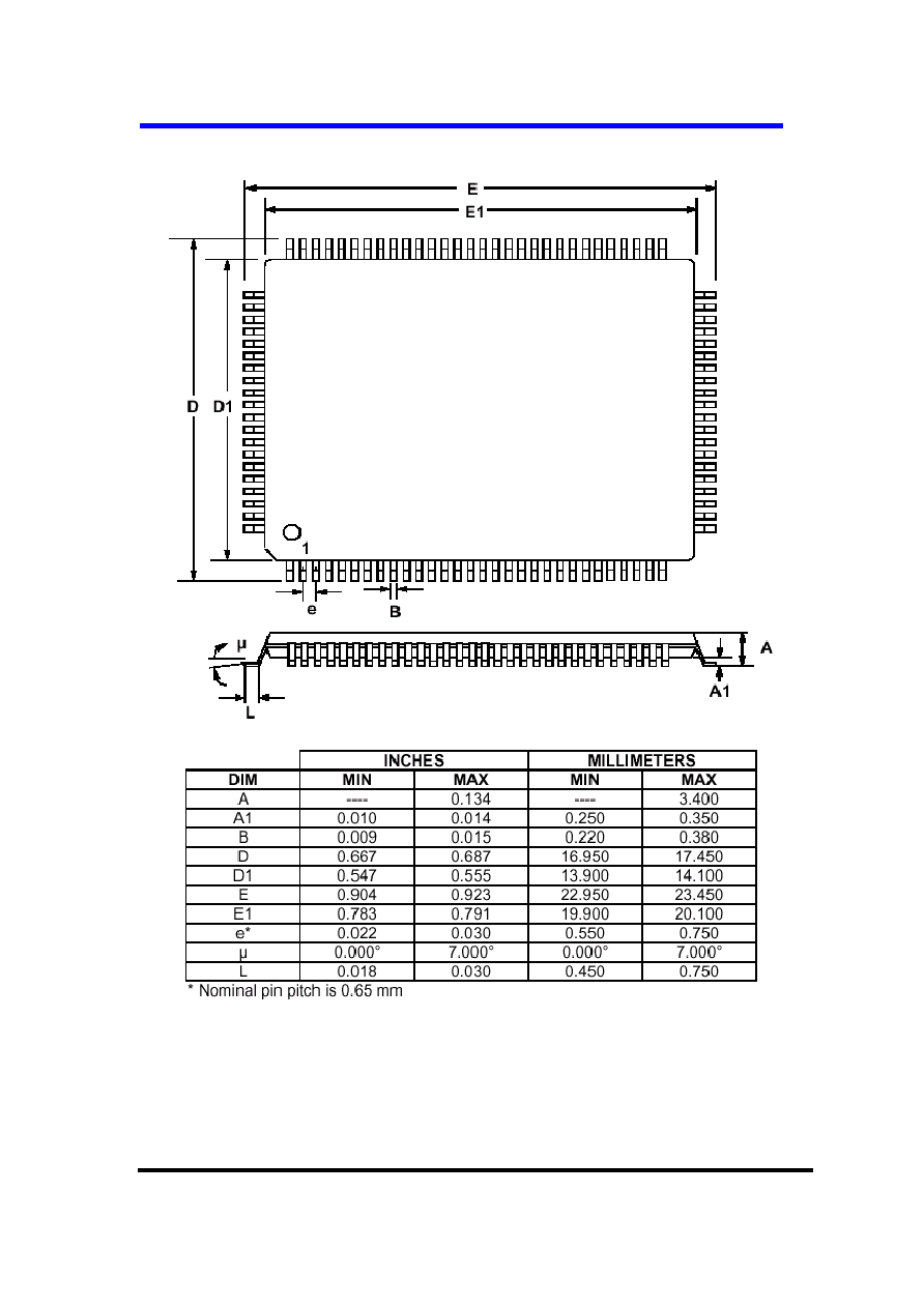
PACKAGE DIMENSION
(Unit: mm)
100 pin TQFP
T66H0004A
TM Technology Inc. reserves the right P. 30 Publication Date: MAR. 2004
to change products or specifications without notice.
Revision:A
tm
TE
CH
100 pin QFP
T66H0004A
TM Technology Inc. reserves the right P. 31 Publication Date: MAR. 2004
to change products or specifications without notice.
Revision:A
tm
TE
CH
Pad List(For T66H0004A1S use)
Pad No. Pin Name
X
Y
Pad No. Pin Name
X
Y
1
Y51
-1127.2 1473.25
36
VOP:P
-449.75 -1534.4
2
Y52
-1127.2 1373.25
37
CS
-349.75 -1534.4
3
Y53
-1127.2 1273.25
38
M
-249.75 -1534.4
4
Y54
-1127.2 1173.25
39
DISSPO
-149.75 -1534.4
5
Y55
-1127.2 1073.25
40
VDD
-49.75 -1534.4
6
Y56
-1127.2 973.25
41
SHL
50.25 -1534.4
7
Y57
-1127.2 873.25
42
VSS
150.25 -1534.4
8
Y58
-1127.2 773.25
43
D4_DR
250.25 -1534.4
9
Y59
-1127.2 673.25
44
D3_DM
350.25 -1534.4
10
Y60
-1127.2 573.25
45
D2_DL
450.25 -1534.4
11
Y61
-1127.2 473.25
46
D1_SID
550.25 -1534.4
12
Y62
-1127.2 373.25
47
CL2
650.25 -1534.4
13
Y63
-1127.2 273.25
48
AMS
750.25 -1534.4
14
Y64
-1127.2 173.25
49
CL1
850.25 -1534.4
15
Y65
-1127.2 73.25
50
ELB
950.25 -1534.4
16
Y66
-1127.2 -26.75
51
Y1
1127.7 -1426.7
5
17
Y67
-1127.2 -126.75
52
Y2
1127.7 -1326.7
5
18
Y68
-1127.2 -226.75
53
Y3
1127.7 -1226.7
5
19
Y69
-1127.2 -326.75
54
Y4
1127.7 -1126.7
5
20
Y70
-1127.2 -426.75
55
Y5
1127.7 -1026.7
5
21
Y71
-1127.2 -526.75
56
Y6
1127.7 -926.75
22
Y72
-1127.2 -626.75
57
Y7
1127.7 -826.75
23
Y73
-1127.2 -726.75
58
Y8
1127.7 -726.75
24
Y74
-1127.2 -826.75
59
Y9
1127.7 -626.75
25
Y75
-1127.2 -926.75
60
Y10
1127.7 -526.75
26
Y76
-1127.2 -1026.7
5
61
Y11
1127.7 -426.75
27
Y77
-1127.2 -1126.7
5
62
Y12
1127.7 -326.75
28
Y78
-1127.2 -1226.7
5
63
Y13
1127.7 -226.75
29
Y79
-1127.2 -1326.7
5
64
Y14
1127.7 -126.75
30
Y80
-1127.2 -1426.7
5
65
Y15
1127.7 -26.75
31
ERB
-949.75 -1534.4
66
Y16
1127.7 73.25
32
VEEP:G
-849.75 -1534.4
67
Y17
1127.7 173.25
T66H0004A
TM Technology Inc. reserves the right P. 32 Publication Date: MAR. 2004
to change products or specifications without notice.
Revision:A
tm
TE
CH
33
V5P
-749.75 -1534.4
68
Y18
1127.7 273.25
34
V43P
-649.75 -1534.4
69
Y19
1127.7 373.25
35
V12P
-549.75 -1534.4
70
Y20
1127.7 473.25
Pad No. Pin Name
X
Y
88
Y38
250.25 1534.4
71
Y21
1127.7 573.25
89
Y39
150.25 1534.4
72
Y22
1127.7 673.25
90
Y40
50.25 1534.4
73
Y23
1127.7 773.25
91
Y41
-49.75 1534.4
74
Y24
1127.7 873.25
92
Y42
-149.75 1534.4
75
Y25
1127.7 973.25
93
Y43
-249.75 1534.4
76
Y26
1127.7 1073.25
94
Y44
-349.75 1534.4
77
Y27
1127.7 1173.25
95
Y45
-449.75 1534.4
78
Y28
1127.7 1273.25
96
Y46
-549.75 1534.4
79
Y29
1127.7 1373.25
97
Y47
-649.75 1534.4
80
Y30
1127.7 1473.25
98
Y48
-749.75 1534.4
81
Y31
950.25 1534.4
99
Y49
-849.75 1534.4
82
Y32
850.25 1534.4
100
Y50
-949.75 1534.4
83
Y33
750.25 1534.4
84
Y34
650.25 1534.4
CHIP SIZE ==>
85
Y35
550.25 1534.4
( 2349.4,3163.8 )
86
Y36
450.25 1534.4
87
Y37
350.25 1534.4
Y31
Y50
Y51
Y80
Y30
Y1
ELB
CL1
AMS
CL2
D1_SID
D2_DL
D3_DM
D4_DR
VSS
SHL
VDD
DISPOFF
M
CS
V0
V12
V43
V5
VEE
ERB
T66H0004A1S