
TE
CH
tm
T81L0003A
TM Technology, Inc. reserves the right P. 1
Publication Date: SEP. 2004
to change products or specifications without notice. Revision: C
MCU
Reduced I/O 8-bit MCU
FEATURES
! Compatible with MCS-51 Products
! 128 x8 bit RAM
! Embedded 8k X 8 bit data OTP ROM
! 13 bi-direction I/O Lines.
! System clock: Typ. 12MHz @ 2.5 ~ 5.5V.
! 2 External Interrupt Input
! Programmable Serial UART Channel.
! Watch Dog Timer
! One 16-bit Timer/Counter (T0) & Two 16-bit Timer (T1, T2)
! On-chip selectable crystal driving PAD or RC oscillator.
! Low Power and wake-able power down mode
! One Buzzer Driving Pad.P1.0 (driving capability up to 40mA).
! SOP18/DIP18 Package.
! Typical 3.3V Operating Voltage.
Description
The T81L0003A is a low voltage and low cost and reduced I/O 8-bit high performance 8051-like
MCU. The T81L0003A provides 13 bi-direction I/Os for end user programming with other device and
3 timers (but only one counter) for more applications and low cost.
Part Number Example
Part No.
Pkg.
Description
T81L0003A-AK
DIP 18 pin
RC oscillation
T81L0003A-AD
SOP 18 pin
RC oscillation
T81L0003A-BK
DIP 18 pin
Crystal oscillation
T81L0003A-BD
SOP 18 pin
Crystal oscillation
TE
CH
tm
T81L0003A
TM Technology, Inc. reserves the right P. 2
Publication Date: SEP. 2004
to change products or specifications without notice. Revision: C
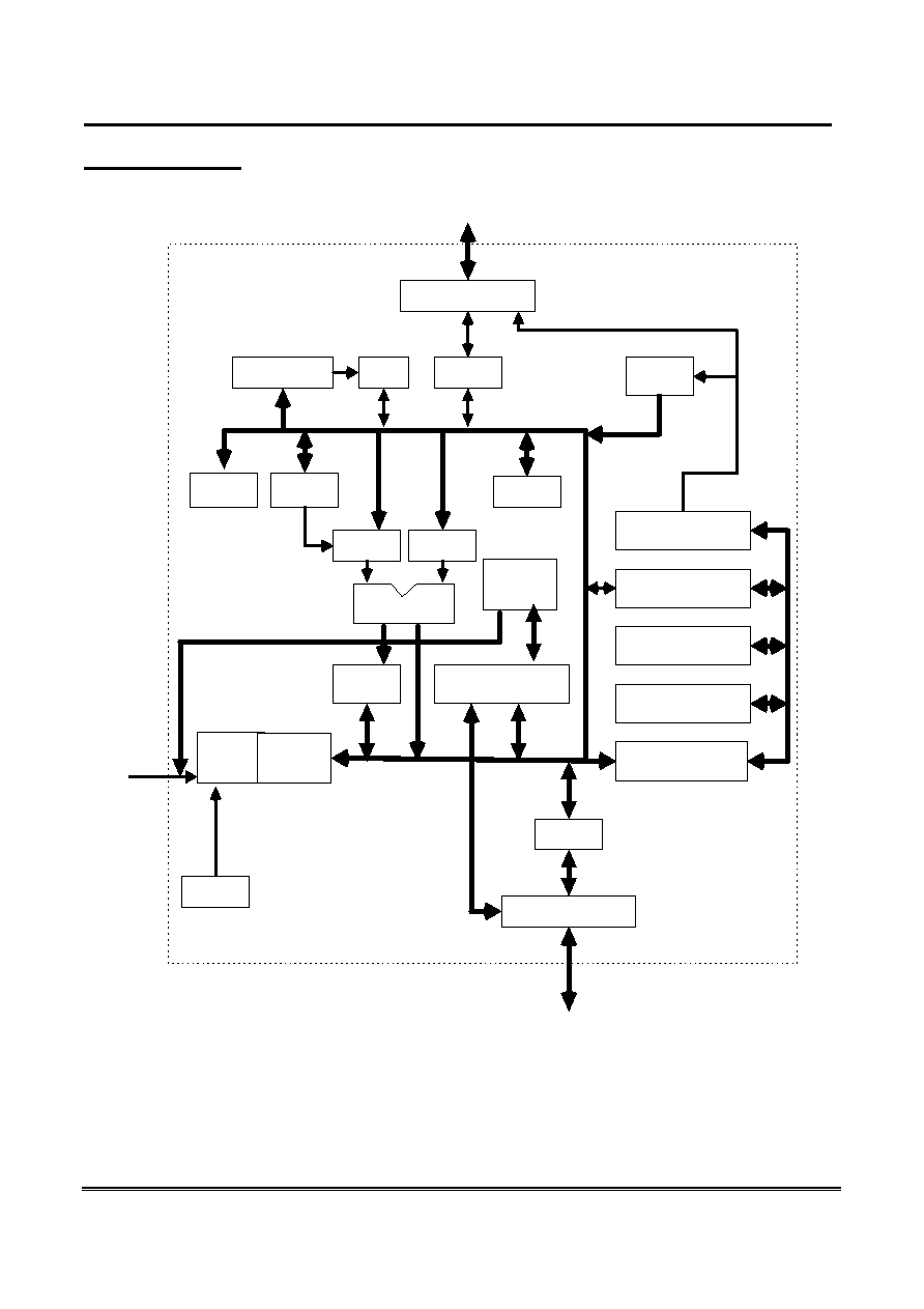
Block Diagram
Port 1 Drivers
RAM Addr.
Register
RAM
Port 1
Latch
OTP
ROM
B
Register
ACC
Stack
Pointer
TMP2
TMP1
ALU
PSW
Interrupt, Serial port,
and Timer Block
Timing &
Control
Instruction
Register
Port 3
Latch
Port 3 Drivers
Program Address
Register
Buffer
PC Incrementer
Program Counter
DPTR
P1.0 -P1.7
P3.0 -P3.4
RST
OSC
WDT
TE
CH
tm
T81L0003A
TM Technology, Inc. reserves the right P. 3
Publication Date: SEP. 2004
to change products or specifications without notice. Revision: C
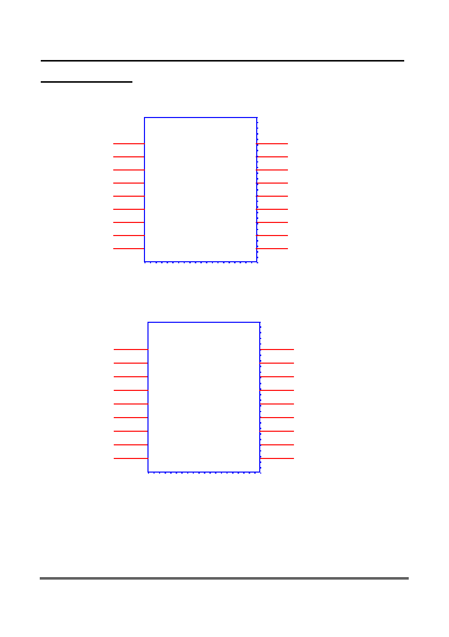
Pin Configuration
P1.3
15
VDD
2
VSS
7
P1.5
17
P1.0/BUZ
12
P3.1/TXD
4
P3.3/INT1
9
P1.2
14
T81L0003A-AK, AD
P1.6
18
OSCR
5
P1.7
1
P1.4
16
P3.2/INT0
11
P3.0/RXD
8
RST
3
P1.1
13
STOP
6
P3.4/T0
10
P3.2/INT0
11
RST
3
P1.2
14
P3.0/RXD
8
T81L0003A-BK,BD
P1.4
16
P3.4/T0
10
XIN
6
VDD
2
P1.6
18
P1.1
13
VSS
7
P3.1/TXD
4
P3.3/INT1
9
P1.3
15
P1.7
1
XOUT
5
P1.5
17
P1.0/BUZ
12

TE
CH
tm
T81L0003A
TM Technology, Inc. reserves the right P. 4
Publication Date: SEP. 2004
to change products or specifications without notice. Revision: C
Pin Assignment
Pin No. .Assignment
I/O
Options
Description
1
P1.7
I/O
General Purpose I/O
2 VDD -- 3.3V
Power Supply
3 RST I
Reset signal input
4 P3.1/TXD
I/O
General Purpose I/O and serial transmit
5(BK, BD)
XOUT
O
Crystal output terminal
5(AK, AD)
OSCR
I
RC Input
6(BK, BD)
XIN
I
Crystal input terminal
6(AK, AD)
STOP
O
RC Stop
7 VSS --
GND
Ground
8 P3.0/RXD
I/O
General Purpose I/O and serial receive
9 P3.3/INT1
I/O
General Purpose I/O and interrupt1 input
10
P3.4/T0
I/O
General Purpose I/O and Timer0
11 P3.2/INT0
I/O
General Purpose I/O and interrupt0 input
12 P1.0/BUZ
I/O
General Purpose I/O and Buzzer driving pad
13 P1.1
I/O
General Purpose I/O
14
P1.2
I/O
General Purpose I/O
15
P1.3
I/O
General Purpose I/O
16 P1.4
I/O
General Purpose I/O
17 P1.5
I/O
General Purpose I/O
18 P1.6
I/O
General Purpose I/O

TE
CH
tm
T81L0003A
TM Technology, Inc. reserves the right P. 5
Publication Date: SEP. 2004
to change products or specifications without notice. Revision: C
Pin Description
VDD
3.3V Supply voltage.
GND
Ground.
Port 1
Port 1 is an 8-bit bi-directional I/O port with internal pull-ups. The Port 1 output buffers can sink/source four TTL
inputs. When port 1 pins are written as 1's, these pins are pulled high by the internal pull-ups and can be used as inputs. As
inputs, Port 1 pins that are externally being pulled low will source current (I
IL
) because of the internal pull-ups. Port 1 also
receives the low-order address bytes during OTP programming and verification.
P1.0 serves as functions of Buzz used driving buzzer, because this pin design for more driving capability than other
general I/O.
Port 3
Port 3 is an 8-bit bi-directional I/O port with internal pull-ups. The Port 3 output buffers can sink/source four TTL
inputs. When port 0 pins are written as 1's, these pins are pulled high by the internal pullups and can be used as inputs. As
inputs, Port 3 pins that are externally being pulled low will source current (I
IL
) because of the pullups.
Port 3 also serves the functions of various special features of the T81L0001A as listed below:
Alternate Function:
P3.0:
RXD
P3.1:
TXD
P3.2:
INT0
P3.3:
INT1
P3.4:
T0
RST
Reset input and active high. When high on this pin should be lasting for two machine cycles while the oscillator is
running resets the device.
XIN
Input to the inverting oscillator amplifier and input to the internal clock operating circuit in BK,BD parts.
XOUT
Output from the inverting oscillator amplifier in BK,BD part.

TE
CH
tm
T81L0003A
TM Technology, Inc. reserves the right P. 6
Publication Date: SEP. 2004
to change products or specifications without notice. Revision: C
OSCR
Input to the RC oscillator amplifier and input to the internal clock operating circuit in AK, AD parts.
STOP
RC oscillation stop pin in AK, AD parts which should keep floating while using external clock in or tie to low level
using RC oscillation.
Internal Register
(Compatible with standard 8051 instruction and setting)
Special Function Register
F8H
F0H
B
E8H
E0H
ACC
D8H
D0H
PSW
C8H T2CON T2MOD
RCAP2L
RCAP2H TL2
TH2
C0H
B8H
IP
B0H
P3
A8H
IE
A0H
P2*
98H
SCON
SBUF
90H
P1
88H TCON TMOD TLO TL1 TH0 TH1
80H P0* SP DPL DPH
WDTREL
PCON
*Note:
P0:Internal still keeping, but for pad dominate, no external pin assignment
P2:Internal still keeping, but for pad dominate, no external pin assignment
Accumulator
ACC is the Accumulator register. The mnemonics for Accumulator-Specific instructions, however, refer to the
Accumulator simply as A.
B Register
The B register is used during multiply and divide operations. For other instructions it can be treated as another
scratch pad register.

TE
CH
tm
T81L0003A
TM Technology, Inc. reserves the right P. 7
Publication Date: SEP. 2004
to change products or specifications without notice. Revision: C
Program Status Word
The PSW register contains program status information as detailed in
MSB
LSB
CY AC F0 RS1 RS0 OV -- P
BIT SYMBOL FUNCTION
PSW.7 CY Carry flag.
PSW.6 AC Auxilliary Carry flag. (For BCD operations.)
PSW.5 F0 Flag 0. (Available to the user for general purposes.)
PSW.4 RS1 Register bank select control bit 1.
Set/cleared by software to determine working register bank. (See Note.)
PSW.3 RS0 Register bank select control bit 0.
Set/cleared by software to determine working register bank. (See Note.)
PSW.2 OV Overflow flag.
PSW.1 -- User-definable flag.
PSW.0 P Parity flag.
Set/cleared by hardware each instruction cycle to indicate an odd/even number of "one" bits in the
Accumulator, i.e., even parity.
NOTE: The contents of (RS1, RS0) enable the working register banks as follows:
(0,0)-- Bank 0 (00H�07H)
(0,1)-- Bank 1 (08H�0fH)
(1,0)-- Bank 2 (10H�17H)
(1,1)-- Bank 3 (18H�1fH)
Stack Pointer
The Stack Pointer register is 8 bits wide. It is incremented before data is stored during PUSH and CALL executions.
While the stack may reside anywhere in on-chip RAM, the Stack Pointer is initialized to 07H after a reset. This causes the
stack to begin at locations 08H.
Data Pointer (DPTR)
The Data Pointer (DPTR) consists of a high byte (DPH) and a low byte (DPL). Its intended function is to hold a
16-bit address. It may be manipulated as a 16-bit register or as two independent 8-bit registers.
Ports 1.0-1.7 & 3.0-3.4
All Ports are the SFR latches, respectively. Writing a one to a bit of a port SFR (P1 or P3) causes the corresponding
port output pin to switch high. Writing a zero causes the port output pin to switch low. When used as an input, the external
state of a port pin will be held in the port SFR (i.e., if the external state of a pin is low, the corresponding port SFR bit will
contain a `0'; if it is high, the bit will contain a `1').

TE
CH
tm
T81L0003A
TM Technology, Inc. reserves the right P. 8
Publication Date: SEP. 2004
to change products or specifications without notice. Revision: C
Serial Data Buffer
The Serial Buffer is actually two separate registers, a transmit buffer and a receive buffer. When data is moved to
SBUF, it goes to the transmit buffer and is held for serial transmission. (Moving a byte to SBUF is what initiates the
transmission.) When data is moved from SBUF, it comes from the receive buffer.
Timer Registers
Register pairs (TH0, TL0) is the 16-bit Counting registers for Timer/Counters 0, while (TH1, TL1) and (TH2, TL2)
are the 16-bit Counting registers for Timer1 and Timer2, respectively.
.
Control Register
Special Function Registers IP, IE, TMOD, TCON, SCON, and PCON contain control and status bits for the interrupt
system, the Timer/Counters, and the serial port. They are described in later sections.
Power Down Mode
The power down mode can be active by setting the PD bit (on PCON register) to 1 and the program status will keep
on the state before power down set. The MCU can be woken up by interrupt (I0 or I1) if the one is enable. After wake up,
need to clear PD bit to 0 on first instruction.
PCON (address: 87H)
MSB
LSB
SMOD
- - -
GF1
GF0
PD -
Standard Serial Interface
The serial port is full duplex, meaning it can transmit and receive simultaneously. It is also receive-buffered, meaning
it can commence reception of a second byte before a previously received byte has been read from the register. (However, if
the first byte still hasn't been read by the time reception of the second byte is complete, one of the bytes will be lost.) The
serial port receive and transmit registers are both accessed at Special Function Register SBUF. Writing to SBUF loads the
transmit register, and reading SBUF accesses a physically separate receive register.
The serial port can operate in 4 modes:
Mode 0: Serial data enters and exits through RxD. TxD outputs the shift clock. 8 bits are transmitted/received (LSB first).
The baud rate is fixed at 1/12 the oscillator frequency.
Mode 1: 10 bits are transmitted (through TxD) or received (through RxD): a start bit (0), 8 data bits (LSB first), and a stop
bit (1). On receive, the stop bit goes into RB8 in Special Function Register SCON. The baud rate is variable.
Mode 2: 11 bits are transmitted (through TxD) or received (through RxD): start bit (0), 8 data bits (LSB first), a
programmable 9th data bit, and a stop bit (1). On Transmit, the 9th data bit (TB8 in SCON) can be assigned the value of 0
or 1. Or, for example, the parity bit (P, in the PSW) could be moved into TB8. On receive, the 9th data bit goes into RB8 in

TE
CH
tm
T81L0003A
TM Technology, Inc. reserves the right P. 9
Publication Date: SEP. 2004
to change products or specifications without notice. Revision: C
Special Function Register SCON, while the stop bit is ignored. The baud rate is programmable to either 1/32 or 1/64 the
oscillator frequency.
Mode 3: 11 bits are transmitted (through TxD) or received (through RxD): a start bit (0), 8 data bits (LSB first), a
programmable 9th data bit, and a stop bit (1). In fact, Mode 3 is the same as Mode 2 in all respects except baud rate. The
baud rate in Mode 3 is variable. In all four modes, transmission is initiated by any instruction that uses SBUF as a
destination register. Reception is initiated in Mode 0 by the condition RI = `0' and REN = `1'. Reception is initiated in the
other
modes by the incoming start bit if REN = `1'.
Multiprocessor Communications
Modes 2 and 3 have a special provision for multiprocessor communications. In these modes, 9 data bits are received.
The 9
th
one goes into RB8. Then comes a stop bit. The port can be programmed such that when the stop bit is received, the
serial port interrupt will be activated only if RB8 = `1'. This feature is enabled by setting bit SM2 in SCON. A way to use
this feature in multiprocessor systems is as follows: When the master processor wants to transmit a block of data to one of
several slaves, it first sends out an address byte which identifies the target slave. An address byte differs from a data byte in
that the 9th bit is `1' in an address byte and `0' in a data byte. With SM2 = `1', no slave will be interrupted by a data byte.
An address byte, however, will interrupt all slaves, so that each slave can examine the received byte and see if it is being
addressed. The addressed slave will clear its SM2 bit and prepare to receive the data bytes that will be coming. The slaves
that weren't being addressed leave their SM2s set and go on about their business, ignoring the coming data bytes.
SM2 has no effect in Mode 0, in Mode 1 can be used to check the validity of the stop bit. In Mode 1 reception, if
SM2 = `1', the receive interrupt will not active unless a valid stop bit is received.
Serial Port Control Register
The serial port control and status register is the Special Function Register SCON. This register contains not only the
mode selection bits, but also the 9th data bit for transmit and receive (TB8 and RB8), and the serial port interrupt bits (TI
and RI).
Baud Rates
The baud rate in Mode 0 is fixed: Mode 0 Baud Rate = Oscillator Frequency / 12. The baud rate in Mode 2 depends
on the value of bit SMOD in Special Function Register PCON. If SMOD = `0' (which is the value on reset), the baud rate
is 1/64 the oscillator frequency. If SMOD = `1', the baud rate is 1/32 the oscillator frequency.
Mode 2 Baud Rate =2
SMOD
/64* (Oscillator Frequency)
In the 80C52, the baud rates in Modes 1 and 3 are determined by the Timer 1 overflow rate.
SCON
MSB
LSB
SM0 SM1 SM2 REN TB8 RB8 TI RI

TE
CH
tm
T81L0003A
TM Technology, Inc. reserves the right P. 10
Publication Date: SEP. 2004
to change products or specifications without notice. Revision: C
Where SM0, SM1 specify the serial port mode, as follows:
SM0 SM1 Mode Description
Baud Rate
0 0
0 shift register
f
OSC
/ 12
0 1
1 8-bit UART
variable
1 0
2 9-bit UART
UART f OSC /64 or f OSC /32
1 1
3 9-bit UART
variable
Using Timer 1 to Generate Baud Rates
When Timer 1 is used as the baud rate generator, the baud rates in Modes 1 and 3 are determined by the Timer 1 overflow
rate and the value of SMOD as follows:
Mode 1, 3 Baud Rate =2
SMOD
/32* (Timer 1 Overflow Rate)
The Timer 1 interrupt should be disabled in this application. The Timer itself can be configured for either "timer" or
"counter" operation, and in any of its 3 running modes. In the most typical applications, it is configured for "timer"
operation, in the auto-reload mode (high nibble of TMOD = 0010B). In that case the baud rate is given by the formula:
Mode 1, 3 Baud Rate =2
SMOD
*(Oscillator Frequency)/ 32/12 / [256 _ (TH1)]
One can achieve very low baud rates with Timer 1 by leaving the Timer 1 interrupt enabled, and configuring the Timer to
run as a 16-bit timer (high nibble of TMOD = 0001B), and using the Timer 1 interrupt to do a 16-bit software reload.
Using Timer 2 to Generate Baud Rates
Timer2 is selected as the baudrate generator by setting TCLK and/or RCLK in T2CON register as followed.
T2CON (
address :
C8h)
MSB
LSB
TF2 EXF2 RCLK
TCLK
EXEN2 TR2 C/T2
CP/RL2
T2CON.7: TF2 Timer2 overflow flag set by timer2 overflow and must be cleared by software. TF2 will not be set when
either RCLK=1 or TCLK=1.
T2CON.6: EXF2 Timer 2 external flag set when either a capture or reload is caused by a negative transition on T2EX and
EXEN2=1. when timer2 interrupt is enabled, EXF2=1 will cause the CPU to vector to the timer2 interrupt routine. EXF2
must be cleared by software.
T2CON.5: RCLK Receive clock flag. When set, cause the serial port to use timer2 overflow pulses for its receive clock in
mode 1 and 3. RCLK=0 causes timer1 overflow to be used for the receive clock
T2CON.4: TCLK Transmit clock flag. When set, cause the serial port to use timer2 overflow pulses for its transmit clock
in mode 1 and 3. TCLK=0 causes timer1 overflow to be used for the transmit clock
T2CON.3: EXEN2 Timer2 external enable flag. When set, allows a capture or reload to occur as a result of a negative
transition on T2EX if timer2 is not being used to clock the serial port. EXEN2=0 causes timer2 to ignore events at T2EX.
T2CON.2: Start/stop control for timer2. A logic 1 starts the timer

TE
CH
tm
T81L0003A
TM Technology, Inc. reserves the right P. 11
Publication Date: SEP. 2004
to change products or specifications without notice. Revision: C
T2CON.1: Timer or counter select. (Timer 2) , 0 as internal timer
T2CON.0: Capture/Reload flag. When set, captures will occur on negative transitions at T2EX if EXEN2=1. When cleared,
auto reloads will occur either with timer2 overflow or negative transitions at T2EX when EXEN2=1. When either
RCLK=1 or TCLK=1, this bit is ignored and the timer is forced to auto-reload on timer2 overflow.
Note then the baudrates for transmit and receive can be simultaneously different. Setting RCLK and/or TCLK puts Timer2
into its baudrate generator mode.
The baudrate generator mode is similar to the auto reload mode, in that a rollover is TH2 causes the Timer2 registers to be
reload with the 16 bit value in registers RCAP2H and RCAP2L, which are preset by software given by the formula.
Baudrate= (Timer2 overflow rate)/16 =(Oscillator Frequency) / (32*(65536-(RCAP2H,RCAP2L)))
Serial Interface Timing Diagram
S1.........S6
S1.........S6
S1.........S6
S1.........S6
S1.........S6
S1.........S6
S1.........S6
S1.........S6
S1.........S6
S1.........S6
A LE
D 0
D 1
D 2
D 3
D 4
D 5
D 6
D 7
R X D
TX D
D 0
D 1
D 2
D 3
D 4
D 5
D 6
D 7
R X D
TX D
R eceive
Shift
W rite to SC O N , C lear R I
R I
Re
c
e
i
ve
W rite to SB U F
Send
Shift
Serial Port M ode 0
Tr
an
s
mi
t

TE
CH
tm
T81L0003A
TM Technology, Inc. reserves the right P. 12
Publication Date: SEP. 2004
to change products or specifications without notice. Revision: C
TX
clock
D 0
D 1
D 2
D 3
D 4
D 5
D 6
D 7
TX D
TI
Shift
R I
R
ecei
ve
W rite to SB U F
Send
Shift
Serial Port M ode 1
Tr
an
s
m
i
t
Stop B it
D ata
Start B it
R X
clock
D 0
D 1
D 2
D 3
D 4
D 5
D 6
D 7
R X D
Stop B it
Start B it
TX
clock
D 0
D 1
D 2
D 3
D 4
D 5
D 6
D 7
TX D
TI
Shift
R I
R
ecei
ve
W rite to SB U F
Send
Shift
Serial Port M ode 2
Tr
an
s
mi
t
Stop B it
D ata
Start B it
R X
clock
D 0
D 1
D 2
D 3
D 4
D 5
D 6
D 7
R X D
Stop B it
Start B it
TB 8
TB 8

TE
CH
tm
T81L0003A
TM Technology, Inc. reserves the right P. 13
Publication Date: SEP. 2004
to change products or specifications without notice. Revision: C
TX
clock
D 0
D 1
D 2
D 3
D 4
D 5
D 6
D 7
TX D
TI
Shift
R I
Re
c
ei
ve
W rite to SB U F
Send
Shift
Serial Port M ode 3
Tr
a
ns
mi
t
Stop B it
D ata
Start B it
R X
clock
D 0
D 1
D 2
D 3
D 4
D 5
D 6
D 7
R X D
Stop B it
Start B it
TB 8
TB 8

TE
CH
tm
T81L0003A
TM Technology, Inc. reserves the right P. 14
Publication Date: SEP. 2004
to change products or specifications without notice. Revision: C
Watchdog Timer
The watchdog timer is a 16-bit counter that is incremented once every 24 or 384 clock cycles. After an external reset the
watchdog timer is disabled and all registers are set to zeros.
! Watchdog Timer structure
The watchdog consists of 16-bit counter wdt, reload register wdtrel, prescalers by 2 and by 16 and control logic. Where
wdtl=00h while start up.
Figure Watchdog block diagram
! Start procedure
There are one way to start the watchdog. A programmer can start the watchdog as refreshing procedure. Once the
watchdog is started it cannot be stopped unless rst signal becomes active. When wdt registers enters the state 7FFCh,
asynchronous wdts signal will become active. The signal wdts sets the bit 6 in ip0 register and requests reset state. The
wdts is cleared either by rst signal or change of the state of the wdt timer.
Procedure: load wdtrel value #
#
#
# set "wdt" #
#
#
# set "swdt" in 12 instruction cycles.

TE
CH
tm
T81L0003A
TM Technology, Inc. reserves the right P. 15
Publication Date: SEP. 2004
to change products or specifications without notice. Revision: C
! Refreshing the watchdog timer
The watchdog timer must be refreshed regularly to prevent reset request signal from becoming active. This requirement
imposes obligation on the programmer to issue two followed instructions. The first instruction sets wdt and the second one
swdt. The maximum allowed delay between settings of the wdt and swdt is 12 instruction cycles. While this period has
expired and swdt has not been set, wdt is automatically reset, otherwise the watchdog timer is reloaded with the content of
the wdtrel register and wdt is automatically reset. The procedure is as "Start procedure" before.
! Special Function Registers
a) Interrupt Enable 0 register (ien0)
The ien0 register (address : A8)
MSB
LSB
eal wdt et2 es0 et1 ex1 et0 ex0
The ien0 bit functions
Bit Symbol Function
ien0.6
wdt
Watchdog timer refresh flag.
Set to initiate a refresh of the watchdog timer. Must be set directly before swdt is set to
prevent an unintentional refresh of the watchdog timer. The wdt is reset by hardware 12
instruction cycles after it has been set.
Note: other bits are not used to watchdog control
b) Interrupt Enable 1 register (ien1)
The ien1 register (Address : B8)
MSB
LSB
- swdt pt2 ps pt1 px1 pt0 px0
The ien1 bit functions
Bit Symbol
Function
Ien1.6
swdt
Watchdog timer start refresh flag.
Set to active/refresh the watchdog timer. When directly set after setting wdt, a watchdog
timer refresh is performed. Bit swdt is reset by hardware 12 instruction cycles after it has
been set.
Pay attention that when write ien1.6, it write the swdt bit, when read ien1.6, we will read out the wdts bit. Ie. Watch
dog timer status flag. Set by hardware when the watchdog timer was started.

TE
CH
tm
T81L0003A
TM Technology, Inc. reserves the right P. 16
Publication Date: SEP. 2004
to change products or specifications without notice. Revision: C
d) Watchdog Timer Reload register (wdtrel)
The wdtrel register ( Address : 86 )
MSB
LSB
7 6 5 4 3 2 1 0
The wdtrel bit functions
Bit Symbol
Function
wdtrel.7
7
Prescaler select bit. When set, the watchdog is clocked through an additional
divide-by-16 prescaler
wdtrel.6 t0
wdtrel.0
6-0
Seven bit reload value for the high-byte of the watchdog timer. This value is
loaded to the wdt when a refresh is triggered by a consecutive setting of bits
wdt and swdt
The wdtrel register can be loaded and read any time
! WDT Reset
A high on reset pin or watchdog reset request for two clock cycles while the oscillator is running resets the device.
Diagram
b) Watchdog timer reset
7FFBH
7FFCH
0000H
Figure Watchdog reset timing

TE
CH
tm
T81L0003A
TM Technology, Inc. reserves the right P. 17
Publication Date: SEP. 2004
to change products or specifications without notice. Revision: C
**Note :
clk: external clock input
Tclk: clock period
wdt: watchdog timer registers
wdts: watchdog timer status flag
reset: external reset input
rst: internally generated reset signal
! Reset Time Formula
Reset time=(7FFCh-wdth.wdtl)*presc*48/ClockFrequency
while presc=16 if wdtrel.7=1, presc=1 if wdtrel.7=0.
For example if you use frequency clock=12MHz, wdtrel=10111111b which means wdtrel.7=1 and wdth=3Fh
Then reset time= (7FFCh-3F00h)*48/12M=66544 us
Instruction Set
(Fully Compatible standard MCS-51 Instruction)
AC Electrical Characteristics
(Ta=0
o
C~70
o
C, VDD=3.3V, VSS=0V)
Symbol Parameter
Condition
Min Typ Max
Unit
Dclk
Input CLK Duty cycle
45
50
55
%
Crystal Type
37
MHz
fclk Clock
frequency
RC
Type(R=47KOhm) 11.4 12 12.6 MHz
Tcntin
Counter input period
Tdrh
Device reset hold time
Ta=25
o
C
9*fclk
Trst
RESET pulse width
2*fclk
Twdt
Watchdog timer
Clock frequency=12MHz
16128
2096000
us

TE
CH
tm
T81L0003A
TM Technology, Inc. reserves the right P. 18
Publication Date: SEP. 2004
to change products or specifications without notice. Revision: C
DC Electrical Characteristics
Symbol Parameter
Test
Condition Min. Typ. Max.
Unit
V
DD
Core
voltage
Junction temperature
-40
o
C ~ 85
o
C
2.5 3.3 5.5
V
V
IH
Hi-Level input voltage
V
out
>=V
VOH(MIN.)
2.0
V
DD
+0.3 V
DD
+0.3 V
V
IL
Low-Level input voltage
V
out
<=V
VOL(MIN.)
-0.3
0.3*V
DD
0.3*V
DD
V
V
DD
=3.3V.
V
I
=V
IH
I
OH
=-7uA
2.9
V
DD
=3.3V.
V
I
=V
IH
I
OH
=-45uA
2.4
V
OH
Hi-Level Output voltage
V
DD
=3.3V.
V
I
=V
IH
I
OH
=-70uA
1.9
V
V
DD
=3.3V.
V
I
=V
IL
I
OL
=12mA
0.2
V
DD
=3.3V.
V
I
=V
IL
I
OL
=25mA
0.4
V
OL
1
(P1.0/Buz)
Low-Level Output voltage
V
DD
=3.3V.
V
I
=V
IL
I
OL
=40mA
0.6
V
V
DD
=3.3V.
V
I
=V
IL
I
OL
=4mA
0.2
V
DD
=3.3V.
V
I
=V
IL
I
OL
=12mA
0.4
V
OL
2
(Else Pins)
Low-Level Output voltage
V
DD
=3.3V.
V
I
=V
IL
I
OL
=19mA
0.6
I
I
Input
current
V
DD
=3.3.
V
I
=VDD or GND
TBD.
uA
I
PD
Power
down V
DD
=3.3V.
0.1
1
uA

TE
CH
tm
T81L0003A
TM Technology, Inc. reserves the right P. 19
Publication Date: SEP. 2004
to change products or specifications without notice. Revision: C
Package Dimension
18-LEAD SOP
E
H
1
10
18
9
0.016typ
0.050typ
0.020X45
A
A1
D
0.004max
L
X
SYMBOLS
MIN.
MAX.
A 0.093
0.104
A1 0.004 0.012
D 0.447
0.463
E 0.291
0.229
H 0.394
0.419
L 0.016
0.050
X 0 8
UNIT: INCH

TE
CH
tm
T81L0003A
TM Technology, Inc. reserves the right P. 20
Publication Date: SEP. 2004
to change products or specifications without notice. Revision: C
18-LEAD DIP
1
10
18
9
0.018 +-
0.012 Typ.
0.100
Typ.
R40
A +- 10
0.
290
+
-
0.
01
4
0.
312
+
-
0.
01
2
0.310 M ax
D +- 14
C +- 14
0.
350 +
-
0.
020
0.
115
M
in.
B +-
0.020
E +-
0.020
0.060 +-
0.015 Typ.
0.
015 M
i
n.
A
B
C
D
E
0.900 0.075 0.065 0.055 0.090
UNIT: INCH