
GC3-I013B
Page 1
APPLICATION MANUAL
LDO REGULATOR WITH ON/OFF SWITCH
TK113xxCM
CONTENTS
1 . DESCRIPTION
2
2 . FEATURES
2
3 . APPLICATIONS
2
4 . PIN CONFIGURATION
2
5 . BLOCK DIAGRAM
2
6 . ORDERING INFORMATION
3
7 . ABSOLUTE MAXIMUM RATINGS
3
8 . ELECTRICAL CHARACTERISTICS
4
9 . TEST CIRCUIT
8
10 . APPLICATION EXAMPLE
8
11 . TYPICAL CHARACTERISTICS
9
12 . PIN DESCRIPTION
23
13 . APPLICATIONS INFORMATION
24
14 . NOTES
31
15 . OFFICES
31
MEETING YOUR NEEDS

TK113xxCM
GC3-I013B
Page 2
LDO REGULATOR WITH ON/OFF SWITCH
TK113xxCM
1. DESCRIPTION
The TK113xxC series of low dropout (LDO) voltage
regulators are designed for use in battery-powered
equipment, portable communication devices or RF
modules requiring a thermal enhanced SOT23L-6
package. The power dissipation rating is 600mW.
Features include an operating voltage range of +1.8V to
+14V and an output voltage range of 1.5V to 10.0V in
0.1V steps. The maximum continuous current power
rating is 380mA. The load current is internally monitored
and the device will shut down in the attendance of a short
circuit, over-current condition at the output or a junction
temperature exceeds 150�C.
An internal PNP pass transistor is used to achieve a
typical low dropout voltage of 105mV (typ.) at 100mA
load current and a standby current of typically 0.1�A at
no load.. An external capacitor can be connected to the
noise bypass pin to lower the output noise level to
45�Vrms. This device is stable with low ESR ceramic
capacitors.
2. FEATURES
n
Active Low (Reference : Vin) On/Off Control
n
Very Good Stability : Ceramic capacitor can be used.
: CL
0.01
�
F at Vout
2.5V
n
High Precision Output Voltage (
�
2% or
�6
0mV)
n
Excellent Ripple Rejection Ratio: -80dB at 1kHz
n
Output Current : 300mA (peak 480mA)
n
Very Low Dropout Voltage : 105mV at Iout=100mA
n
Wide Operating Voltage Range : 1.8V
14.5V
n
Very Low Noise with Noise Bypass pin
n
Short Circuit Protection (Over Current Protection)
n
Internal Thermal Shutdown (Over Heat Protection)
n
Reverse Bias Protection
3. APPLICATIONS
n
Any Electronic Equipment
n
Battery Powered Systems
n
Mobile Communication
4. PIN CONFIGURATION
Top View
1
3
2
6
4
Vout
Np
Vin
Vcont
5
GND
GND
*2pin,5pin are connected in the IC.
5. BLOCK DIAGRAM
Bandgap
Reference
Over Heat &
Over Current
Protection
Vin
Vcont
Vout
Np
GND
100k

TK113xxCM
GC3-I013B
Page 3
6. ORDERING INFORMATION
L
C M
T K 1 1 3
Voltage Code
ex. 3.3V : 33
Package Code
M : SOT23L
(Special Sorting)
N : Noise
Tape / Reel Code
Operating Temp. Range
C : -30
80
�
C
5.0V : 50
I : -40
85
�
C
Standard Voltage (Boldface type)
TK11320CM
TK11321CM
TK11322CM
TK11325CM
TK11326CM
TK11327CM
TK11328CM
TK11329CM
TK11330CM
TK11331CM
TK11332CM
TK11333CM
TK11335CM
TK11338CM
TK11340CM
TK11345CM
TK11347CM
TK11348CM
TK11350CM
TK11355CM
TK11360CM
TK11380CM
*Please contact your authorized TOKO representatives for voltage availability.
If you need a voltage other than the value listed in the above table, please contact TOKO.
7. ABSOLUTE MAXIMUM RATINGS
Ta=25
�
C
Parameter
Symbol
Rating
Units
Conditions
Absolute Maximum Ratings
Supply Voltage
Vcc
MAX
-0.4 ~ 16
V
-0.4 ~ 6
V
Vout
2.0V
Reverse Bias
Vrev
MAX
-0.4 ~ 12
V
Vout
2.1V
Np pin Voltage
Vnp
MAX
-0.4 ~ 5
V
Control pin Voltage
Vcont
MAX
-0.4 ~ 16
V
Storage Temperature Range
T
stg
-55 ~ 150
�
C
Power Dissipation
P
D
600 when mounted on PCB
mW
Internal Limited Tj=150�C *
Operating Condition
-30 ~ 80
�
C
C Rank
Operating Temperature Range
T
OP
-40 ~ 85
�
C
I Rank
1.8 ~ 14.5
V
C Rank
Operating Voltage Range
V
OP
2.1 ~ 14.5
V
I Rank
Short Circuit Current
Ishort
500
mA
* P
D
must be decreased at rate of 4.8mW/
�
C for operation above 25
�
C.
The maximum ratings are the absolute limitation values with the possibility of the IC breakage.
When the operation exceeds this standard, quality can not be guaranteed.
TK113xxCM
GC3-I013B
Page 4
8. ELECTRICAL CHARACTERISTICS
8-1. C Rank (TK113xxCMC)
The operation between -30 ~ 80
�
C is guaranteed with normal test. The parameter with limit value will be guaranteed
with test when manufacturing or SQC(Statistical Quality Control) technique.
Vin=Vout
TYP
+1V,Vcont=Vin-1.8V,Ta=25
�
C
Value
Parameter
Symbol
MIN
TYP
MAX
Units
Conditions
Output Voltage
Vout
Refer to TABLE 1 ~ 3
V
Iout = 5mA
Line Regulation
LinReg
0.0
6.0
mV
Vin = 5V
Load Regulation
LoaReg
Refer to TABLE 1 ~ 3
mV
Iout = 5mA ~ 100mA
Refer to TABLE 1 ~ 3
mV
Iout = 5mA ~ 200mA
Refer to TABLE 1 ~ 3
mV
Iout = 5mA ~ 300mA
Dropout Voltage *1
Vdrop
105
170
mV
Iout = 100mA
170
270
mV
Iout = 200mA
235
370
mV
Iout = 270mA
(2.1V
Vout
2.3V)
235
370
mV
Iout = 300mA
(Vout
2.4V)
Maximum Output Current *2 Iout
MAX
380
480
mA
When (Vout
TYP
�
0.9)
Supply Current
Iq
80
136
�
A
Iout = 0mA
Standby Current
Istandby
0.0
0.1
�
A
Vcont = Vin
Quiescent Current
Ignd
1.8
3.0
mA
Iout = 100mA
Control Terminal *3
Control Current
Icont
1.0
5.0
�
A
Vcont = Vin -1.8V
Control Voltage
Vcont
Vin-1.8
V
Vout ON state (Reference :Vin)
Vin-0.6
V
Vout OFF state (Reference :Vin)
Reference Value
Np Terminal Voltage
Vnp
1.28
V
Output Voltage / Temp.
Vo/Ta
35
ppm
/
�
C
Output Noise Voltage
(TK11330CM)
Vno
45
�
Vrms
CL=1.0
�
F, Cnp=0.01
�
F
Iout=30mA
Ripple Rejection
(TK11330CM)
R.R
80
dB
CL=1.0
�
F, Cnp=0.01
�
F
Iout=10mA, 1kHz
Rise Time
(TK11330CM)
tr
100
�
s
CL=1.0
�
F, Cnp=0.01
�
F
Vcont : Pulse Wave (100Hz)
Vcont ON
Vout
�
95% point
*1: The minimum operating Voltage for Vin can be 1.8 V. Also, the minimum voltage required for Vin is
Vin = Vdrop + Vout . As a result, operating at Vout = 2.0 V at the minimum operating voltage is not preferred.
*2: The maximum output current is limited by power dissipation.
*3: The input current decreases to the pA level by connecting the control terminal to GND (Off state).
General Note : Parameters with only typical values are just reference. (Not guaranteed)
General Note : It is possible to decrease the output noise voltage by connecting a capacitor with the noise bypass pin
(Np). The noise level is dependent on the capacitance and capacitor characteristic.

TK113xxCM
GC3-I013B
Page 5
TABLE 1.Preferred Product
MIN
TYP
MAX
TYP
MAX
TYP
MAX
TYP
MAX
V
V
V
mV
mV
mV
mV
mV
mV
TK11320CMC
1.940
2.000
2.060
11
25
23
53
37
85
TK11328CMC
2.740
2.800
2.860
12
27
25
57
41
95
TK11329CMC
2.840
2.900
2.960
12
27
25
58
42
96
TK11330CMC
2.940
3.000
3.060
12
28
26
58
42
97
TK11332CMC
3.136
3.200
3.264
12
28
26
59
44
99
TK11333CMC
3.234
3.300
3.366
13
28
26
60
44
101
TK11338CMC
3.724
3.800
3.876
13
29
28
63
47
107
TK11340CMC
3.920
4.000
4.080
13
30
28
64
48
109
TK11347CMC
4.606
4.700
4.794
14
31
30
68
51
117
TK11350CMC
4.900
5.000
5.100
14
32
31
70
53
121
Part Number
Output Voltage
Load Regulation
Iout = 100mA
Iout = 200mA
Iout = 300mA
TABLE 2.Limited Availability Product
MIN
TYP
MAX
TYP
MAX
TYP
MAX
TYP
MAX
V
V
V
mV
mV
mV
mV
mV
mV
TK11322CMC
2.140
2.200
2.260
12
26
24
54
38
88
TK11325CMC
2.440
2.500
2.560
12
27
24
55
40
91
TK11327CMC
2.640
2.700
2.760
12
27
25
56
41
93
TK11331CMC
3.038
3.100
3.162
12
28
26
59
43
98
TK11335CMC
3.430
3.500
3.570
13
29
27
61
45
103
TK11345CMC
4.410
4.500
4.590
14
31
29
67
50
115
TK11380CMC
7.840
8.000
8.160
17
39
38
87
68
156
Part Number
Output Voltage
Load Regulation
Iout = 100mA
Iout = 200mA
Iout = 300mA
TABLE 3.Special Product
MIN
TYP
MAX
TYP
MAX
TYP
MAX
TYP
MAX
V
V
V
mV
mV
mV
mV
mV
mV
TK11321CMC
2.040
2.100
2.160
11
26
23
53
38
86
TK11326CMC
2.540
2.600
2.660
12
27
25
56
40
92
TK11348CMC
4.704
4.800
4.896
14
32
30
68
52
118
TK11355CMC
5.390
5.500
5.610
15
33
32
72
55
127
TK11360CMC
5.880
6.000
6.120
15
34
33
75
58
133
Part Number
Output Voltage
Load Regulation
Iout = 100mA
Iout = 200mA
Iout = 300mA
Notice.
Please contact your authorized TOKO representative for voltage availability.
If you need a voltage other than the value listed in the above table, please contact TOKO.
TK113xxCM
GC3-I013B
Page 6
8-2. I Rank (TK113xxCMI)
The operation between -40 ~ 85
�
C is guaranteed with normal test. The parameter with limit value will be guaranteed
with test when manufacturing or SQC(Statistical Quality Control) technique.
Vin=Vout
TYP
+1V,Vcont=Vin-2.0V, Ta=-40 ~ 85
�
C
Value
Parameter
Symbol
MIN
TYP
MAX
Units
Conditions
Output Voltage
Vout
Refer to TABLE 1 ~ 3
V
Iout = 5mA
Line Regulation
LinReg
0.0
8.0
mV
Vin = 5V
Refer to TABLE 1 ~ 3
mV
Iout = 5mA ~ 100mA
Refer to TABLE 1 ~ 3
mV
Iout = 5mA ~ 200mA
Load Regulation
LoaReg
Refer to TABLE 1 ~ 3
mV
Iout = 5mA ~ 300mA
105
200
mV
Iout = 100mA
(Vout
2.2V)
170
320
mV
Iout = 200mA
(Vout
2.2V)
Dropout Voltage *1
Vdrop
235
440
mV
Iout = 300mA
(Vout
2.4V)
Maximum Output Current *2 Iout
MAX
340
480
mA
When (Vout
TYP
�
0.9)
Supply Current
Iq
80
144
�
A
Iout = 0mA
Standby Current
Istandby
0.0
0.5
�
A
Vcont = Vin
Quiescent Current
Ignd
1.8
3.6
mA
Iout = 100mA
Control Terminal *3
Control Current
Icont
1.0
10
�
A
Vcont = Vin � 2.0V
Vin-2.0
V
Vout ON state (Reference :Vin)
Control Voltage
Vcont
Vin-0.4
V
Vout OFF state (Reference :Vin)
Reference Value
Np Terminal Voltage
Vnp
1.28
V
Output Voltage / Temp.
Vo/Ta
35
ppm
/
�
C
Output Noise Voltage
(TK11330CM)
Vno
45
�
Vrms
CL=1.0
�
F, Cnp=0.01
�
F
Iout=30mA
Ripple Rejection
(TK11330CM)
R.R
80
dB
CL=1.0
�
F, Cnp=0.01
�
F
Iout=10mA, 1kHz
Rise Time
(TK11330CM)
tr
100
�
s
CL=1.0
�
F, Cnp=0.01
�
F
Vcont : Pulse Wave (100Hz)
Vcont ON
Vout
�
95% point
*1: The minimum operating Voltage for Vin can be 2.1 V. Also, the minimum voltage required for Vin is
Vin = V drop + Vout . As a result, operating at Vout _ 2.0 V at the minimum operating voltage is not preferred.
*2: The maximum output current is limited by power dissipation.
*3: The input current decreases to the pA level by connecting the control terminal to GND (Off state).
General Note : Parameters with only typical values are just reference. (Not guaranteed)
General Note : It is possible to decrease the output noise voltage by connecting a capacitor with the noise bypass pin
(Np). The noise level is depended on the capacitance and capacitor characteristic.

TK113xxCM
GC3-I013B
Page 7
TABLE 1.Preferred Product
MIN
TYP
MAX
TYP
MAX
TYP
MAX
TYP
MAX
V
V
V
mV
mV
mV
mV
mV
mV
TK11320CMI
1.900
2.000
2.100
11
30
23
65
37
122
TK11328CMI
2.700
2.800
2.900
12
32
25
70
41
137
TK11329CMI
2.800
2.900
3.000
12
32
25
71
42
139
TK11330CMI
2.900
3.000
3.100
12
33
26
72
42
141
TK11332CMI
3.100
3.200
3.300
12
33
26
73
44
145
TK11333CMI
3.200
3.300
3.400
13
33
26
74
44
147
TK11338CMI
3.686
3.800
3.914
13
34
28
77
47
157
TK11340CMI
3.880
4.000
4.120
13
35
28
79
48
161
TK11347CMI
4.559
4.700
4.841
14
36
30
84
51
174
TK11350CMI
4.850
5.000
5.150
14
37
31
86
53
180
Part Number
Output Voltage
Laod Regulation
Iout = 100mA
Iout = 200mA
Iout = 300mA
TABLE 2.Limited Availability Product
MIN
TYP
MAX
TYP
MAX
TYP
MAX
TYP
MAX
V
V
V
mV
mV
mV
mV
mV
mV
TK11322CMI
2.100
2.200
2.300
12
31
24
66
38
126
TK11325CMI
2.400
2.500
2.600
12
31
24
68
40
131
TK11327CMI
2.600
2.700
2.800
12
32
25
70
41
135
TK11331CMI
3.000
3.100
3.200
12
33
26
73
43
143
TK11335CMI
3.395
3.500
3.605
13
34
27
75
45
151
TK11345CMI
4.365
4.500
4.635
14
36
29
82
50
170
TK11380CMI
7.760
8.000
8.240
17
43
38
107
68
238
Part Number
Output Voltage
Load Regulation
Iout = 100mA
Iout = 200mA
Iout = 300mA
TABLE 3.Special Product
MIN
TYP
MAX
TYP
MAX
TYP
MAX
TYP
MAX
V
V
V
mV
mV
mV
mV
mV
mV
TK11321CMI
2.000
2.100
2.200
11
31
23
65
38
124
TK11326CMI
2.500
2.600
2.700
12
32
25
69
40
133
TK11348CMI
4.656
4.800
4.944
14
36
30
84
52
176
TK11355CMI
5.335
5.500
5.665
15
38
32
89
55
190
TK11360CMI
5.820
6.000
6.180
15
39
33
93
58
199
Part Number
Output Voltage
Load Regulation
Iout = 100mA
Iout = 200mA
Iout = 300mA
Notice.
Please contact your authorized TOKO representative for voltage availability.
If you need a voltage other than the value listed in the above table, please contact TOKO.
TK113xxCM
GC3-I013B
Page 8
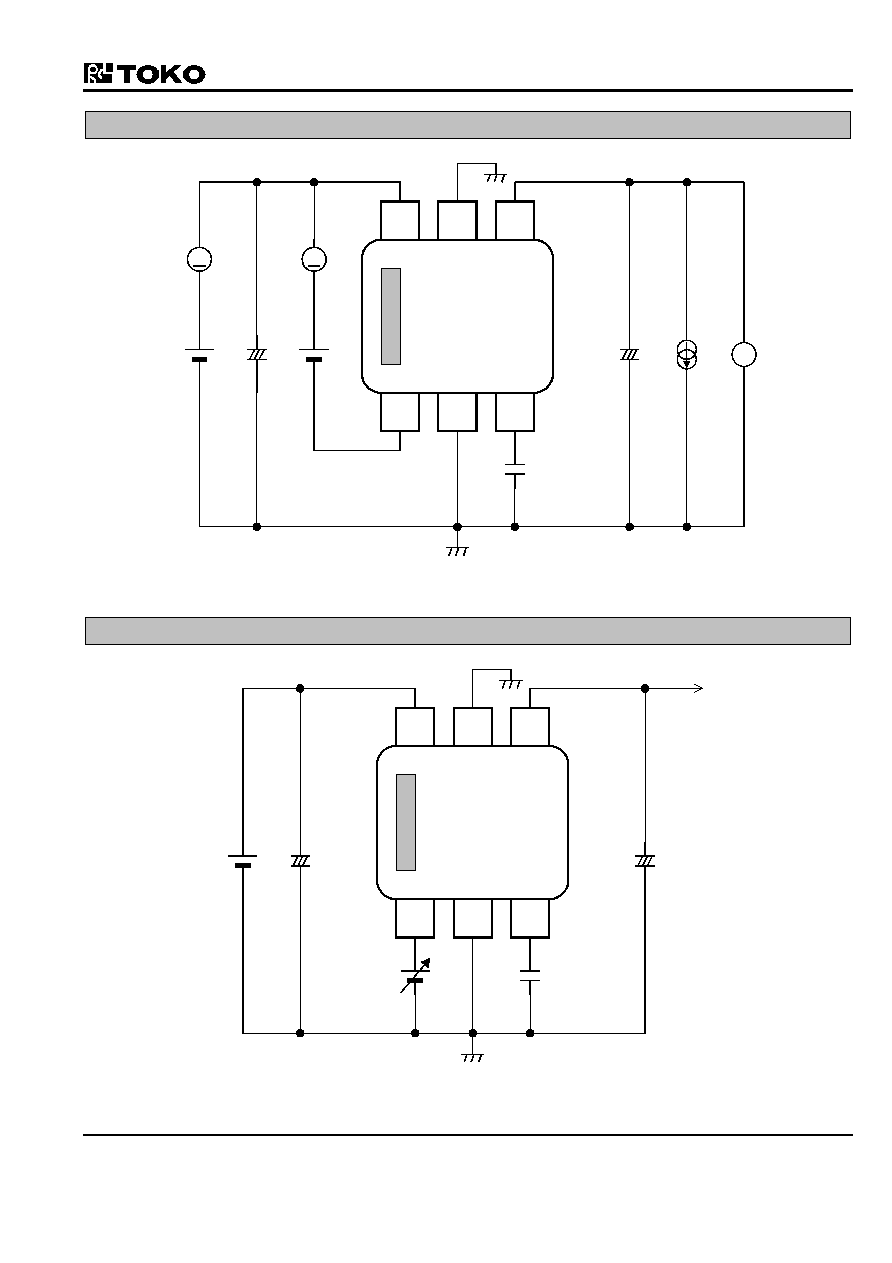
9. TEST CIRCUIT
Vin
Icont
V
Iin
Cin
Iout
Vout
1.0
�
F
1.0
�
F
0.1
�
F
V
A
+
1
3
2
6
4
Vin
Vout
Np
GND
Vcont
5
GND
CL
+
Cnp
*2pin,5pin are connected in the IC.
A
10. APPLICATION EXAMPLE
Vin
Cin
Vout
0.22
�
F
0.22
�
F
0.01
�
F
+
1
3
2
6
4
Vin
Vout
Np
GND
Vcont
5
GND
CL
+
Cnp
TK113xxCM
GC3-I013B
Page 9
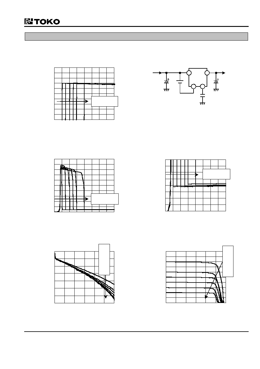
11. TYPICAL CHARACTERISTICS
11-1.DC CHARACTERISTICS
n
Line Regulation
-35
-30
-25
-20
-15
-10
-5
0
5
10
15
0
4
8
12
16
Vin (V)
Vout (mV)
113xx
Cnp
0.1
�
F
CL
1
�
F
Iout=5mA
Cin
1
�
F
Vcont
1.8V
Vin
=Vout
TYP
+1V
1
3
6
4
n
Vin vs Iin
n
Vin vs Iin
0
200
400
600
800
1000
1200
1400
1600
1800
2000
0
4
8
12
16
Vin (V)
Iin (
�
A)
0
20
40
60
80
100
120
140
160
0
4
8
12
16
Vin (V)
Iin (
�
A)
n
Load Regulation
n
Short Circuit Current
-60
-50
-40
-30
-20
-10
0
10
0
50
100
150
200
250 300
Iout (mA)
Vout (mV)
0
2
4
6
8
10
0
100
200 300
400
500 600
Iout (mA)
Vout (V)
Vout
=2, 3, 4, 5, 6, 8V
Vout
=2, 3, 4, 5, 6, 8V
Vout
=2, 3, 4, 5, 6, 8V
Vout
2V
3V
4V
5V
6V
8V
Vout
8V
6V
5V
4V
3V
2V

TK113xxCM
GC3-I013B
Page 10
n
Reverse Bias Current
0
20
40
60
80
0
2
4
6
8
10
12
Vrev(V)
Irev (
�
A)
113xx
Cnp
0.1
�
F
CL
1
�
F
Iout=5mA
Cin
1
�
F
Vcont
1.8V
Vin
=Vout
TYP
+1V
1
3
6
4
n
Dropout Voltage
n
Vin vs Vout Regulation Point
-240
-200
-160
-120
-80
-40
0
0
50
100 150 200 250
300
Iout(mA)
Vdrop(mV)
-140
-120
-100
-80
-60
-40
-20
0
20
40
60
-100
0
100
200
300
400
Vin
(mV) =Vin-VoutTYP
Vout
(mV)
n
Iin (Off state)
n
Vin-Vcont vs Icont
1.E-10
1.E-09
1.E-08
1.E-07
1.E-06
0
2
4
6
8
10 12 14 16
Vin (V)
Iin (A)
-1.0
-0.8
-0.6
-0.4
-0.2
0.0
0.0
0.5
1.0
1.5
2.0
Vcont(Reference : Vin) (V)
Icont (
�
A)
0
Vout=2V
Vout=3V
Vout=5V
Vout=4V
Vout=6V
Vout=8V
Iout=0, 50, 100, 150, 200, 300mA
Vout
TYP
Vout
Vout
Icont
-0.5
-1.0
-1.5
-2.0
TK113xxCM
GC3-I013B
Page 11
n
GND Pin Current
0
2
4
6
8
10
12
0
50
100
150
200
250 300
Iout (mA)
Ignd (mA)
113xx
Cnp
0.1
�
F
CL
1
�
F
Iout=5mA
Cin
1
�
F
Vcont
1.8V
Vin
=Vout
TYP
+1V
1
3
6
4
Temperature Characteristics
n
Iout MAX
n
GND Pin Current
300
350
400
450
500
550
-50
-25
0
25
50
75
100
Ta (
�
C)
IoutMax (mA)
0.0
2.0
4.0
6.0
8.0
10.0
12.0
14.0
16.0
18.0
20.0
-50
-25
0
25
50
75
100
Ta (
�
C)
Ignd (mA)
n
Control Current
n
ON/OFF Point
-5
-4
-3
-2
-1
0
-50
-25
0
25
50
75
100
Ta (
�
C)
Icont (
�
A)
0.6
0.8
1.0
1.2
1.4
1.6
1.8
-50
-25
0
25
50
75
100
Ta (
�
C)
Vcont(Reference : Vin) (-V)
Vout_ON
Vout_OFF
Iout=300mA
200mA
100mA
50mA
Vin-Vcont = 4V
Vin-Vcont = 3V
Vin-Vcont = 2V
Vin-Vcont = 1.8V
TK113xxCM
GC3-I013B
Page 12
n
Dropout Voltage
0
50
100
150
200
250
300
350
400
-50
-25
0
25
50
75
100
Ta (
�
C)
Vdrop (mV)
113xx
Cnp
0.1
�
F
CL
1
�
F
Iout=5mA
Cin
1
�
F
Vcont
1.8V
Vin
=Vout
TYP
+1V
1
3
6
4
n
Vout (TK11320CM)
n
Vout (TK11330CM)
-100
-80
-60
-40
-20
0
20
40
60
80
100
-50
-25
0
25
50
75
100
Ta (
�
C)
Vout (mV)
-100
-80
-60
-40
-20
0
20
40
60
80
100
-50
-25
0
25
50
75
100
Ta (
�
C)
Vout (mV)
n
Vout (TK11340CM)
n
Vout (TK11350CM)
-100
-80
-60
-40
-20
0
20
40
60
80
100
-50
-25
0
25
50
75
100
Ta (
�
C)
Vout (mV)
-100
-80
-60
-40
-20
0
20
40
60
80
100
-50
-25
0
25
50
75
100
Ta (
�
C)
Vout (mV)
Iout=300mA
200mA
100mA
50mA

TK113xxCM
GC3-I013B
Page 13
n
Vout (TK11360CM)
-100
-80
-60
-40
-20
0
20
40
60
80
100
-50
-25
0
25
50
75
100
Ta (
�
C)
Vout (mV)
113xx
Cnp
0.1
�
F
CL
1
�
F
Iout=5mA
Cin
1
�
F
Vcont
1.8V
Vin
=Vout
TYP
+1V
1
3
6
4
n
Vout (TK11380CM)
-100
-80
-60
-40
-20
0
20
40
60
80
100
-50
-25
0
25
50
75
100
Ta (
�
C)
Vout (mV)
TK113xxCM
GC3-I013B
Page 14
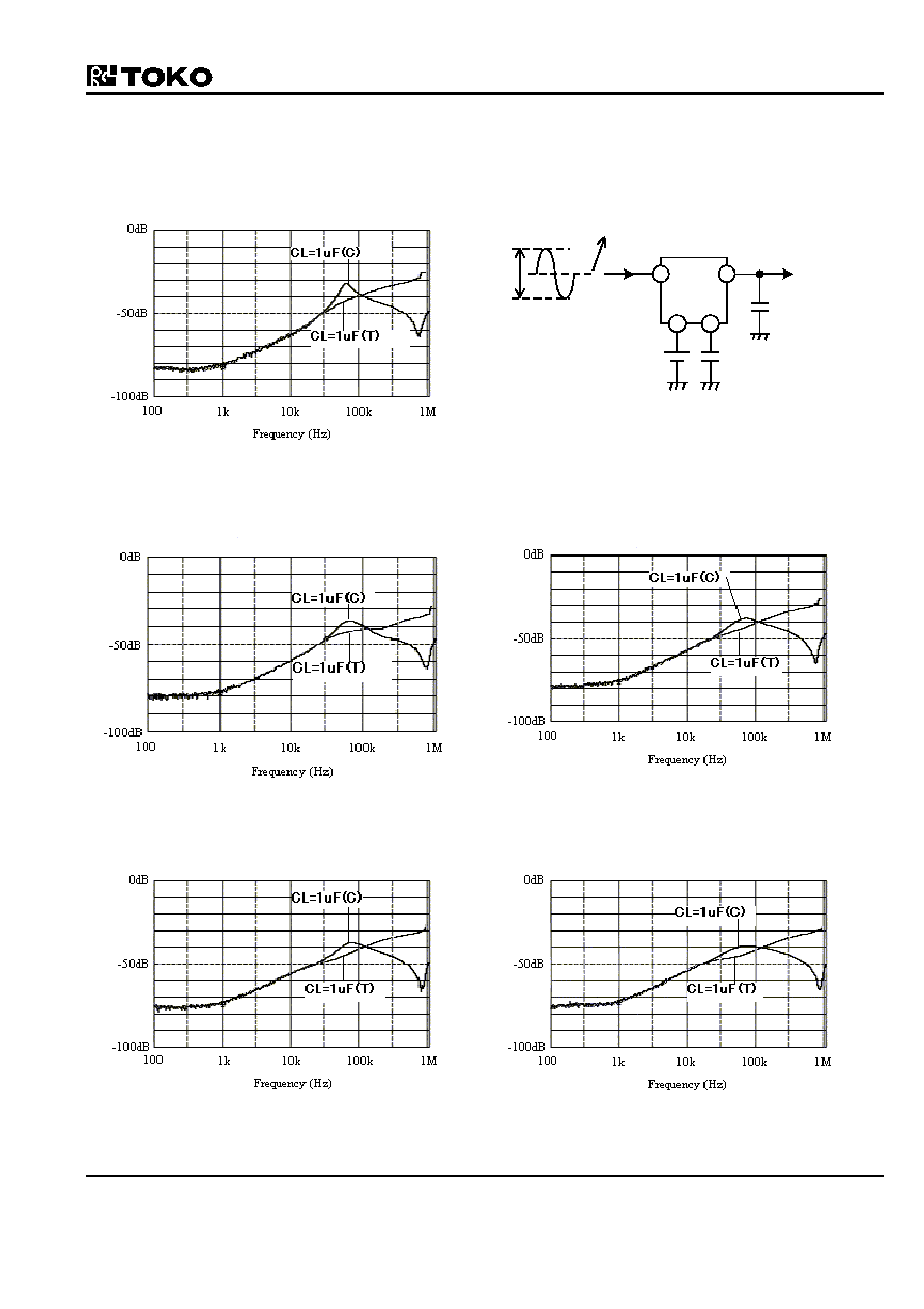
11-2. AC CHARACTERISTICS
Ripple Rejection
n
CL = 1
�
F : Ceramic (C) , Tantalum (T)
Vout=2V
113xx
Cnp
0.1
�
F
CL
1
�
F
Iout=10mA
Vcont
Vin-1.8V
1
3
6
4
Vin=Vout
TYP
+2V
f=100Hz
1MHz
500mVp-p
Vripple
n
CL = 1
�
F : Ceramic (C) , Tantalum (T)
Vout=3V
n
CL = 1
�
F : Ceramic (C) , Tantalum (T)
Vout=4V
n
CL = 1
�
F : Ceramic (C) , Tantalum (T)
Vout=5V
n
CL = 1
�
F : Ceramic (C) , Tantalum (T)
Vout=6V

TK113xxCM
GC3-I013B
Page 15
n
CL = 1
�
F : Ceramic (C) , Tantalum (T)
Vout=8V
113xx
Cnp
0.1
�
F
CL
1
�
F
Iout=10mA
Vcont
Vin-1.8V
1
3
6
4
Vin=Vout
TYP
+2V
f=100Hz
1MHz
500mVp-p
Vripple
n
CL = 0.22
�
F : Ceramic (C) , Tantalum (T)
Vout=3V
n
CL = 0.22
�
F, 10
�
F : Tantalum (T)
Vout=3V
n
Cnp = 0.001
�
F, 0.1
�
F : Tantalum (T)
Vout=3V
n
Iout=0.5
300mA
Vout=3V
-100
-90
-80
-70
-60
-50
-40
-30
-20
-10
0
0
50
100
150
200
250
300
Iout (mA)
R.R (dB)
Cnp=0.01� F
CL=0.22� F (C)
Freq=1kHz
Freq=400Hz
TK113xxCM
GC3-I013B
Page 16
n
Low Vin
Vout=3V
-100
-90
-80
-70
-60
-50
-40
-30
-20
-10
0
0.0 0.1 0.2 0.3 0.4 0.5 0.6 0.7 0.8 0.9 1.0
Vin-Vout_Typ (V)
R.R (dB)
113xx
Cnp
0.1
�
F
CL
1
�
F
Iout=10mA
Vcont
Vin-1.8V
1
3
6
4
Vin=Vout
TYP
+2V
f=100Hz
1MHz
500mVp-p
Vripple
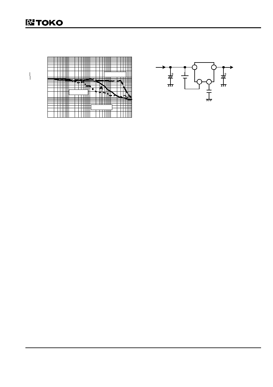
The ripple rejection (R.R) characteristic depends on the
characteristic and the capacitance value of the capacitor
connected to the output side. The R.R characteristic of
50kHz or more varies greatly with the capacitor on the
output side and PCB pattern. If necessary, please confirm
stability while operating.
Freq=1kHz, Cnp=0.01
�
F
CL=0.22
�
F (C), Vripple=100mVp-p
Iout=300mA
250mA
200mA
150mA
100mA
50mA
1mA

TK113xxCM
GC3-I013B
Page 17
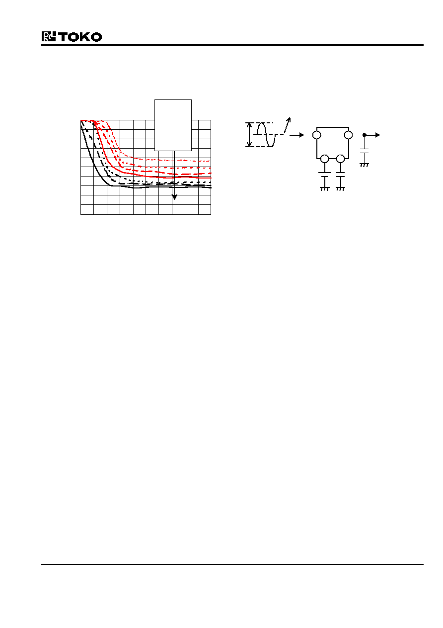
ON/OFF Transient
113xx
Cnp
CL
Iout=30mA
Cin
1
�
F
Vcont
Vin
=Vout
TYP
+1V
1
3
6
4
Vin
(Vin-2V)
f=100Hz
n
CL=0.22
�
F, 1.0
�
F, 2.2
�
F
Vout=3V
n
CL=0.22
�
F, 1.0
�
F, 2.2
�
F
Vout=3V
n
Cnp=0.001
�
F, 0.01
�
F, 0.1
�
F
Vout=3V
n
Cnp=0.001
�
F, CL=0.22
�
F, 1.0
�
F, 2.2
�
F
Vout=3V
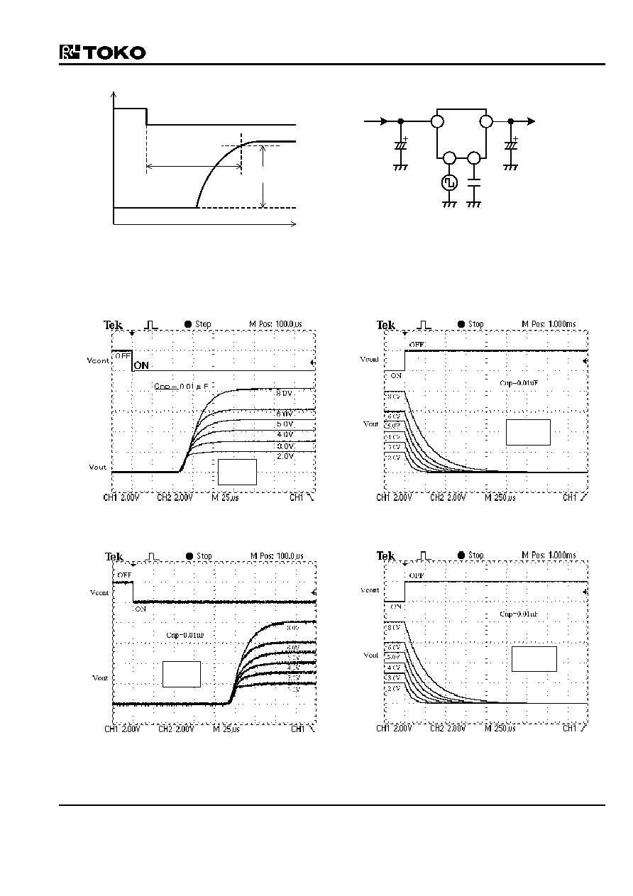
The rise time of the regulator depends on CL and Cnp; the
fall time depends on CL.
1V/div
50
�
s/div
1V/div
250
�
s/div
1V/div
10
�
s/div
1V/div
250
�
s/div
TK113xxCM
GC3-I013B
Page 18
Rise Time
Vout�95%
Vcont
Vout
Time
Voltage
113xx
Cnp
CL
Iout=30mA
Cin
1
�
F
Vcont
Vin
=Vout
TYP
+1V
1
3
6
4
Vin
(Vin-2V)
f=100Hz
n
Vout=2V, 3V, 4V, 5V, 6V, 8V
n
Vout=2V, 3V, 4V, 5V, 6V, 8V
n
Vout=2V, 3V, 4V, 5V, 6V, 8V
Vcont : one pulse (after discharge Cnp, CL)
n
Vout=2V, 3V, 4V, 5V, 6V, 8V
Vcont : one pulse (after discharge Cnp, CL)
2V/div
25
�
s/div
2V/div
250
�
s/div
2V/div
25
�
s/div
2V/div
250
�
s/div
TK113xxCM
GC3-I013B
Page 19
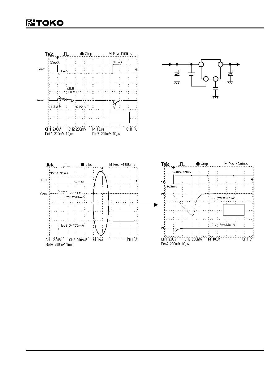
LOAD Transient
n
CL=0.22
�
F, 1.0
�
F, 2.2
�
F, Iout=3
33mA
11330
Cnp
0.01
�
F
CL
Cin
1
�
F
Vcont
1.8V
Vin
=Vout
TYP
+1V
1
3
6
4
Iout
ON
OFF
n
Iout=0
30mA, 3
33mA
n
Iout=0
30mA, 3
33mA
The output load transient characteristics can be greatly
improved by adding a small load current to ground. (Refer
to the above data curve)
Increase the output capacitance CL when the load current
change is fast and/or large.
200mV/div
10
�
s/div
200mV/div
1ms/div
200mV/div
10
�
s/div

TK113xxCM
GC3-I013B
Page 20
LINE Transient
n
CL=0.22
�
F, 1.0
�
F, 2.2
�
F
11330
Cnp
0.01
�
F
CL
1
�
F
Iout=30mA
Vcont
Vin-1.8V
1
3
6
4
Vin
4V
5V
n
Cnp=0.001
�
F, 0.01
�
F, 0.1
�
F
10mV/div
100
�
s/div
10mV/div
100
�
s/div
TK113xxCM
GC3-I013B
Page 21
Output Noise Characteristics
n
Vout vs Noise
10
20
30
40
50
60
70
80
90
100
2.0
3.0
4.0
5.0
6.0
7.0
8.0
Vout(V)
Noise (
�
Vrms)
CL=1.0� F (Tantal)
113xx
Cnp
0.01
�
F
CL
1
�
F
Iout=30mA
Cin
1
�
F
Vcont
1.8V
Vin
=Vout
TYP
+1V
1
3
6
4
BPF=400Hz
80kHz
n
Cnp vs Noise (CL : Tantalum)
Vout=3.0V
n
Cnp vs Noise (CL : Ceramic)
Vout=3.0V
0
50
100
150
200
250
300
1
10
100
1000
10000
100000
Cnp (pF)
Noise
�
Vrms)
CL=0.22uF
CL=0.47uF
CL=1.0uF
CL=2.2uF
CL=10uF
0
50
100
150
200
250
300
1
10
100
1000
10000
100000
Cnp (pF)
Noise
�
Vrms)
CL=0.22uF
CL=0.47uF
CL=1.0uF
CL=2.2uF
CL=10uF
n
Iout vs Noise (CL : Tantal)
Vout=3.0V
n
Iout vs Noise (CL : Ceramic)
Vout=3.0V
30
35
40
45
50
55
60
65
70
0
50
100
150
200
250
300
Iout (mA)
Noise (
�
Vrms)
CL=0.22uF
CL=0.47uF
CL=1.0uF
CL=2.2uF
CL=10uF
30
35
40
45
50
55
60
65
70
0
50
100
150
200
250
300
Iout (mA)
Noise (
�
Vrms)
CL=0.22uF
CL=0.47uF
CL=1.0uF
CL=2.2uF
CL=10uF
TK113xxCM
GC3-I013B
Page 22
n
Frequency vs Noise
CL=0.22
�
F(Ceramic), Iout=10mA, Vout=3V
0.01
0.1
1
10
10
100
1000
10000
100000
Frequency (Hz)
Noise (
�
V/
Hz )
113xx
Cnp
0.01
�
F
CL
1
�
F
Iout=30mA
Cin
1
�
F
Vcont
1.8V
Vin
=Vout
TYP
+1V
1
3
6
4
BPF=400Hz
80kHz
For better noise reduction, it is more effective to increase
noise bypass capacitance Cnp without increasing output
capacitance CL. The amount of noise increases with
higher output voltages.
Cnp=0.1
�
F
Cnp=1000pF
1k
10k
100k
Cnp=0.01
�
F

TK113xxCM
GC3-I013B
Page 23
12. PIN DESCRIPTION
Pin No. Pin Description
Internal Equivalent Circuit
Description
1
Vcont
1
Vin
Vcont
100k
On/Off Control Terminal
Vcont < Vin-1.8V : ON
Vcont > Vin-0.6V : OFF
*C Rank
The pull-up resister is not built-in.
2
GND
GND Terminal
3
Np
Np
3
Noise Bypass Terminal
Connect a bypass capacitor between GND.
4
Vout
Vout
Vin
Vref
4
Output Terminal
5
GND
GND Terminal
6
Vin
Input Terminal

TK113xxCM
GC3-I013B
Page 24
13. APPLICATIONS INFORMATION
13-1. Stability
Linear regulators require input and output capacitors in
order to maintain the regulator's loop stability. If a 0.1
�
F
capacitor is connected to the output side, the IC provides
stable operation at any voltage in the practical current
region. However, increase the CL capacitance when
using the IC in the low current region and low voltage.
Otherwise, the IC oscillates.
The equivalent series resistance (ESR) of the output
capacitor must be in the stable operation area. However,
it is recommended to use as large a value of capacitance
as is practical. The output noise and the ripple noise
decrease as the capacitance value increases. ESR values
vary widely between ceramic and tantalum capacitors.
However, tantalum capacitors are assumed to provide
more ESR damping resistance, which provides greater
circuit stability. This implies that a higher level of circuit
stability can be obtained by using tantalum capacitors
when compared to ceramic capacitors with similar values.
A recommended value of the application is as follows.
Cin=CL
0.22
�
F at Iout
0.5mA
TK113xxCM
Cin
0.22
�
F
Vin
Vout
CL
0.22
�
F
Cnp
0.01
�
F
GND
However, above recommended value does not satisfy
some conditions.
See "Output Voltage, Output Current vs. Stable
Operation Area" on the next page.
Select the CL capacitance according to the condition of
use.
If the fast load transient response is necessary, increase
the CL capacitance as much as possible.
The input capacitor is necessary when the battery is
discharged, the power supply impedance increases, or the
line distance to the power supply is long.
This capacitor might be necessary on each individual IC
even if two or more regulator ICs are used. It is not
possible to determine this indiscriminately. Please
confirm the stability while mounted

TK113xxCM
GC3-I013B
Page 25
Output Voltage, Output Current vs. Stable Operation Area
Vout=6.0V
0.01
0.1
1
10
100
0
50
100
150
Iout [mA]
ESR [ohm]
Stable Area
CL=0.1uF
Unstable Area
Vout=5.0V
0.01
0.1
1
10
100
0
50
100
150
Iout [mA]
ESR [ohm]
Stable Area
CL=0.1uF
Unstable Area
Vout=3.0, 4.0V
0.01
0.1
1
10
100
0
50
100
150
Iout [mA]
ESR [ohm]
Stable Area
CL=0.1uF
Vout=2.0V
0.01
0.1
1
10
100
0
50
100
150
Iout [mA]
ESR [ohm]
Stable Area
CL=0.1uF
Vout=8.0V
0.01
0.1
1
10
100
0
50
100
150
Iout [mA]
ESR [ohm]
Stable Area
CL=0.1uF
Unstable Area
The above graphs show stable operation with a ceramic
capacitor of 0.1
�
F (excluding the low current region). If
the capacitance is not increased in the low voltage, low
current area, stable operation may not be achieved. Please
select the best output capacitor according to the voltage
and current used. The stability of the regulator improves if
a big output side capacitor is used (the stable operation
area extends.) Please use as large a capacitance as is
practical. Although operation above 150mA has not been
described, stability is equal to or better than operation at
150mA.
For evaluation
Kyocera : CM05B104K10AB , CM05B224K10AB ,
CM105B104K16A , CM105B224K16A ,
CM21B225K10A
Murata : GRM36B104K10 , GRM42B104K10 ,
GRM39B104K25 , GRM39B224K10 ,
GRM39B105K6.3
ex. Ceramic Capacitance vs Voltage, Temperature
Generally, a ceramic capacitor has both a temperature
characteristic and a voltage characteristic. Please consider
both characteristics when selecting the part. The B curves
are the recommend characteristics.
%
Capacitance vs. Voltage
0
Bias Voltage (V)
CAP
2
4
6
8
10
50
60
70
80
90
100
B Curve
F Curve
Capacitance vs. Temperature
%
60
50
80
90
100
70
CAP
-50
-25
0
25
50
75
100
Ta (
�
C)
B Curve
F Curve
0.5
0.5
0.5
0.5
0.5

TK113xxCM
GC3-I013B
Page 26
13-2. Definition of term
Output Voltage (Vout)
The output voltage is specified with Vin=(Vout
TYP
+1V)
and Iout=5mA.
Maximum Output Current (Iout MAX)
The rated output current is specified under the condition
where the output voltage drops 0.9V times the value
specified with Iout=5mA. The input voltage is set to
Vout
TYP
+1V and the current is pulsed to minimize
temperature effect.
Dropout Voltage (Vdrop)
The dropout voltage is the difference between the input
voltage and the output voltage at which point the regulator
starts to fall out of regulation. Below this value, the output
voltage will fall as the input voltage is reduced. It is
dependent upon the load current and the junction
temperature.
Line Regulation (LinReg)
Line regulation is the ability of the regulator to maintain a
constant output voltage as the input voltage changes. The
line regulation is specified as the input voltage is changed
from Vin=Vout
TYP
+1V to Vin=Vout
TYP
+6V. It is a pulse
measurement to minimize temperature effect.
Load Regulation (LoaReg)
Load regulation is the ability of the regulator to maintain a
constant output voltage as the load current changes. It is a
pulsed measurement to minimize temperature effects with
the input voltage set to Vin=Vout
TYP
+1V. The load
regulation is specified under an output current step
condition of 5mA to 100mA.
Ripple Rejection (R.R)
Ripple rejection is the ability of the regulator to attenuate
the ripple content of the input voltage at the output. It is
specified with 500mV
rms
, 1kHz super-imposed on the input
voltage, where Vin=Vout+2V. Ripple rejection is the ratio
of the ripple content of the output vs. input and is
expressed in dB.
Standby Current (Istandby)
Standby current is the current which flows into the
regulator when the output is turned off by the control
function (Vcont=Vin).
Over Current Sensor
The over current sensor protects the device when there is
excessive output current. It also protects the device if the
output is accidentally connected to ground. (When
external transistor is used, the protection operates at 10mA
at the base terminal)
Thermal Sensor
The thermal sensor protects the device in case the junction
temperature exceeds the safe value (T
J
=150
�
C). This
temperature rise can be caused by external heat, excessive
power dissipation caused by large input to output voltage
drops, or excessive output current. The regulator will shut
off when the temperature exceeds the safe value. As the
junction temperatures decrease, the regulator will begin to
operate again. Under sustained fault conditions, the
regulator output will oscillate as the device turns off then
resets. Damage may occur to the device under extreme
fault.
Please prevent the loss of the regulator when this
protection operates, by reducing the input voltage or
providing better heat efficiency.
* In the case that the power, Vin
�
Ishort(Short Circuit Current),
becomes more than twice of the maximum rating of its power
dissipation in a moment, there is a possibility that the IC is
destroyed before internal thermal protection works.
Reverse Voltage Protection
Reverse voltage protection prevents damage due to the
output voltage being higher than the input voltage. This
fault condition can occur when the output capacitor
remains charged and the input is reduced to zero, or when
an external voltage higher than the input voltage is applied
to the output side
ESD
MM : 200pF 0
200V or more
HBM : 100pF 1.5k
2000V or more
TK113xxCM
GC3-I013B
Page 27
13-3. Layout
on/off
Vin
Vout
PCB Material : Glass epoxy (t=0.8mm)
Please do derating with 4.8mW/
�
C at Pd=600mW and
25
�
C or more. Thermal resistance (
ja) is=208
�
C/W.
25
50
100
Pd(mW)
150
�
C
600
0
0
(85
�
C)
-4.8mW/
�
C
The package loss is limited at the temperature that the
internal temperature sensor works (about 150
�
C).
Therefore, the package loss is assumed to be an internal
limitation. There is no heat radiation characteristic of the
package unit assumed because of the small size. Heat is
carried away by the device being mounted on the PCB.
This value changes by the material and the copper pattern
etc. of the PCB. The losses are approximately 600mW.
Enduring these losses becomes possible in a lot of
applications operating at 25
�
C.
The overheating protection circuit operates when there are
a lot of losses with the regulator (When outside
temperature is high or heat radiation is bad). The output
current cannot be pulled enough and the output voltage
will drop when the protection circuit operates. When the
junction temperature reaches 150
�
C, the IC is shut down.
However, operation begins at once when the IC stops
operation and the temperature of the chip decreases.
How to determine the thermal resistance when
mounted on PCB
The thermal resistance when mounted is expressed as
follows:
Tj=
ja
�
Pd+Ta
Tj of IC is set around 150
�
C. Pd is the value when the
thermal sensor is activated.
If the ambient temperature is 25
�
C, then:
150=
ja
�
Pd+25
ja=125/Pd (
�
C /mW)
Pd is easily calculated.
Mount the IC on the print circuit board. Short between the
output pin and ground. after that, raise input voltage from
0V to evaluated voltage (see*1) gradually.
At shorted the output pin, the power dissipation P
D
can be
expressed as Pd=Vin
�
Iin.
The input current decreases gradually as the temperature
of the chip becomes high. After a while, it reaches the
thermal equilibrium. Use this currrent value at the thermal
equilibrium.
In almost all the cases, it shows 600mW(SOT23L-6) or
more.
*1 In the case that the power, Vin
�
Ishort(Short Circuit Current),
becomes more than twice of the maximum rating of its power
dissipation in a moment, there is a possibility that the IC is
destroyed before internal thermal protection works.
0
25
50
75
100
150
Pd(mW)
Pd
D Pd
2
3
5
4
Ta ()
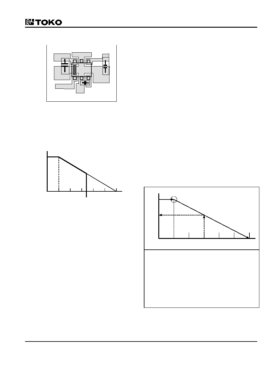
Procedure (When mounted on PCB.)
1. Find Pd (Vin
�
Iin when the output side is short-circuited).
2. Plot Pd against 25
�
C.
3. Connect Pd to the point corresponding to the 150
�
C with a
straight line.
4. In design, take a vertical line from the maximum operating
temperature (e.g., 75
�
C) to the derating curve.
5. Read off the value of Pd against the point at which the vertical
line intersects the derating curve. This is taken as the maximum
power dissipation DPd.
6. DPd
�
(Vinmax
-
Vout)=Iout (at 75
�
C)
The maximum output current at the highest operating
temperature will be Iout
DPd
�
(VinMax
-
Vout).
Please use the device at low temperature with better
radiation. The lower temperature provides better quality.
TK113xxCM
GC3-I013B
Page 28
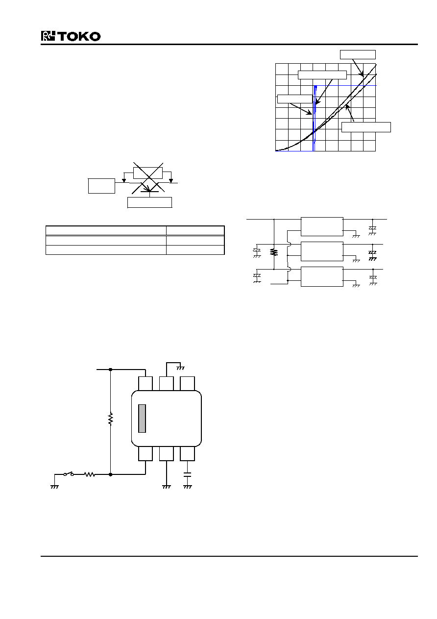
13-4. On/Off Control
It is recommended to turn the regulator Off when the
circuit following the regulator is non-operating. A design
with little electric power loss can be implemented. We
recommend the use of the on/off control of the regulator
without using a high side switch to provide an output from
the regulator. A highly accurate output voltage with low
voltage drop is obtained.
Because the control current is small, it is possible to
control it directly by CMOS logic.
REG
Vsat
On/Off Cont.
Control Terminal Voltage (Vcont)
ON/OFF State
Vcont < Vin-1.8V
ON
Vcont > Vin-0.6V
OFF
*C Rank
The pull-up resister is not built-in at control terminal. If a
pull-up resister is necessary according as the control driver,
connect the control terminal with a pull-up resistance (Rp-
up).
If the control function is not used, connect the control
terminal to GND.
It is possible to reduce the control current by inserting a
series resister (Rc). However, be careful the ON/OFF level
may change. Or "will change"
6
5
4
1
2
3
Vin
GND
GND
Vout
Vcont
Np
Vin
Rp-up
Rc
Cnp
SW
-0.8
-0.6
-0.4
-0.2
0.0
1.0
1.2
1.4
1.6
1.8
Vcont(Reference : Vin) (-V)
Icont (
�
A)
0
Parallel Connected ON/OFF Control
2.0V
5V
3.3V
On/Off Cont.
Vin
TK11350CM
R
TK11333CM
TK11320CM
Vout
The above figure is multiple regulators being controlled by
a single On/Off control signal. There is fear of overheating,
because the power loss of the low voltage side IC
(TK11320CM) is large. The series resistor (R) is put in the
input line of the low output voltage regulator in order to
prevent over-dissipation. The voltage dropped across the
resistor reduces the large input-to-output voltage across
the regulator, reducing the power dissipation in the device.
When the thermal sensor works, a decrease of the output
voltage, oscillation, etc. may be observed.
Vout
TYP
Vout
Vout (Rc=100k
)
Icont (Rc=100k
)
Vout (Rc=0)
Icont (Rc=0)

TK113xxCM
GC3-I013B
Page 29
13-5. Noise Bypass
The noise and the ripple rejection characteristics depend
on the capacitance on the Np terminal.
The ripple rejection characteristic of the low frequency
region improves by increasing the capacitance of Cnp.
A standard value is Cnp=0.1
�
F. Increase Cnp in a design
with important output noise and ripple rejection
requirements. The IC will not be damaged if the capacitor
value is increased.
The on/off switching speed changes depending on the Np
terminal capacitance. The switching speed slows when the
capacitance is large.

TK113xxCM
GC3-I013B
Page 30
13-6. Outline ; PCB ; Stamps
SOT23L-6
5-0.32
1.2
0.15
(0.3)
3.3
2.2
0.4
3.0
0.6
1.0
Reference Mount Pad
1
3
4
6
0~0.1
1.4max
�0.2
�0.3
�0.1
�0.2
0.4
0.1
0.10
+0.10
-
0.05
+0.10
-
0.05
0.95
+0.10
-
0.05
15�max
M
0.95
0.95
0.95
0.10
M
�0.2
3.4
Voltage
Code
Type
Code
X X R
Unit : mm
Package Structure
Package Material : Epoxy Resin
Terminal Material : Copper Alloy
Mass (Reference) : 0.023g
V OUT
V CODE
V OUT
V CODE
V OUT
V CODE
2.0V
20
3.2V
32
6.0V
60
2.1
21
3.3
33
8.0
80
2.2
22
3.5
35
2.5
25
3.8
38
2.6
26
4.0
40
2.7
27
4.5
45
2.8
28
4.7
47
2.9
29
4.8
48
3.0
30
5.0
50
3.1
31
5.5
55
The output voltage table indicates the standard value when manufactured.
Please contact your authorized Toko representative for voltage availability.

TK113xxCM
GC3-I013B
Page 31
14. NOTES
n
Please be sure that you carefully discuss your planned
purchase with our office if you intend to use the products in
this application manual under conditions where particularly
extreme standards of reliability are required, or if you intend
to use products for applications other than those listed in this
application manual.
l
Power drive products for automobile, ship or aircraft
transport systems; steering and navigation systems,
emergency signal communications systems, and any
system other than those mentioned above which include
electronic sensors, measuring, or display devices, and
which could cause major damage to life, limb or property
if misused or failure to function.
l
Medical devices for measuring blood pressure, pulse,
etc., treatment units such as coronary pacemakers and heat
treatment units, and devices such as artificial organs and
artificial limb systems which augment physiological
functions.
l
Electrical instruments, equipment or systems used in
disaster or crime prevention.
n
Semiconductors, by nature, may fail or malfunction in
spite of our devotion to improve product quality and
reliability. We urge you to take every possible precaution
against physical injuries, fire or other damages which may
cause failure of our semiconductor products by taking
appropriate measures, including a reasonable safety margin,
malfunction preventive practices and fire-proofing when
designing your products.
n
This application manual is effective from Oct. 2002. Note
that the contents are subject to change or discontinuation
without notice. When placing orders, please confirm
specifications and delivery condition in writing.
n
TOKO is not responsible for any problems nor for any
infringement of third party patents or any other intellectual
property rights that may arise from the use or method of use
of the products listed in this application manual. Moreover,
this application manual does not signify that TOKO agrees
implicitly or explicitly to license any patent rights or other
intellectual property rights which it holds.
n
None of ozone depleting substances(ODS) under the
Montreal Protocol is used in manufacturing process of us.
15. OFFICES
If you need more information on this product and other
TOKO products, please contact us.
n
TOKO Inc. Headquarters
1-17, Higashi-yukigaya 2-chome, Ohta-ku, Tokyo,
145-8585, Japan
TEL: +81.3.3727.1161
FAX: +81.3.3727.1176 or +81.3.3727.1169
Web site:
http://www.toko.co.jp/
n
TOKO America
Web site:
http://www.toko.com/
n
TOKO Europe
Web site:
http://www.tokoeurope.com/
n
TOKO Hong Kong
Web site:
http://www.toko.com.hk/
n
TOKO Taiwan
Web site:
http://www.tokohc.com.tw/
n
TOKO Singapore
Web site:
http://www.toko.com.sg/
n
TOKO Seoul
Web site:
http://www.toko.co.kr/
n
TOKO Manila
Web site:
http://www.toko.com.ph/
n
TOKO Brazil
Web site:
http://www.toko.com.br/
MEETING YOUR NEEDS
TO BUILD THE QUALITY RELIED BY COSTOMERS
YOUR DISTRIBUTOR