11-20-94
TK114xx
January, 1995 TOKO, Inc.
Page 1
FEATURES
s
Low Dropout Voltage
s
Electronic ON/OFF Switch
s
Very Low Standby Current (ON, No Load)
s
Internal Thermal Shutdown
s
Short Circuit Protection
s
Very Low (<100 nA) Current in OFF Mode
s
Customized Versions Are Available
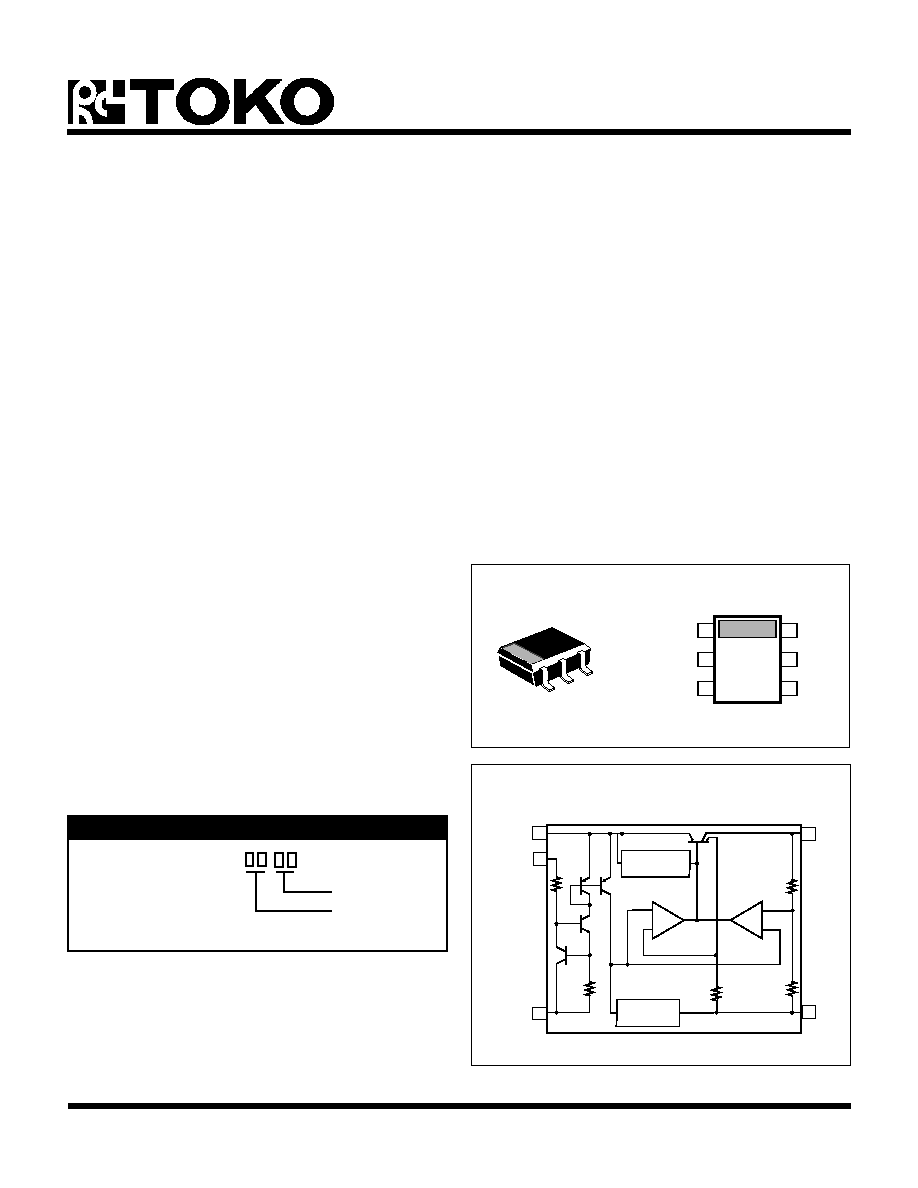
DESCRIPTION
The TK114xx is a low power, linear regulator with a built-
in electronic switch. The internal electronic switch can be
controlled by an external pull-up resistor and an open drain
or open collector transistor. The device is in the OFF state
when the control pin is biased from V
IN
through the pull-up
resistor.
An internal PNP pass-transistor is used in order to achieve
low dropout voltage (typically 200 mV at 50 mA load
current). The device has very low quiescent current (500
µ
A) in the ON mode with no load and 2 mA with 30 mA load.
The quiescent current is typically 4 mA at 60 mA load. An
internal thermal shutdown circuit limits the junction tem-
perature to below 150
∞
C. The load current is internally
monitored and the device will shut down (no load current)
in the presence of a short circuit at the output. The device
is available in a small SOT-23L surface mount package.
VOLTAGE REGULATOR WITH ON/OFF SWITCH
APPLICATIONS
s
Battery Powered Systems
s
Cellular Telephones
s
Pagers
s
Personal Communications Equipment
s
Portable Instrumentation
s
Portable Consumer Equipment
s
Radio Control Systems
s
Toys
s
Low Voltage Systems
BLOCK DIAGRAM
1
3
CONTROL
GND
6
4
V
IN
V
O
KT114xxM.PO
2
5
TK114xxM
TK114
Voltage Code
Tape/Reel Code
TAPE/REEL CODE
BX : Bulk/Bag
TL : Tape Left
ORDERING INFORMATION
VOLTAGE CODE
30 = 3.0 V
32 = 3.25 V
35 = 3.5 V
37 = 3.75 V
40 = 4.0 V
45 = 4.5 V
47 = 4.75 V
50 = 5.0 V
55 = 5.5 V
57 = 5.75 V
60 = 6.0 V
80 = 8.0 V
S
S
S
S
S
S
S
S
S
S
V
O
V
IN
LOW
CONTROL
(LC)
GND
KT114xx ∑ BD
TK114xx
BANDGAP
REFERENCE
≠
+
HIGH
CONTROL
(HC)
≠
+
S
S
S
S
THERMAL
PROTECTION
S
S
2
1
3
6
8
R3
TK114xx
11-20-94
Page 2
January, 1995 TOKO, Inc.
ABSOLUTE MAXIMUM RATINGS
Supply Voltage ......................................................... 16 V
Load Current ....................................................... 180 mA
Power Dissipation (Note 1) ................................ 400 mW
Storage Temperature Range ................... -55 to +150
∞
C
Operating Temperature Range .................. -30 to +80
∞
C
Lead Soldering Temp. (10 sec.) ........................... 240
∞
C
Junction Temperature .......................................... 150
∞
C
TK11430 ELECTRICAL CHARACTERISTICS
SYMBOL
PARAMETER
TEST CONDITION
MIN
TYP
MAX
UNITS
I
IN1
Supply Current 1
V
IN
= 4 V, I
O
= 0 mA
500
900
µ
A
I
IN2
Supply Current 2
V
IN
= 2.5 V, I
O
= 0 mA
1
2.5
µ
A
I
INS
Standby Current
V
IN
= 10 V, Output Off
0.1
µ
A
V
O
Output Voltage Regulation
V
IN
= 4 V, I
O
= 30 mA
2.9
3.0
3.1
%
V
DROP
Dropout Voltage
I
O
= 30 mA
0.12
0.3
V
I
O
Output Current
70
110
mA
I
OR
Recommended Output
70
mA
Current
LinReg
Line Regulation
V
IN
= 4 V
9 V
5
30
mV
LoaReg
Load Regulation
I
O
= 0 mA to 30 mA
18
50
mV
I
O
= 0 mA to 60 mA
36
80
mV
RR
Ripple Rejection
100 mV(rms), f = 400 Hz
55
dB
V
IN
= 4.5 V, I
O
= 10 mA
V/
T
V
O
Temperature Coefficient
V
IN
= 4.5 V, I
O
= 10 mA
±
0.3
mV/
∞
C
-20
∞
C
T
A
75
∞
C
V
N
Output Noise Voltage
V
IN
= 4.5 V, I
O
= 10 mA
180
µ
V(rms)
Control Pin
I
CONT
Control Pin Current
On Mode
35
120
µ
A
V
Coff
Control Pin Voltage
Off Mode
V
IN
-0.2
V
IN
V
V
Con
Control Pin Voltage
On Mode
0
0.6
V
Note 1: Power dissipation must be derated at the rate of 1.6 mW/
∞
C for operation above T
A
= 25
∞
C.
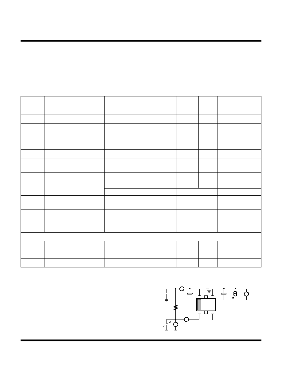
TEST CIRCUIT 1
KT114xx ∑ TC01A
1
4
5
6
2
3
S
V
IN
V
A
A
V
S
S
S
S
V
OUT
I
OUT
V
IN
V
OUT
1 F
m
10 F
m
150KW
I
CONT
CONT
CONT
GND
NOTE: CONNECT PINS 2 AND 5 TO
GND FOR MAXIMUM HEAT CONDUCTION.
+
+
+
_
+
_

11-20-94
TK114xx
January, 1995 TOKO, Inc.
Page 3
TK11432 ELECTRICAL CHARACTERISTICS
SYMBOL
PARAMETER
TEST CONDITION
MIN
TYP
MAX
UNITS
I
IN1
Supply Current 1
V
IN
= 4.2 V, I
O
= 0 mA
500
900
µ
A
I
IN2
Supply Current 2
V
IN
= 2.5 V, I
O
= 0 mA
1
2.5
µ
A
I
INS
Standby Current
V
IN
= 10 V, Output Off
0.1
µ
A
V
O
Output Voltage Regulation
V
IN
= 4.2 V, I
O
= 30 mA
3.13
3.25
3.37
%
V
DROP
Dropout Voltage
I
O
= 30 mA
0.12
0.3
V
I
O
Output Current
(Note 2)
70
110
mA
I
OR
Recommended Output
70
mA
Current
LinReg
Line Regulation
V
IN
= 4.2 V
9.2 V
6
30
mV
LoaReg
Load Regulation
V
IN
= 4.2 V, I
O
= 0 mA to 30 mA
20
50
mV
V
IN
= 4.2 V, I
O
= 0 mA to 60 mA
40
80
mV
RR
Ripple Rejection
100 mV(rms), f = 400 Hz
55
dB
V
IN
= 4.7 V, I
O
= 10 mA
V/
T
V
O
Temperature Coefficient
V
IN
= 4.7 V, I
O
= 10 mA
±
0.3
mV/
∞
C
-20
∞
C
T
A
75
∞
C
V
N
Output Noise Voltage
10 Hz
f
100 KHz, I
O
= 10 mA
180
µ
V(rms)
Control Pin
I
CONT
Control Pin Current
On Mode
35
120
µ
A
V
Coff
Control Pin Voltage
Off Mode
V
IN
-0.2
V
IN
V
V
Con
Control Pin Voltage
On Mode
0
0.6
V
Note 2: I
O
(Load Current) is current when V
O
drop down 0.3V from V
O
at I
O
= 30 mA.

TK114xx
11-20-94
Page 4
January, 1995 TOKO, Inc.
TK11435 ELECTRICAL CHARACTERISTICS
SYMBOL
PARAMETER
TEST CONDITION
MIN
TYP
MAX
UNITS
I
IN1
Supply Current 1
V
IN
= 4.5 V, I
O
= 0 mA
500
900
µ
A
I
IN2
Supply Current 2
V
IN
= 2.5 V, I
O
= 0 mA
1
2.5
µ
A
I
INS
Standby Current
V
IN
= 10 V, Output Off
0.1
µ
A
V
O
Output Voltage Regulation
V
IN
= 4.5 V, I
O
= 30 mA
3.38
3.5
3.62
%
V
DROP
Dropout Voltage
I
O
= 30 mA
0.12
0.3
V
I
O
Output Current
(Note 2)
70
110
mA
I
OR
Recommended Output
70
mA
Current
LinReg
Line Regulation
V
IN
= 4.5 V
9.5 V
7
35
mV
LoaReg
Load Regulation
I
O
= 0 mA to 30 mA
20
55
mV
I
O
= 0 mA to 60 mA
40
95
mV
RR
Ripple Rejection
100 mV(rms), f = 400 Hz
55
dB
V
IN
= 4.5 V, I
O
= 10 mA
V/
T
V
O
Temperature Coefficient
V
IN
= 4.5 V, I
O
= 10 mA
±
0.3
mV/
∞
C
-20
∞
C
T
A
75
∞
C
V
N
Output Noise Voltage
V
IN
= 4.5 V, I
O
= 10 mA
180
µ
V(rms)
Control Pin
I
CONT
Control Pin Current
On Mode
35
120
µ
A
V
Coff
Control Pin Voltage
Off Mode
V
IN
-0.2
V
IN
V
V
Con
Control Pin Voltage
On Mode
0
0.6
V
Note 2: I
O
(Load Current) is current when V
O
drop down 0.3V from V
O
at I
O
= 30 mA.
11-20-94
TK114xx
January, 1995 TOKO, Inc.
Page 5
TK11437 ELECTRICAL CHARACTERISTICS
SYMBOL
PARAMETER
TEST CONDITION
MIN
TYP
MAX
UNITS
I
IN1
Supply Current 1
V
IN
= 4.7 V, I
O
= 0 mA
500
900
µ
A
I
IN2
Supply Current 2
V
IN
= 2.7 V, I
O
= 0 mA
1
2.5
µ
A
I
INS
Standby Current
V
IN
= 10 V, Output Off
0.1
µ
A
V
O
Output Voltage Regulation
V
IN
= 4.7 V, I
O
= 30 mA
3.62
3.75
3.88
%
V
DROP
Dropout Voltage
I
O
= 30 mA
0.12
0.3
V
I
O
Output Current
(Note 2)
70
110
mA
I
OR
Recommended Output
70
mA
Current
LinReg
Line Regulation
V
IN
= 4.7 V
9.7 V
7
35
mV
LoaReg
Load Regulation
I
O
= 0 mA to 30 mA
20
110
mV
I
O
= 0 mA to 60 mA
40
100
mV
RR
Ripple Rejection
100 mV(rms), f = 400 Hz
55
dB
V
IN
= 5.2 V, I
O
= 10 mA
V/
T
V
O
Temperature Coefficient
V
IN
= 5.2 V, I
O
= 10 mA
±
0.4
mV/
∞
C
-20
∞
C
T
A
75
∞
C
V
N
Output Noise Voltage
V
IN
= 4.5 V, I
O
= 10 mA
180
µ
V(rms)
Control Pin
I
CONT
Control Pin Current
On Mode
35
120
µ
A
V
Coff
Control Pin Voltage
Off Mode
V
IN
-0.2
V
IN
V
V
Con
Control Pin Voltage
On Mode
0
0.6
V
Note 2: I
O
(Load Current) is current when V
O
drop down 0.3V from V
O
at I
O
= 30 mA.