 | –≠–ª–µ–∫—Ç—Ä–æ–Ω–Ω—ã–π –∫–æ–º–ø–æ–Ω–µ–Ω—Ç: TK65423M | –°–∫–∞—á–∞—Ç—å:  PDF PDF  ZIP ZIP |
September 1999 TOKO, Inc.
Page 1
TK654xx
ADVANCED INFORMATION
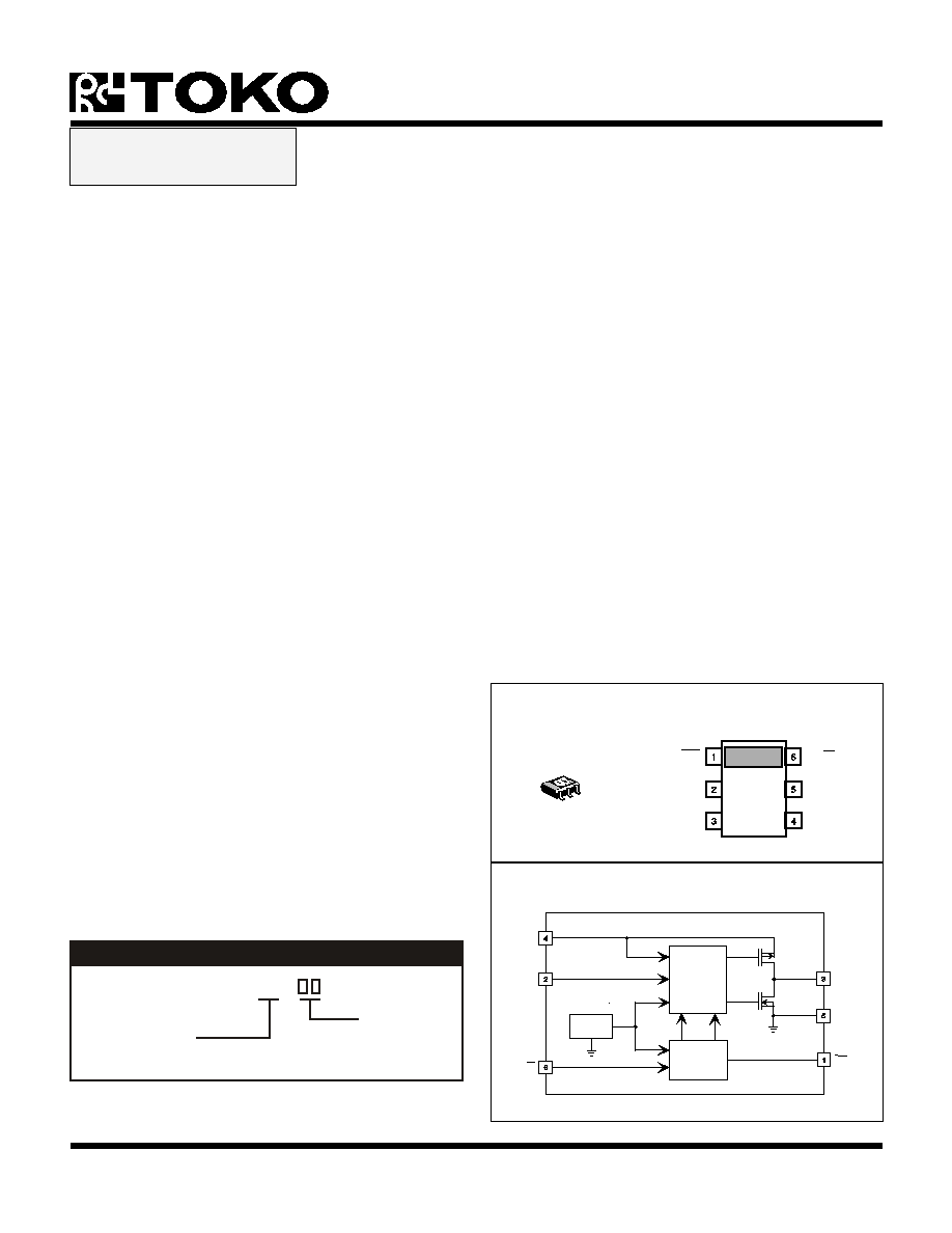
VOUT
VIN
LBO
LBI/SB
SW
CONTROL
CIRCUIT
BATTERY
MONITOR
REF
LBO
OFF
GND
FEATURES
s
Minimum External Component Count (1 coil, 1 cap)
s
Miniature 6 Pin SOT23L-6 Surface Mount Package
s
Up To 95% Efficient
s
Extremely Low Operating Current (24
µ
A)
s
Low Quiescent Current (18
µ
A)
s
Low Ripple
s
Fast Transient Response
s
Linear Dropout Characteristics
s
Short Circuit Protection
s
Regulates Down to 1.8 V
s
Synchronous Rectification
s
Internal Battery Monitor
BLOCK DIAGRAM
TK654xxM
VOUT
LBO
VIN
SW
GND
LBI/SB
ORDERING INFORMATION
TAPE/REEL CODE
TL: Tape Left
Tape/Reel Code
TK654xxM
Voltage Code
VOLTAGE CODE
18 = 1.8 V
21 = 2.1 V
24 = 2.4 V
25 = 2.5 V
27 = 2.7 V
30 = 3.0 V
33 = 3.3 V
ADVANCED
INFORMATION
APPLICATIONS
s
Battery Powered Systems
s
Cellular Telephones
s
Pagers
s
Personal Communications Equipment
s
Radio Controlled Systems
s
Toys
STEP-DOWN CONVERTER WITH BATTERY MONITOR
DESCRIPTION
The TK654xx low power step-down converter is designed
for portable battery systems, capable of operating from a
single Li-ion battery cell or multiple alkaline or rechargeable
(NiCd or NiMH) battery cells (up to 6 V). The TK654xx
provides the power switch, synchronous rectifier, and the
control circuit for a buck step-down converter. Only two
external components are required to complete the step-
down conversion.
The TK654xx provides laser-trimmed output voltages
ranging from 1.8 V to 3.3 V. The low resistance MOSFET
switch and synchronous rectifier allow average currents
up to 200 mA, while maintaining peak efficiencies up to
95%. A low-battery threshold and turn-off threshold can
be individually programmed by the user, utilizing a single
resistor divider connected to the Low Battery Input (LBI)
pin. When the resistively-divided supply voltage on the
LBI pin drops below approximately 1.22 V, the Low Battery
Output (LBO) pin will become asserted. The dual-function
LBI pin can alternatively be used as a Standby (SB) pin.
Driving the SB pin low will disable the TK654xx and drop
the quiescent current on the input supply to approximately
18
µ
A.
Pulse Current Amplitude control is used to regulate the
voltage at the V
OUT
pin of the IC. When the output voltage
of the TK654xx drops below the regulation threshold, a
current pulse is transferred from the input supply to the
output. The TK654xx utilizes a proprietary control scheme,
where the average amplitude of the current pulse is varied
depending upon the current loads. The proprietary
architecture allows fast transient response and minimal
ripple while maintaining ease-of-use and low component
count.
The TK654xx is available in a miniature 6-pin SOT23L-6
surface mount package.
Page 2
TK654xx
September 1999 TOKO, Inc.
ADVANCED INFORMATION
ABSOLUTE MAXIMUM RATINGS
All Pins Except GND ............................................... 6.5 V
Power Dissipation (Note 1) ................................ 400 mW
Storage Temperature Range ................... -55 to +150
∞
C
Operating Temperature Range ................... -20 to +80
∞
C
Junction Temperature ........................................... 150
∞
C
Lead Soldering Temperature (10 s.) ..................... 235
∞
C
TK654xx ELECTRICAL CHARACTERISTICS
Test conditions: V
IN
= 5 V, I
OUT
= 1 mA, T
A
= T
J
= Full Operating Temperature Range, unless otherwise specified.
Note 1: Power dissipation is 400 mW when mounted as recommended. Derate at 3.2 mW/
∞
C for operation above 25
∞
C. Power dissipation is 200
mW in Free Air. Derate at 1.6 mW/
∞
C for operation above 25
∞
C
Note 2: V
REG
= 3.3, 3.0, 2.7, 2.5, 2.4, 2.1, 1.8 V.
Note 3: When using test circuit.
Note 4: When using test circuit and ramping V
IN
down.
Note 5: When using test circuit with SB pin resistors removed and tied to V
IN
. (V
IN
= 1.8 V)
Note 6: When using test circuit with SB pin resistors removed and tied to V
IN
. (V
IN
= 3.3 V)
P
L
O
B
M
Y
S
R
E
T
E
M
A
R
A
P
S
N
O
I
T
I
D
N
O
C
T
S
E
T
N
I
M
P
Y
T
X
A
M
S
T
I
N
U
V
N
I
e
g
a
t
l
o
V
t
u
p
n
I
2
6
V
V
)
G
E
R
(
T
U
O
e
g
a
t
l
o
V
t
u
p
t
u
O
T
A
T
=
J
)
2
e
t
o
N
(
C
∞
5
2
=
%
3
-
V
G
E
R
%
3
V
%
5
-
%
5
+
V
V
)
D
A
O
L
(
T
U
O
n
o
i
t
a
l
u
g
e
R
d
a
o
L
I
D
A
O
L
)
3
e
t
o
N
(
,
A
m
0
0
1
o
t
0
=
5
4
0
2
1
V
m
V
)
E
N
I
L
(
T
U
O
n
o
i
t
a
l
u
g
e
R
e
n
i
L
V
N
I
)
3
e
t
o
N
(
,
V
6
o
t
4
=
6
0
2
V
m
I
)
T
U
O
V
(
Q
V
o
t
n
i
t
n
e
r
r
u
C
t
n
e
c
s
e
i
u
Q
T
U
O
n
i
P
V
T
U
O
V
=
)
G
E
R
(
T
U
O
V
m
0
5
+
)
3
e
t
o
N
(
0
1
0
5
A
µ
I
)
N
I
V
(
Q
V
o
t
n
i
t
n
e
r
r
u
C
t
n
e
c
s
e
i
u
Q
N
I
n
i
P
V
T
U
O
V
=
)
G
E
R
(
T
U
O
V
m
0
5
+
5
1
5
6
A
µ
V
)
I
B
L
(
H
T
d
l
o
h
s
e
r
h
T
t
u
p
n
I
I
B
L
T
A
T
=
J
C
∞
5
2
=
7
5
1
.
1
2
2
.
1
2
8
2
.
1
V
V
)
B
S
(
H
T
d
l
o
h
s
e
r
h
T
y
b
d
n
a
t
S
T
A
T
=
J
C
∞
5
2
=
7
5
1
.
1
2
2
.
1
2
8
2
.
1
V
I
)
B
S
(
B
t
n
e
r
r
u
C
s
a
i
B
t
u
p
n
I
B
S
3
e
t
o
N
0
A
n
V
(
t
a
4
e
t
o
N
)
B
S
(
H
T
)
V
m
0
0
1
-
0
0
4
0
2
7
0
0
0
1
A
n
I
)
X
A
M
(
T
U
O
t
n
e
r
r
u
C
t
u
p
t
u
O
m
u
m
i
x
a
M
)
3
e
t
o
N
(
0
0
1
A
m
I
)
C
S
(
T
U
O
t
n
e
r
r
u
C
t
i
u
c
r
i
C
t
r
o
h
S
)
3
e
t
o
N
(
0
5
2
A
m
I
)
V
N
O
C
(
Q
t
n
e
r
r
u
C
t
n
e
c
s
e
i
u
Q
r
e
t
r
e
v
n
o
C
I
)
3
e
t
o
N
(
T
U
O
A
m
0
=
4
2
0
9
A
µ
I
Y
B
T
S
t
n
e
r
r
u
C
y
b
d
n
a
t
S
r
e
t
r
e
v
n
o
C
n
e
p
o
1
n
i
P
,
V
0
=
n
i
p
B
S
8
1
5
6
A
µ
F
F
E
y
c
n
e
i
c
i
f
f
E
r
e
t
r
e
v
n
o
C
I
T
U
O
)
3
e
t
o
N
(
,
A
m
0
5
=
T
A
T
=
J
)
8
1
4
5
6
K
T
(
C
∞
5
2
=
6
8
1
9
%
I
T
U
O
)
3
e
t
o
N
(
,
A
m
0
5
=
T
A
T
=
J
)
3
3
4
5
6
K
T
(
C
∞
5
2
=
0
9
5
9
%
V
P
O
R
D
e
g
a
t
l
o
V
t
u
o
p
o
r
D
I
T
U
O
)
5
e
t
o
N
(
,
A
m
0
5
=
T
A
T
=
J
)
8
1
4
5
6
K
T
(
C
∞
5
2
=
0
0
1
5
9
1
V
m
I
T
U
O
)
6
e
t
o
N
(
,
A
m
0
5
=
T
A
T
=
J
)
3
3
4
5
6
K
T
(
C
∞
5
2
=
5
7
5
4
1
V
m
September 1999 TOKO, Inc.
Page 3
TK654xx
ADVANCED INFORMATION
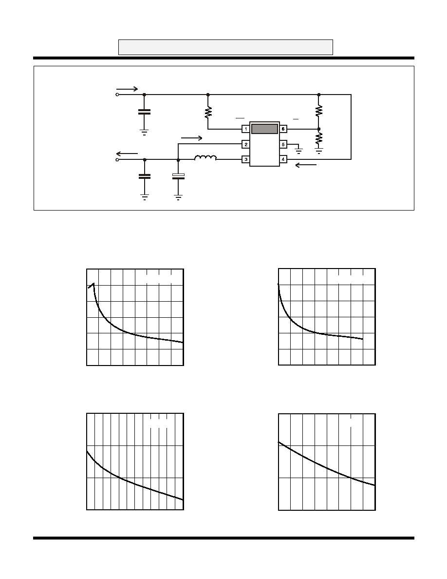
C1
10 µF
C2
10 µF
L1
100 µH
C3
10 µF
R3
300 K
VOUT
VIN = 5 V
R1
634 K
R2
287 K
LBI/SB
GND
VIN
LBO
VOUT
SW
+
IQ(CONV)
IQ(VOUT)
IOUT
IQ(VIN)
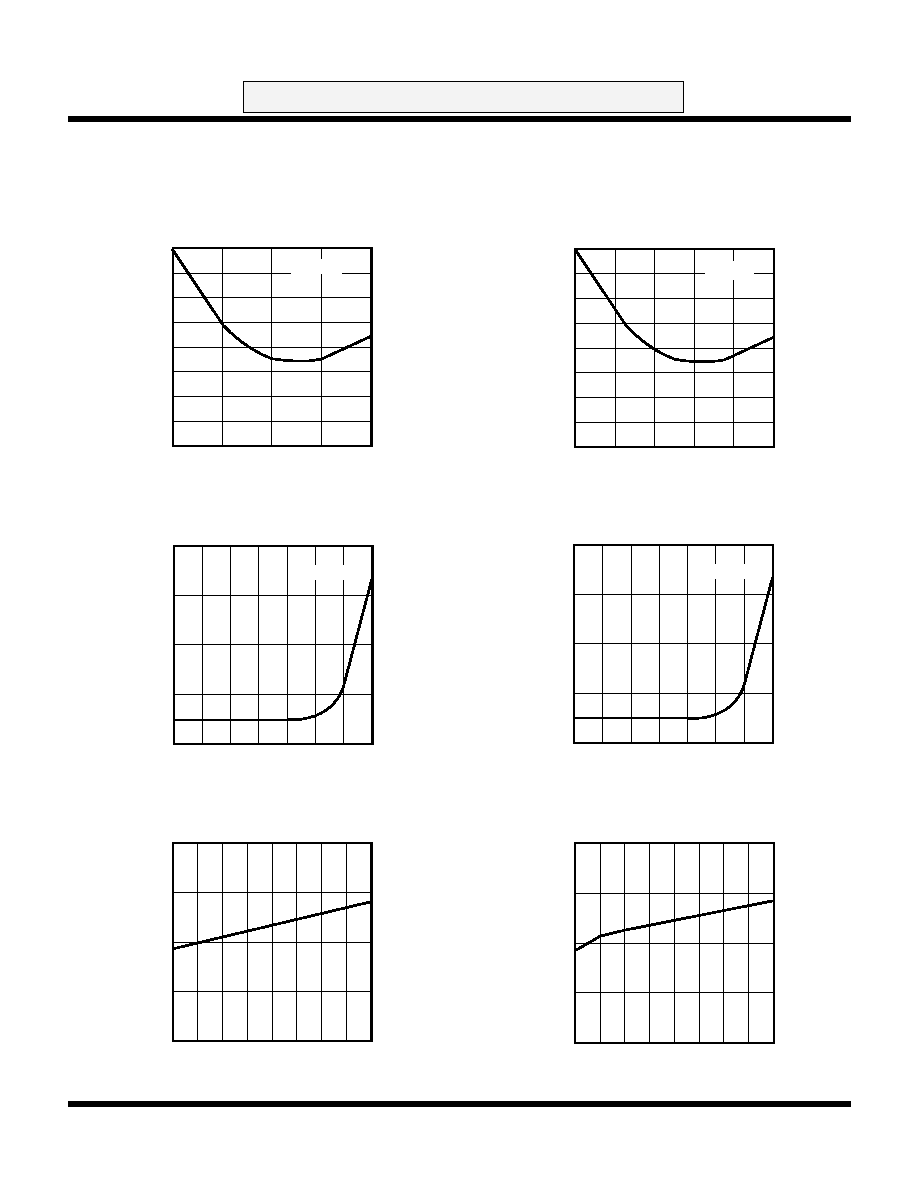
TYPICAL PERFORMANCE CHARACTERISTICS
USING TEST CIRCUIT
TEST CIRCUIT
L1:
L
1
: Toko D10F Coil, PN A814AY-101K
C
1
,C
3
: Ceramic 10
µ
F
C
2
: Tantalum 10
µ
F
V
OUT
(V)
1.810
TK65418
LINE REGULATION
VIN (V)
2.0 2.5 3.0 3.5 4.0 4.5 5.0 5.5 6.0
1.795
1.790
1.800
1.805
1.815
1.820
IOUT = 1 mA
V
OUT
(V)
TK65433
LINE REGULATION
VIN (V)
3.4 3.8 4.2 4.6 5.0 5.4 5.8 6.0
3.300
3.315
3.330
3.305
3.310
3.320
3.325
IOUT = 1 mA
V
OUT
(V)
TK65418
LOAD REGULATION
IOUT (mA)
0 20 40 60 80 100 120
1.76
1.78
1.80
1.82
VIN = 5 V
V
OUT
(V)
TK65433
LOAD REGULATION
IOUT (mA)
0 20 40 60 80 100 120 140 160
3.2
3.25
3.3
3.35
VIN = 5 V
Page 4
TK654xx
September 1999 TOKO, Inc.
ADVANCED INFORMATION
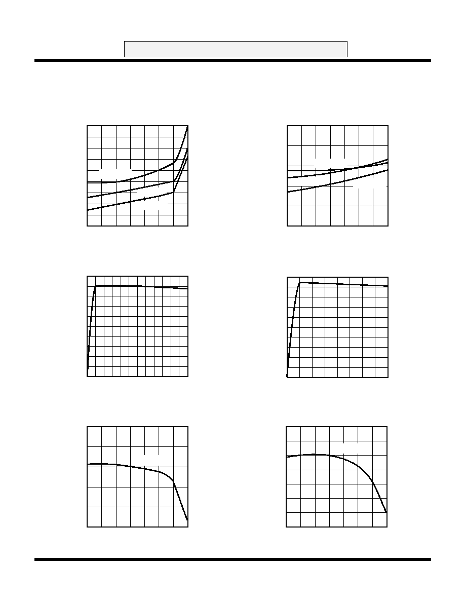
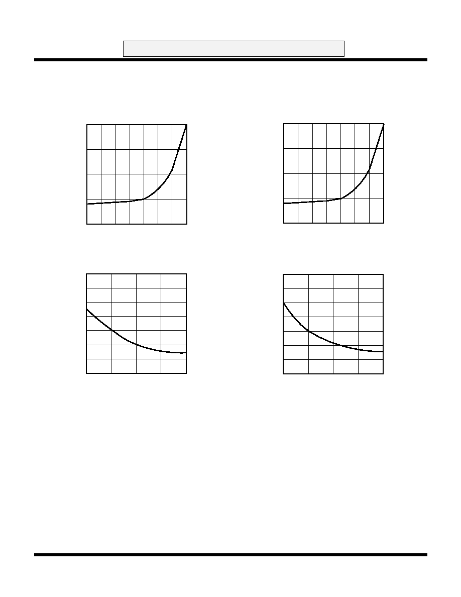
TYPICAL PERFORMANCE CHARACTERISTICS
USING TEST CIRCUIT (CONT.)
V
OUT
(V)
1.8
TK65418
LOAD AND TEMPERATURE
REGULATION
TEMPERATURE (
∞
C)
-50 -25 0 25 50 75 100 125
1.72
1.76
1.84
1.90
1.74
1.82
1.88
1.78
1.86
I
OUT
= 1 mA
I
OUT
= 50 mA
I
OUT
= 100 mA
V
OUT
(V)
3.35
TK65433
LOAD AND TEMPERATURE
REGULATION
TEMPERATURE (
∞
C)
-50 -25 0 25 50 75 100 125
3.05
3.45
3.55
3.15
3.25
I
OUT
= 1 mA
I
OUT
= 50 mA
I
OUT
= 100 mA
EFFICIENCY (%)
40
TK65418
EFFICIENCY vs.
OUTPUT CURRENT
IOUT (mA)
0 20 40 60 80 100 120
0
70
100
10
60
90
30
20
50
80
EFFICIENCY (%)
40
TK65433
EFFICIENCY vs.
OUTPUT CURRENT
IOUT (mA)
0 40 80 120 160
0
70
100
10
60
90
30
20
50
80
EFFICIENCY (%)
85
TK65418
EFFICIENCY vs. TEMPERATURE
TEMPERATURE (
∞
C)
-50 -25 0 25 50 75 100 125
75
100
90
80
95
I
OUT
= 50 mA
EFFICIENCY (%)
91
TK65433
EFFICIENCY vs. TEMPERATURE
TEMPERATURE (
∞
C)
-50 -25 0 25 50 75 100 125
85
99
93
89
97
I
OUT
= 50 mA
87
95
September 1999 TOKO, Inc.
Page 5
TK654xx
ADVANCED INFORMATION
TYPICAL PERFORMANCE CHARACTERISTICS
USING TEST CIRCUIT (CONT.)
I Q(CONV)
(µA)
23.5
TK65418
CONVERTER QUIESCENT
CURRENT vs.
INPUT SUPPLY VOLTAGE
VIN (V)
2 3 4 5 6
22
26
24
23
25
No Load
22.5
24.5
25.5
I Q(CONV)
(µA)
TK65433
CONVERTER QUIESCENT
CURRENT vs.
INPUT SUPPLY VOLTAGE
VIN (V)
3.5 4 4.5 5 5.5 6
No Load
23.5
22
26
24
23
25
22.5
24.5
25.5
I Q(CONV)
(µA)
TK65418
CONVERTER QUIESCENT
CURRENT vs.
TEMPERATURE
TEMPERATURE (
∞
C)
-50 -25 0 25 50 75 100 125
0
100
200
150
50
No Load
I Q(CONV)
(µA)
100
TK65433
CONVERTER QUIESCENT
CURRENT vs.
TEMPERATURE
TEMPERATURE (
∞
C)
-50 -25 0 25 50 75 100 125
0
200
150
50
No Load
I STBY
(µA)
TK65418
STANDBY CURRENT vs.
INPUT SUPPLY VOLTAGE
VIN (V)
2 2.5 3 3.5 4 4.5 5 5.5 6
5
25
15
10
20
I STBY
(µA)
TK65433
STANDBY CURRENT vs.
INPUT SUPPLY VOLTAGE
VIN (V)
2 2.5 3 3.5 4 4.5 5 5.5 6
5
25
15
10
20
Page 6
TK654xx
September 1999 TOKO, Inc.
ADVANCED INFORMATION
TYPICAL PERFORMANCE CHARACTERISTICS (CONT.)
I STBY
(µA)
TK65418
STANDBY CURRENT vs.
TEMPERATURE
TEMPERATURE (
∞
C)
-50 -25 0 25 50 75 100 125
0
80
40
20
60
I STBY
(µA)
TK65433
STANDBY CURRENT vs.
TEMPERATURE
TEMPERATURE (
∞
C)
-50 -25 0 25 50 75 100 125
0
80
40
20
60
I OUT(MAX)
(mA)
TK65418
MAX OUTPUT CURRENT vs.
INDUCTOR VALUE
INDUCTOR VALUE (µH)
60 90 120 150 180
0
350
200
100
300
50
150
250
I OUT(MAX)
(mA)
TK65433
MAX OUTPUT CURRENT vs.
INDUCTOR VALUE
INDUCTOR VALUE (µH)
60 90 120 150 180
0
200
100
300
50
150
250
350
September 1999 TOKO, Inc.
Page 7
TK654xx
ADVANCED INFORMATION
TYPICAL PERFORMANCE CHARACTERISTICS (CONT.)
USING RIPPLE TEST CIRCUIT
PEAK TO PEAK RIPPLE VOLTAGE
C2
C1
L1
C3
10 µF
OPEN
VOUT
LBI/SB
GND
VIN
LBO
VOUT
SW
100 µH
VIN = 5 V
+
L
1
: Toko D10F Coil, PN A814AY-101K
C
1
= See Figure Below
C
2
= Tantalum 10
µ
F
C
3
= Ceramic 10
µ
F
RIPPLE (mV)
RIPPLE vs. OUTPUT CURRENT
IOUT (mA)
0 20 40 60 80 100
0
70
10
40
50
60
30
C2 = 10 µF Tantalum
20
C1 = 10 µF
C1 = 20 µF
C1 = 50 µF
C1 = 80 µF
Page 8
TK654xx
September 1999 TOKO, Inc.
ADVANCED INFORMATION
TYPICAL PERFORMANCE CHARACTERISTICS (CONT.)
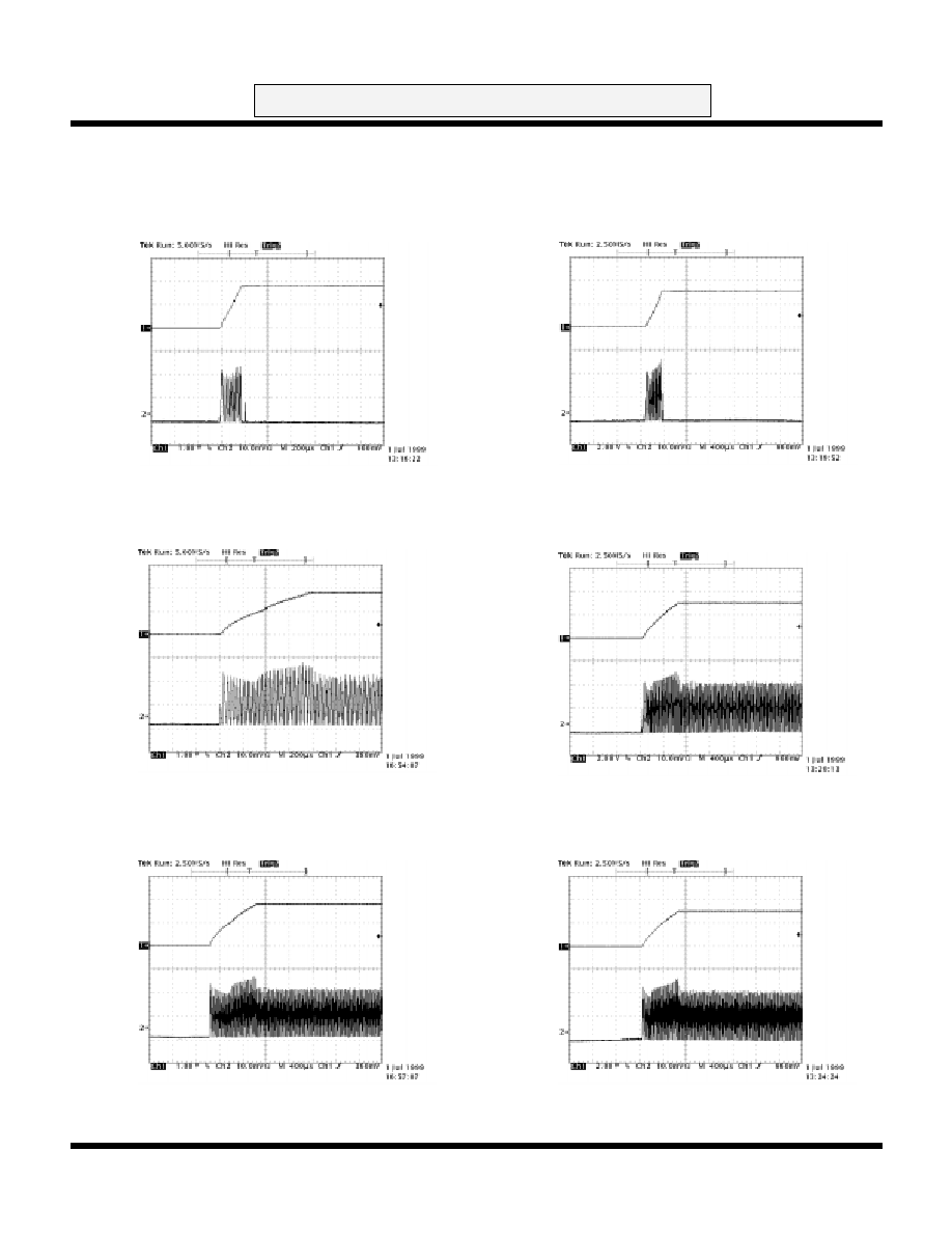
STARTUP TRANSIENT WAVEFORMS
TK65418 - Power Up No Load
Output Voltage (1V / div)
0.0V
1.8V
Inductor Current (100mA / div)
0mA
200mA
TK65433 - Power Up No Load
Output Voltage (2V / div)
0.0V
3.3V
Inductor Current (100mA / div)
0mA
200mA
TK65418 - Power Up 100mA Load
Output Voltage (1V / div)
0.0V
1.8V
Inductor Current (100mA / div)
0mA
200mA
TK65433 - Power Up 100mA Load
Output Voltage (2V / div)
0.0V
3.3V
0mA
200mA
Inductor Current (100mA / div)
TK65418 - Power Up using SB Pin (100mA Load)
Output Voltage (1V / div)
0.0V
1.8V
0mA
200mA
Inductor Current (100mA / div)
TK65433 - Power Up using SB Pin (100mA Load)
Output Voltage (2V / div)
0.0V
3.3V
0mA
200mA
Inductor Current (100mA / div)
September 1999 TOKO, Inc.
Page 9
TK654xx
ADVANCED INFORMATION
TYPICAL PERFORMANCE CHARACTERISTICS (CONT.)
TURN OFF TRANSIENT WAVEFORMS
TK65418 - Transient Load (0mA to 100mA Step)
Output Voltage (50mV / div)
0mA
200mA
Inductor Current (100mA / div)
TK65433 - Transient Load (0mA to 100mA Step)
Output Voltage (50mV / div)
0mA
200mA
Inductor Current (100mA / div)
TK65418 - Transient Load (100mA to 0mA Step)
Output Voltage (50mV / div)
0mA
200mA
Inductor Current (100mA / div)
TK65433 - Transient Load (100mA to 0mA Step)
Output Voltage (50mV / div)
0mA
200mA
Inductor Current (100mA / div)
TK65418 - Power Down using SB Pin (100mA Load)
Output Voltage (1V / div)
0.0V
1.8V
0mA
200mA
Inductor Current (100mA / div)
TK65433 - Power Down using SB Pin (100mA Load)
Output Voltage (2V / div)
0.0V
3.3V
0mA
200mA
Inductor Current (100mA / div)
LOAD TRANSIENT RESPONSE WAVEFORMS
Page 10
TK654xx
September 1999 TOKO, Inc.
ADVANCED INFORMATION
THEORY OF OPERATION
Figure 1 illustrates a circuit diagram for a simple buck
(step-down) converter. Typically, the input voltage (V
IN
) is
greater than the output voltage (V
OUT
). By modulating the
switching action of switch SW1, the output voltage (V
OUT
)
can be regulated to a constant voltage that is relatively
independent of variations in the input supply (V
IN
) or the
current load on the V
OUT
node. The TK654xx contains all
the control circuitry, logic, and power switch (SW1) for
implementing a simple step-down or "buck" converter, as
shown in Figure 1.
In general, a switching converter utilizing the TK654xx
controller will be operating in one of three states:
1. "ON" STATE: During this state of operation SW1 will be
turned on. Current through the inductive element (L) will be
increasing at a rate proportional to the voltage difference
between V
IN
and V
OUT
. In this state, there is a direct
current path from the input supply to the output load
through the inductor L.
2. "OFF" STATE: During this state of operation SW1 will
be turned off. Current through the inductive element will be
greater than zero and flowing either through the external
schottky rectifier (D) or the synchronous rectifier internal to
the TK654xx. During the "off" state, current through the
inductive element (L) will be decreasing at a rate
approximately proportional to V
OUT
. In this state, the
current drawn from the input supply is essentially zero.
Current to the load is provided by stored energy in the
inductive element.
3. "NULL" STATE: During this state of operation SW1 will
be turned off. Current through the inductive element will be
approximately zero. The internal synchronous rectifier will
be turned off. All current demands of the load will be
provided by the output filter capacitor (C). In this state, the
current drawn from the input supply is essentially zero.
Since the inductive current is zero, no additional energy is
available from the inductor. If the current demands of the
load are very light, the current will be provided by the
stored charge in the output filter capacitor. If the voltage of
the filter capacitor drops below the regulation threshold, an
"on" state will be initiated and additional energy will be
transferred from the input supply to the output.
The control scheme for the TK654xx forces the converter
to step through the "on," "off," and "null" states in sequence.
Assume that the controller is initially in the "null" state and
V
OUT
is greater than the regulation threshold. As soon as
the output voltage drops below this threshold, the controller
will switch from "null" state to the "on" state. During the "on"
state, current through inductor (L) will be increasing.
Current will flow from the input supply to the output
capacitor through the inductive element. In this state,
energy is transferred directly from the input supply to the
output through the inductor. The maximum duration of the
"on" state is inversely proportional to the difference between
the input voltage (V
IN
) and the output voltage (V
OUT
).
The transition from the "on" state to the "off" state can be
initiated by one of two different means. As mentioned
above, the maximum duration of the "on" state is inversely
proportional to the difference between the input voltage
(V
IN
) and the output voltage (V
OUT
). If the duration of the
"on" cycle exceeds this maximum, the controller
immediately switches to the "off" state independent of
other factors. Understanding that when the converter is in
a dropout condition (V
IN
V
OUT
), the maximum "on" time
is infinite and the "on" state is constantly applied. By
limiting the duration of the "on" cycle, the peak inductor
current is also being limited. The second method for
initiating the "off" cycle is triggered when the duration of the
"on" cycle exceeds a minimum on-time duration and the
output voltage (V
OUT
) exceeds the regulation threshold.
Therefore, the actual duration of the "on" cycle will vary
between a minimum on-time (T
ON(MIN)
) and a maximum
on-time (T
ON(MAX)
) depending upon the load current. At
very light loads the on-time duration will be at a minimum;
at very heavy loads the on-time will be at a maximum. This
ability to vary the duration of the on cycle is a proprietary
control scheme which can produce a ten-fold reduction in
ripple when compared to competing devices.
The transition from the "off" state to the "null" state occurs
after sufficient time has been allowed for the inductor
current to return to zero. The actual duration of the "off"
VIN
VOUT
C
D
L
SW1
+
FIGURE 1: SIMPLE "BUCK" CONVERTER
September 1999 TOKO, Inc.
Page 11
TK654xx
ADVANCED INFORMATION
THEORY OF OPERATION (CONT.)
cycle will be dependent upon the duration of the preceding
"on" cycle and the sensed input and the output voltages.
The approximate duration of the "off" cycle can be predicted
as follows:
T
OFF
= T
ON
X (V
IN
- V
OUT
) / V
OUT
During the majority of the "off" cycle, a power switch is
turned on. The turn-on point of the switch is synchronized
with the initiation of the "off" cycle. The turn-off point is near
the end of the "off" cycle. The addition of this switch
reduces the voltage drop across the external rectifying
device and provides significant improvements in converter
efficiency.
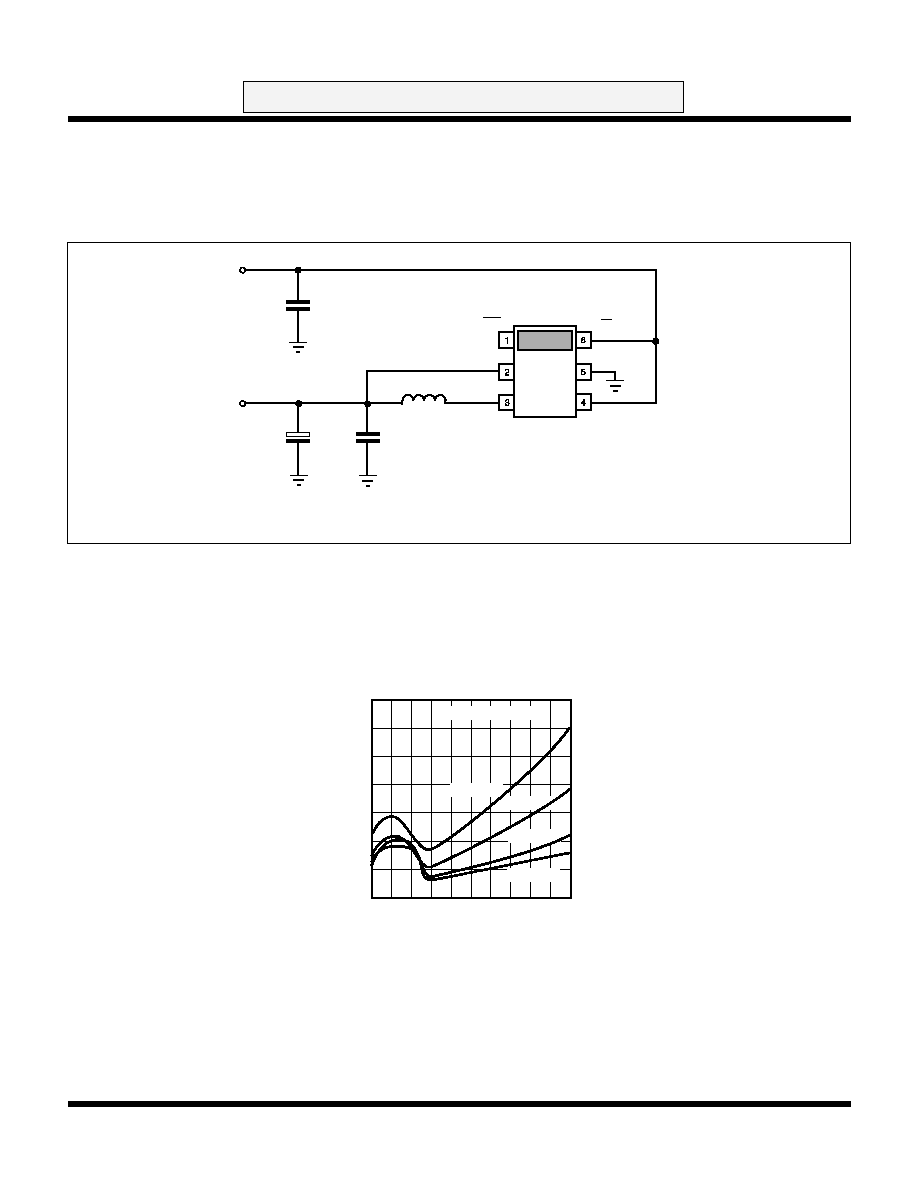
BATTERY MONITOR SECTION
In a typical voltage monitor, which uses an external resistive
divider for setting the voltage monitor threshold, the input
bias current to the monitor pin is essentially zero. In this
type of scenario, the voltage on the monitor input would be
a resistively divided version of the battery voltage. The
Battery Monitor of the TK654xx introduces a small feedback
current (-I
LBI
) which introduces a "plateau" into the transfer
characteristics between the battery voltage and the voltage
monitoring pin. The width of this plateau is dependent
upon the current range of the feedback current (-I
LBI
) and
the values of the external resistor network. Figure 2
illustrates the typical relationship between the battery
voltage (V
IN
), the feedback current (-I
LBI
) and the voltage
on the monitoring pin (V
LBI
).
In selecting a resistor divider network, there are typically
two degrees of freedom when selecting values. The first
criteria in selecting the divider is the ratio of the two
resistors. Selecting the ratio defines the upper threshold of
the voltage monitor. The second degree of freedom when
selecting the resistor divider is the absolute resistance
values. This second degree of freedom can be utilized to
set a secondary monitoring threshold (V
OFF
) lesser than
the first.
Typically, when the battery voltage is relatively high, the
voltage on the LBI input pin will be a resistively divided
version of the battery voltage.
As the battery voltage drops, the voltage on the V
LBI
pin will
drop proportionately. When the voltage on the LBI input pin
passes through approximately 1.22 V, the output of the
first comparator (LBO) will transition from a high to a low
state and the synchronous rectifier N-channel MOSFET
will stop being switched. There is about 50 mV of hysteresis
between the LBO trip point and its reset point. Shortly after
the LBO output has been asserted, as the input voltage
continues to drop, the magnitude of the current out of the
V
LBI
pin will begin to flow and proportionately increase as
the input voltage decreases. An op-amp feedback loop
internal to the Battery Monitor of the TK654xx will attempt
to maintain the voltage on the V
LBI
pin at a constant value
of approximately 1.22 V (thus, the plateau). As the battery
voltage continues to drop, there comes a point where the
feedback current stops increasing at about 720 nA. At this
point, the voltage on the LBI pin will resume a proportional
drop with the input voltage and the TK654xx converter will
turn off.
For details on how to properly select the resistor divider,
refer to the "Design Considerations" section.
FIGURE 2: BATTERY MONITOR OPERATION
GRAPHS
VLBI
LBO
OFF
1.22 V
VLBO
VOFF
VIN
720 nA
0 nA
-ILBI

Page 12
TK654xx
September 1999 TOKO, Inc.
ADVANCED INFORMATION
INPUT VOLTAGE PIN (V
IN
)
This pin is the positive input supply for the TK654xx. Current
flowing into this pin provides power to the IC and to the
converter output through the inductive element. During the
"on" state, the majority of the current flowing into this pin is
flowing through the inductor. During the "off" and "null" states,
the current into this pin is very small (approximately 18
µ
A).
The voltage source driving this pin should have relatively low
AC impedance. Good design practices dictate decoupling to
the GND pin.
GROUND PIN (GND)
This pin provides the ground connection for the IC.
OUTPUT VOLTAGE PIN (V
OUT
)
This pin senses the output voltage of the buck converter.
Input current into this pin is very low (approximately 10
µ
A).
The output voltage is resistively divided in the IC and compared
to the bandgap voltage. If the output voltage remains greater
than the regulation threshold, the TK654xx remains in a
standby state. As soon as the output voltage drops below the
regulation threshold, the TK654xx will initiate an "on" and "off"
cycle to boost the output voltage.
SW PIN
This pin is normally connected to one pin of the inductive
element and an external optional passive schottky rectifier
(optional to increase efficiency). The external schottky rectifier
is connected between this pin and ground. It is recommended
that the lead lengths between the rectifier and the pins of the
TK654xx be kept as short as possible to minimize parasitic
inductances.
LOW BATTERY INPUT/STANDBY PIN (LBI/SB)
This input pin is capable of performing two separate functions
which will be dependent upon the application's requirements.
In some applications, this input pin can be used as a Low
Battery Input (LBI). In such an application, this input pin is
typically driven by a resistively divided version of the input
supply (V
IN
). For detailed information on selecting values for
the resistor divider, please refer to Design Considerations on
pages 13 and 14.
PIN DESCRIPTION
The second function of this pin is to act as a Standby (SB)
input. If this pin is greater than approximately 1.22 V, the
converter will operate normally. Driving this pin low will force
the converter into a "standby" mode where the DC/DC
conversion is disabled. In this "standby" mode, the current
through the inductive element goes to zero; only the filter
capacitor will provide current to the output.
If neither the Low-Battery or Standby features are needed,
this input pin should be connected directly to the V
IN
pin.
Under this mode of operation, the TK654xx will not turn off. As
the input voltage approaches the regulation voltages the
TK654xx will act as a P-Channel pass element with
approximately a 2
resistance, going into the linear mode of
operation.
LOW BATTERY OUTPUT PIN (LBO)
This pin provides a Low Battery Output (LBO) signal to
indicate when the voltage on the LBI input pin has dropped
below the low battery threshold (1.22 V). This open-drain
output is normally pulled up to either the input supply or the
output supply through a resistive pull-up. The LBO output pin
provides an active-low output. If the LBO is not going to be
used, the pin may be left open.
September 1999 TOKO, Inc.
Page 13
TK654xx
ADVANCED INFORMATION
DESIGN CONSIDERATIONS
INDUCTOR SELECTION
One of the positive features of the TK654xx is the ability to
limit the magnitude of the short circuit current without the
need for external current sensing resistors. Since the
maximum on-time duration is limited, and the converter
always operates in discontinuous conduction mode (DCM),
the maximum load current is essentially dependent upon
the selection of the inductor value. The following table
defines the maximum load current as a function of the
inductor value.
OUTPUT FILTER CAPACITOR SELECTION
The purpose of the filter capacitor on the output is to
temporarily provide current to the load as inductor current
is ramping upward or downward. In general, larger
capacitors will reduce the magnitude of the ripple.
INPUT FILTER CAPACITOR SELECTION
Typically, the power supply or battery source connected to
the V
IN
pin contains an inductive and resistive component.
Since the current draw from the input supply varies with
time, such a scenario would exhibit ripple on the input
supply. Adding a bypass capacitor between the V
IN
pin
and ground, in some cases, will dramatically decrease
ripple on the input supply. An input supply bypass capacitor
in the range of 1 to 10
µ
F will work well for most converter
applications up to 100 mA. Bypass capacitors on the input
pin should exhibit relatively good ESR characteristics.
LOW BATTERY MONITOR
The TK654xx utilizes a proprietary method for sensing and
handling low battery voltages. Using a single input pin and
resistive divider, the TK654xx not only provides an early
warning system of a low battery, it also provides a later
L
MAX LOAD
47 µH
305 mA
100 µH
140 mA
220 µH
65 mA
470 µH
20 mA
R1
R2
300 k
VIN
LBO
OUTPUT
VOUT
LBO
VIN
SW
GND
LBI/SB
FIGURE 3: LOW BATTERY MONITOR
shutdown threshold which occurs at a voltage lower than
the LBI threshold. Both the LBI threshold and the shutdown
threshold can be set utilizing a single resistive divider.
For the following explanation, please refer to Figure 3.
When the battery voltage (V
IN
) is very high, the current
from the LBI input pin is essentially zero. The voltage on
the LBI input pin is simply a resistively-divided version of
the V
IN
pin.
As the voltage on the LBI input pin drops and passes
through the bandgap voltage (1.22 V), the LBI input pin will
begin to source current. At this same point, the LBO output
will be asserted. The assertion of the LBO output is
typically used as an early warning, indicating that battery
failure is approaching.
As the voltage on the V
IN
pin continues to drop, the current
sourced by the LBI input pin will continue to linearly
increase with the drop-in supply voltage. The current from
the LBI input pin will attempt to keep the voltage pin at the
same potential as the bandgap reference (1.22 V).
Throughout this region, the LBO output is continuously
asserted.
The current sourced from the LBI input pin is internally
limited to a maximum of approximately 720 nA. As
mentioned above, the current from the LBI input pin
continues to increase as the supply voltage drops. When
the current from the LBI input pin reaches the 720 nA
threshold, the TK654xx will turn off. This essentially provides
a second threshold, less than the LBI/SB threshold, where
the system will turn off.
Page 14
TK654xx
September 1999 TOKO, Inc.
ADVANCED INFORMATION
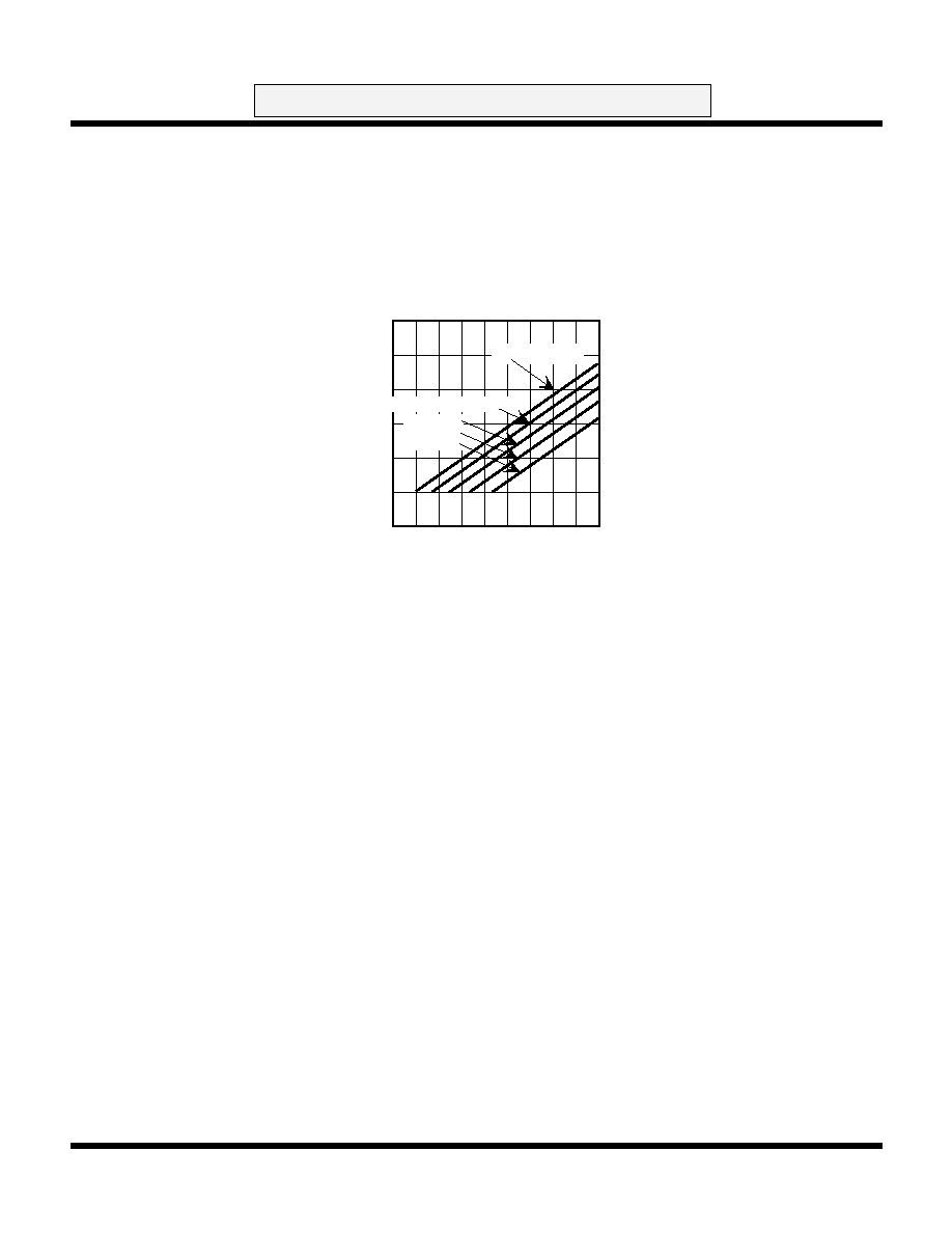
The thresholds for the Low Battery Input (LBI) and the turnoff (V
OFF
) can be set independently using a single resistive
divider. Equations and a chart for selecting the LBI and V
OFF
thresholds are provided below:
LBI threshold = 1.22 V X (R
1
+ R
2
) / R
2
V
OFF
threshold = LBI threshold - 720 nA X R
1
DROPOUT CHARACTERISTICS
In battery powered applications, the input supply is not typically a constant value. As the battery discharges, the input
voltage will approach the output voltage. As the voltage on the input of the converter drops, the following two
characteristics can be observed: (a) as the battery voltage drops, output ripple will increase, (b) at very low battery levels
and high current loads, the output voltage may drop significantly below the regulation threshold.
In some applications, the above characteristics may not present a problem. For those applications that may be sensitive
to these characteristics, the LBO output can provide an early warning system indicating that battery failure is near. As
the battery voltage continues to drop, the turnoff feature of the TK654xx will ultimately turn the converter off (see LBI
Indicator section).
RATIO OF R1/R2
0.6 1.0 1.4 1.8
3.0 V
2.0 V
4.0 V
2.5 V
3.5 V
LBI THRESHOLD
VOFF THRESHOLD (R1 = 243 K)
(R1 = 487 K)
(R1 = 732 K)
(R1 = 976 K)
LBI/V
OFF
THRESHOLD
DESIGN CONSIDERATIONS (CONT.)
September 1999 TOKO, Inc.
Page 15
TK654xx
ADVANCED INFORMATION
NOISE CONSIDERATIONS
GENERAL
Because of the switching waveforms inherent to the operation of DC-DC converters, they tend to be noisier than their
linear counterparts. A DC-DC converter uses switching techniques to do the power conversion at higher efficiencies than
a linear regulator at the price of noisier output ripple. The TK654xx is no exception to this, even though the proprietary
architecture chosen was centered in providing the user fast transient response, low quiescent current and minimum
ripple.
INPUT/OUTPUT CAPACITORS (GENERAL)
By the nature of their operation, DC-DC converters generate large switching currents on both the input and output of the
circuit. The input and output capacitors should be as large as practical with a low Equivalent Series Resistance (ESR).
Since low temperatures cause the value of capacitance to decrease and the ESR to increase, care should be taken to
select capacitors that have acceptable characteristics over the desired operating temperature range.
INPUT CAPACITOR
The function of the input capacitor is to reduce the supply impedance and to provide sufficient input current during
switching for stable circuit operation. The input capacitor should be physically located as close as posssible to the
converter to minimize the lead inductance and to reduce the impedance of the source at high frequencies. By having
the capacitor close to the converter, the switching current pulses are supplied locally by the capacitor instead of running
across the printed circuit board by long etch runs. This greatly reduces the noise on the board.
OUTPUT CAPACITOR
The function of the output capacitor is to reduce the ripple voltage appearing on the converter output. The output ripple
voltage is the AC voltage which appears on the regulated DC output. It is inherent in all DC-DC converters and is the
result of the conversion of the input DC to AC and then back to output DC. The output ripple is the result of two factors,
which are 90
∞
out of phase. The first factor is the result of the change in the stored charge of the output capacitor as it
is charged by the switching current from the converter and then discharged by the load current. This factor determines
the value (
µ
F) of the output capacitor. The second factor is the product of the capacitor's charge/discharge current times
its ESR. This factor determines the requirement for low ESR capacitors. In DC-DC converters, the ripple produced by
the capacitor ESR is often larger than the ripple produced by the change in charge. For this reason, high quality ceramic,
tantalum, or aluminum filter capacitors are required to minimize the output ripple. This contribution to output ripple and
noise can also be minimized by the addition of a small (0.01
µ
F to 0.1
µ
F) ceramic capacitor in parallel with the bulk output
capacitor. Adding a Pi filter as shown below (Figure 4) can further reduce output noise. The Pi filter has a tendency to
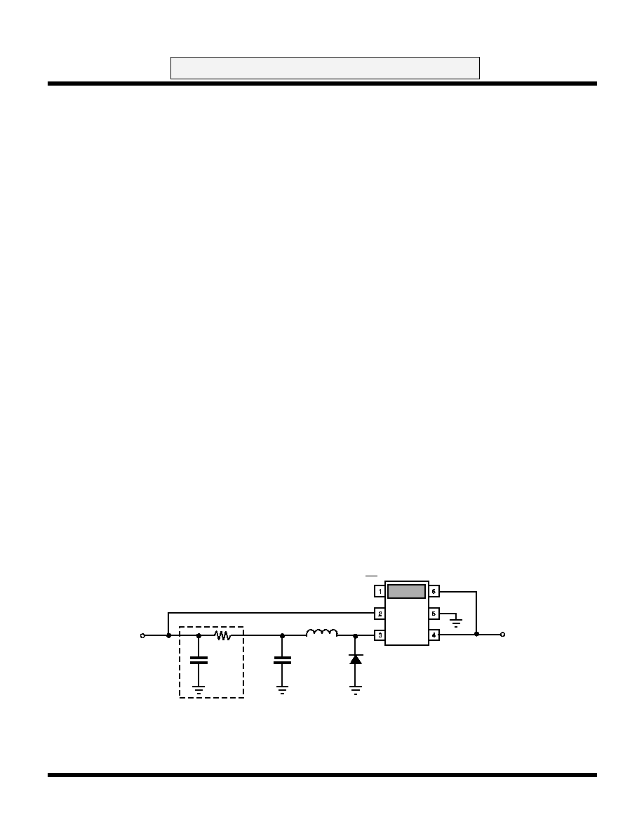
reduce the efficiency by a couple of percentage points and yet the noise improves by 20 dB/decade.
FIGURE 4: OPTIONAL PI FILTER
VOUT
C1
22 µF
L1
100 µH
LBI
GND
VIN
LBO
VOUT
SW
VIN = 5 V
OPTIONAL
FILTER
D1
LL 103
1
22 µF
Page 16
TK654xx
September 1999 TOKO, Inc.
ADVANCED INFORMATION
NOISE CONSIDERATIONS (CONT.)
COIL
The coil magnetic field can also be a source of noise. This noise is more characteristic of radiated Electromagnetic
Interference (EMI). This radiated noise can interfere with RF communications systems if care is not taken by the system
designer. A shielded coil can improve this source of EMI.
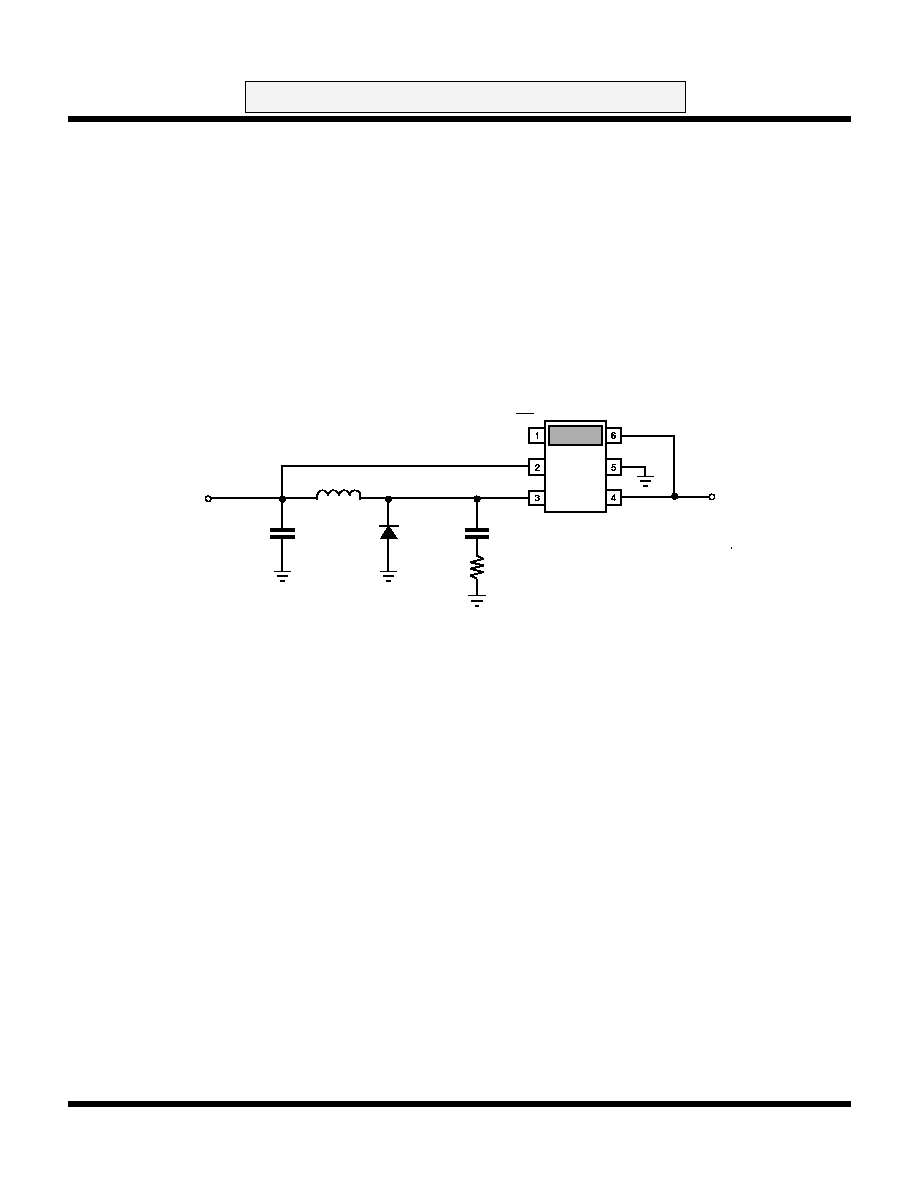
SNUBBER
When the inductor current flowing through the output diode decays to zero, the parasitic capacitance at the switch pin
(pin 3) resulting from the internal switch and external diode has energy which rings back into the inductor. This high
frequency ringing is an undesirable source of radiated noise. Fortunately, due to the low amount of energy in this ringing,
a simple RC snubber as shown in Figure 5 easily eliminates it. In low noise applications the RC snubber is recommended,
although an efficiency penalty of approzimately 2% will result.
C1
22 µF
L1
100 µH
VOUT = 3 V
LBI
GND
VIN
LBO
VOUT
SW
VIN = 5 V
D1
LL 103
220
PF
1 K
FIGURE 5: OPTIONAL SNUBBER
September 1999 TOKO, Inc.
Page 17
TK654xx
ADVANCED INFORMATION
There are several issues to consider when choosing the proper coil for the TK654xx Step-Down Converter.
An important consideration is the coil manufacturer. Toko Inc. has been in the coil business for many years and has been
a leader in this market with high quality of product, low cost, and high volume delivery distribution.
The test circuit in this data sheet uses the D10F type series for its low resistance (0.27
for 100
µ
H). This coil should
be considered when the user is interested in high efficiency.
TYPE D10F
For Reflow Soldering
Frequency Range: 1 kHz ~ 1 MHz
Inductance Range: 10 ~ 1500
µ
H
A major issue today is space as well as height. Toko makes a low profile surface mount coil series which may accomodate
this requirement. The D52 series dimensions are shown below. The 100
µ
H coil has a maximum rated DC resistance
of 1.6
.
COIL CONSIDERATIONS
Unit:mm
TYPE D52FU
Frequency Range: 1 kHz ~ 2 MHz
Inductance Range: 100
µ
H ~ 6800
µ
H
FEATURES
∑ Low profile (2.0 mm typ. height) and 5 mm square
∑ Magnetically shielded version, unshielded also available
∑ Available on tape and reel for auto insertion
∑ Suitable for reflow soldering
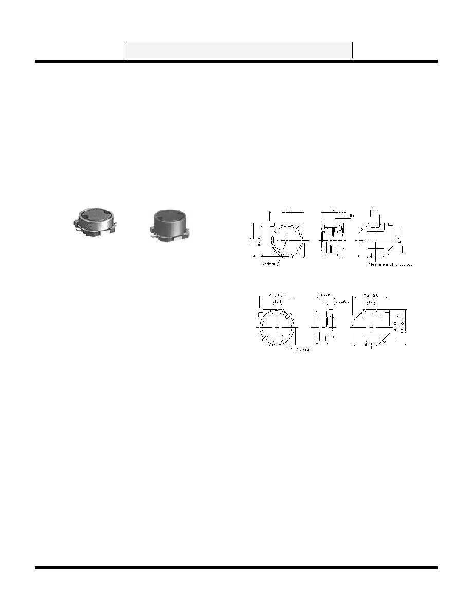
Page 18
TK654xx
September 1999 TOKO, Inc.
ADVANCED INFORMATION
TYPE D73C, D75C
For Reflow Soldering
Frequency Range: 10 kHz ~ 1 MHz
Inductance Range: 1-560
µ
H
FEATURES
∑ Miniature surface mount type
∑ Low profile (3.0 ~ 5.1 mm max height)
∑ Inductance range: 1-560
µ
H
∑ Available in magnetically shielded or unshielded versions
∑ Supplied on tape and reel for auto insertion
∑ Ideal for a variety of DC-DC Converter inductor applications
COIL CONSIDERATIONS (CONT.)
Toko makes other series of coils which fall between the D10F and D52 series.
The D73/D75 coils should be kept in mind.
D73C
D75C
Unit:mm
Unit:mm
D75
D73
September 1999 TOKO, Inc.
Page 19
TK654xx
ADVANCED INFORMATION
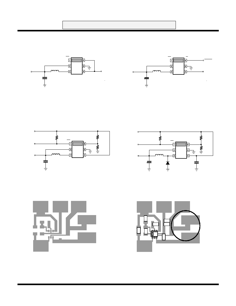
APPLICATION INFORMATION
C1
22 µF
L1
100 µH
VOUT = 3 V
LBI
GND
VIN
LBO
VOUT
SW
VIN = 5 V
FIGURE 6: MINIMUM DEVICE COUNT
C1
22 µF
L1
100 µH
VOUT = 3 V
SB
GND
VIN
LBO
VOUT
SW
VIN = 5 V
STANDBY
FIGURE 7: CONVERTER WITH STANDBY
C1
20 µF
L1
100 µH
R3
300 k
VIN = 5 V
R1
634 K
R2
287 K
LBI
GND
VIN
LBO
VOUT
SW
VOUT = 3 V
LB OUT
C2
10 µF
D
1
(optional)
FIGURE 9: EVALUATION BOARD SCHEMATIC
FIGURE 9B: EVALUATION BOARD ARTWORK
V
OUT
GND
LBO
V
IN
FIGURE 8: LOW BATTERY DETECTOR
C1
22 µF
L1
100 µH
R3
300 k
VIN = 5 V
R1
634 K
R2
287 K
LBI
GND
VIN
LBO
VOUT
SW
VOUT = 3 V
LB OUT
FIGURE 9C: EVALUATION BOARD COMPONENT
PLACEMENT
V
OUT
GND
LBO
V
IN
R3
R2
C2
C1
C1
L1
R1
*
D1
*D1 Optional
Page 20
TK654xx
September 1999 TOKO, Inc.
ADVANCED INFORMATION
APPLICATION INFORMATION (CONT.)
The portable market, computing market and communications market, appear to not only be growing very fast, but also to
be converging.
Whether a computer incorporates communications capability or the phone incorporates the data / file transfer capability,
both markets as we approach the next millenium certainly are portable and require high efficiencies as well as long standby
times in order to extend the battery life. As the user gets more and more comfortable with his portable system, he will want
longer and longer time before recharging the battery.
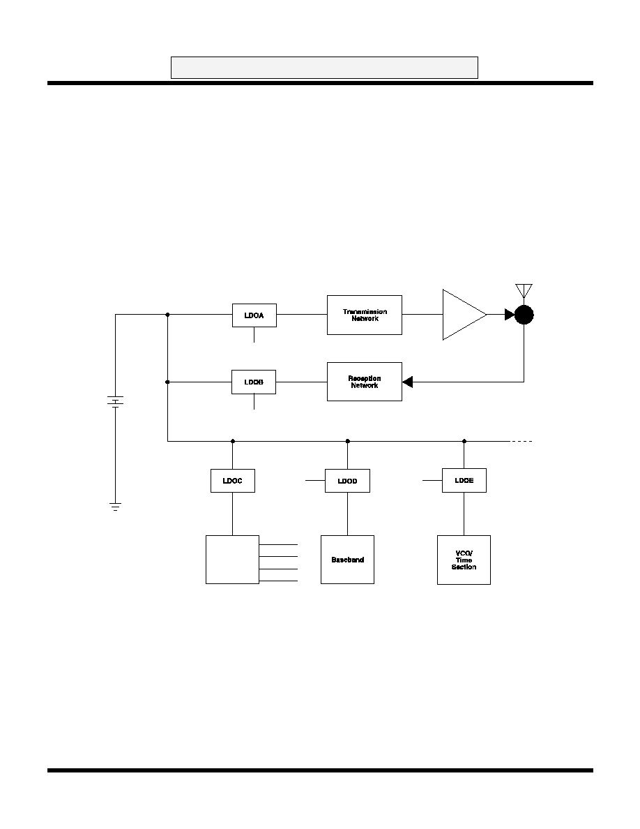
WIRELESS PORTABLE SYSTEM USING LINEAR REGULATORS
FIGURE 10: Linear regulators power up wireless application
Power
Amp
Enable A
Enable B
Enable A
Enable B
Enable D
Enable E
Enable D
Enable E
µ Controller
September 1999 TOKO, Inc.
Page 21
TK654xx
ADVANCED INFORMATION
APPLICATION INFORMATION (CONT.)
New microprocessors are earnestly addressing this power issue by reducing the voltage. Battery manufacturers are
waking up right before the end of the century with the introduction of the "polymer electrolyte battery" which allows for higher
volumetric and gravimetric densities. Furthermore, these types of batteries come with much better form factors.
Unfortunately the wireless transmit and receive section of the portable system is very sensitive and requires very clean
analog voltages to keep a clean reception and transmission. This RF requirement reigns over the power management
section of the system and creates a dilemma to the system engineer. How do you extend the battery life with "efficient
switchers" when they are so "dirty" in performance compared to "linears"?
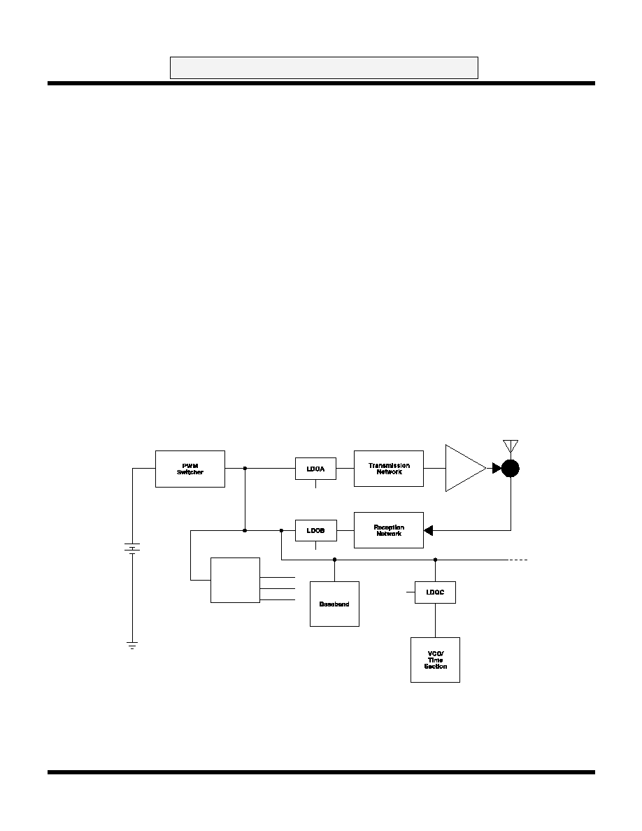
The industry has made attempts to get away from a sole linear system shown in Fig. 10 by considering a "PWM" switcher
in front of the linear as shown if Fig. 11.
The system of Fig. 10 has the advantage of very clean voltages for the RF section, but lacks high efficiency. Specifically
as the processor voltage drops and the battery makers refine the Li-Polimer battery (which ranges from 2.7V min to 4.2V
max).
The system of Fig. 11 has the advantage of high efficiency followed by clean RF due to the linears, but lacks the ability
to turn off (turn on) fast when the system is in standby operation. This is specifically due to the PWM architecture which
uses Continuous Conduction Mode (CCM) to build up the current in the coil.
WIRELESS PORTABLE SYSTEM USING PWM SWITCHER TO IMPROVE EFFICIENCY
FIGURE 11: PWM Switcher embedded to improve wireless system efficiency
Power
Amp
Enable A
Enable B
Enable C
µ Controller
Enable A
Enable B
Enable C
Page 22
TK654xx
September 1999 TOKO, Inc.
ADVANCED INFORMATION
APPLICATION INFORMATION (CONT.)
The industry is presently in a frame of mind that unless the switcher is PWM with a fixed frequency (to fix the harmonics
away from the RF), the wireless RF section will not be clean. It is the intention of this application to open the mind of system
designers to consider this new concept which addresses a real issue. Several major IC manufacturers of PWM step down
converters are taunting the "Burst Mode" capability. This can be misleading since under the burst mode, the fixed
frequency of the PWM is no longer present. (Therefore harmonics are all over the place). Furthermore, the purpose of
the Burst Mode is to allow the system to go into a standby mode in order to save battery life. Yet these state of the art PWMs
with Burst mode ability still lack in response time due to the architecture which requires the coil current to slowly build up.
This build up in current is a barrier to the present day requirements.
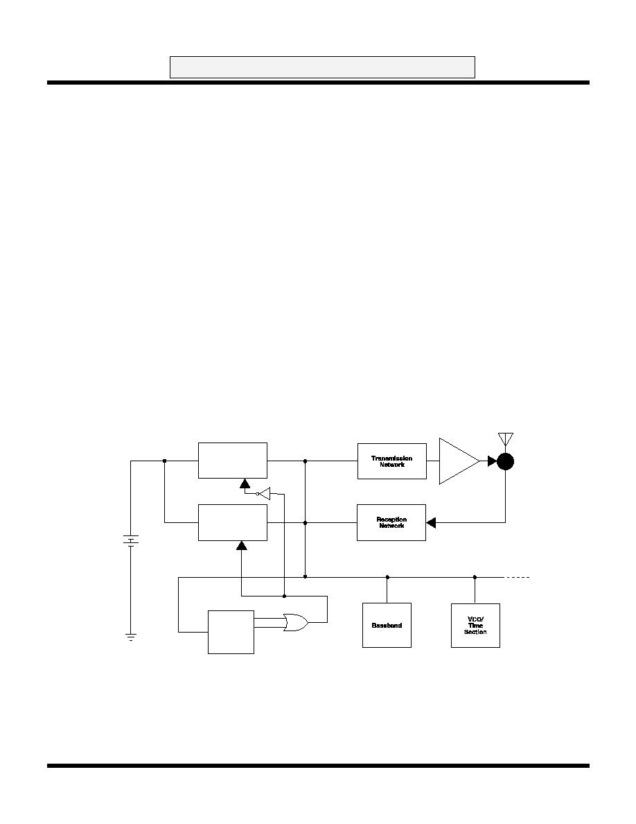
This Buck and Linear Wireless application proposes a system as shown in Fig. 12, which allows for all 3 important aspects
of the design:
1)
Clean RF
2)
High efficiency (At full, mid, and light loads)
3)
Low standby currents with fast "wake up" response.
The approach shown in Fig. 12 requires a new architecture for the Buck (Step down) switching converter with very fast
transient characteristics, specifically during the transition from a Buck mode to Linear mode while a RF transmission/
reception is eminent or during a wake up out of standby mode.
WIRELESS PORTABLE SYSTEM USING BUCK AND LINEAR REGULATORS
FIGURE 12: Buck and Linear embedded to improve wireless system efficiency, standy time, and clean RF
Power
Amp
Transmit
Receive
µ Controller
Buck
Enable
Buck
Enable
Linear
LDO
Linear
*
* Not necessary if LDO is active low

September 1999 TOKO, Inc.
Page 23
TK654xx
ADVANCED INFORMATION
APPLICATION INFORMATION (CONT.)
Toko Inc. has come up with such a proprietary architecture implemented in their TK654XX switching step down converter.
This device is full of features as itemized in the following section:
TK654XX Features
1)
Minimum pin count. Only 6 pins in a SOT23L package
2)
Minimum external components required:
Coil and Filter cap
3)
Synchronous Rectification
4)
Extremely low operating current (25uA).
5)
18uA Standby Currents
6)
Internal power devices good for greater than 200mA loads
7)
Inherent short circuit protection
8)
No instabilities
9)
Fast transient response
10)
High efficiencies up to 95%
11)
Regulation down to 1.8V
12)
Proprietary architecture specifically aims at low ripple voltage.
13)
Low Dropout operation (100% Duty Cycle)
14)
Designed for battery operated equipment
15)
Battery Monitor included
16)
Easy to design with (Reduce the coil to increase the load current)
Explanation of Figs. 10, 11, 12 follows:
Figure 10, shows a battery operated system with communications capability. The microcontroller is programmed to turn
on / off the Linear Low Dropout regulators (LDOs) at the appropriate time. This enabling capability is useful in extending
the battery life. Please note the LDO C, which powers the microcontroller is always active.
Figure 11, takes advantage of LDO C having to be active continuously and replaces it with a PWM step down controller.
Though the PWM is always active like the LDO C of Figure 10, the PWM is more efficient and therefore is penetrating the
Wireless market in order to increase battery life. It must be pointed out in Figure 11, the role of the LDOs is important to
maintain the clean voltages for Transmission and reception modes. Figure 11 also points out that if there is small activity
with the microcontroller which controls the other LDOs, the system could trip to the "Burst Mode" taunted by semiconductor
manufacturers. This mode is intended to reduce the current consumption of the PWM and
increase
the overall battery
life. Unfortunately, the speed that this Burst mode-to-PWM mode can react in is not very fast. Those systems, which are
compromised to increase response time, will inevitably hurt in ripple and therefore noise performance.
Figure 12, replaces the PWM with a Buck (step down) converter which has a unique architecture to respond very fast from
"Burst mode" to full load operation and a linear in parallel, rather than in series which can be enabled at the time the system
requires to transmit or receive. It is only due to the clean RF that the LDO is necessary. The majority of the time these
wireless systems are in a mode which can operate with some noise in the main voltage line. Some readers may have
noticed that Figure 12 only requires 1 LDO versus 3 LDOs in Figure 11. This principal may point out that the overall system
may turn out to be more cost effective. The system shown in Figure 12, therefore not only extends the overall battery life
by allowing the system to go into standby modes where the overall current is in the order of 25 uA, but at full load can run
in the 95% efficiency (no Transmission / Receive mode). Figure 12 can maintain the clean RF requirements for wireless
communications and reduce the overall cost.
Page 24
TK654xx
September 1999 TOKO, Inc.
ADVANCED INFORMATION
SB
GND
TK11330
VIN
VOUT
VOUT
VIN
GND
SW
100 µH
Transmit/
Receive
10 µF
Control
GND
Noise
Bypass
1000 pF
VIN
3.0 V
LBO
Note A
TK11330
TK65430
SB
GND
TK11330
VIN
VOUT
VOUT
VIN
GND
SW
100 µH
Transmit/
Receive
10 µF
Control
GND
Noise
Bypass
1000 pF
VIN
3.0 V
LBO
Note A
TK11330
TK65430
100 µF
Note B
APPLICATION INFORMATION (CONT.)
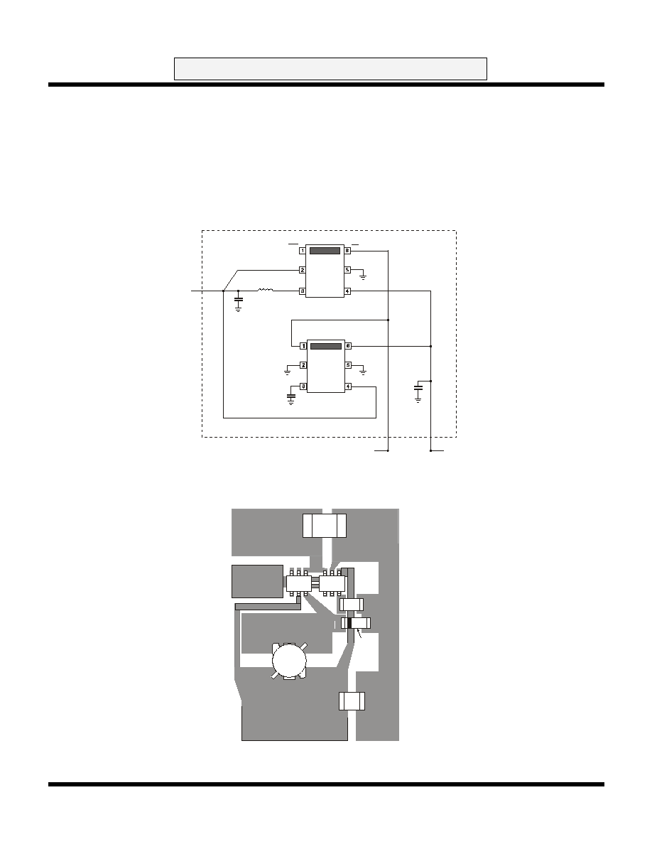
FIGURE 13: BUCK AND LINEAR SCHEMATIC
FIGURE 14: BUCK AND LINEAR APPLICATION BOARD LAYOUT
Wireless Application Extend battery life, yet keep RF clean
Application results with waveforms for TK65430 in a Buck and Linear Mode
Figure 13 is a schematic of an application board available from Toko as APO14-99 from which the results shown
below were obtained. This application uses the TK11330 Low Dropout Regulator with the control function enabling
the regulator on when this control pin is low.
AP014-99
TOKO
V
IN
GND
CON
V
OUT
TK113xxBM
1
TK654xx
1
D1
CIN
CN
1000pF
875FU-xxxM
CL
Optional
10 µF
100 µF
Note A: This is a low ESR
(80 m
) capacitor from
AVX TPSD107 M010R0080
Note B: Coil used to obtain
waveforms was D63LCB type
A921CY-101M from Toko
September 1999 TOKO, Inc.
Page 25
TK654xx
ADVANCED INFORMATION
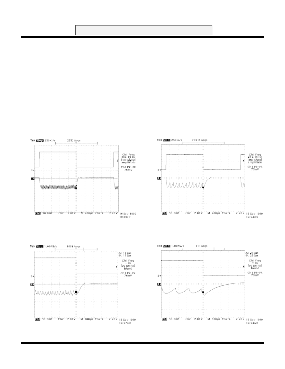
APPLICATION INFORMATION (CONT.)
V
IN
= 5 V I
OUT
= 100 mA
Full Cycle
Switching to Linear
During the transient response between the "Buck" and "Linear" control modes the output voltage needs to stay within
the regulation requirements.
The following scope pictures show the changes in the output voltage during these transients. As can be seen, the
maximum drop is about 80 mV and maximum overshoot is negligible.
In switching from the "Buck" mode to the "Linear" mode the settling time is less than 250
µ
sec over the supply range
of 5 V to 3.2 V for this 3.0 V application.
TK65430 in a Buck and Linear Mode
V
IN
= 3.2 V I
OUT
= 100 mA
Full Cycle
Switching to Linear
Page 26
TK654xx
September 1999 TOKO, Inc.
ADVANCED INFORMATION
APPLICATION INFORMATION (CONT.)
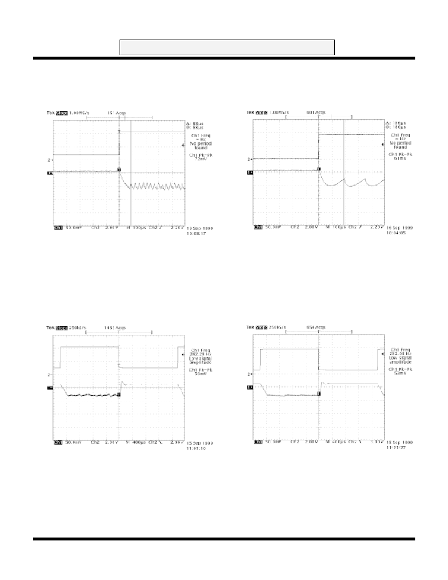
In conclusion, the ability to provide a clean signal during transmission/reception can be done with linear regulators in a
predictable way, the novelty comes in considering the Buck and Linear concept which has the advantage of high
efficiency while not compromising the linear regulator's low noise characteristics.
The overall effect being longer battery life while maintaining low RF interference in a wireless system.
V
IN
= 5 V I
OUT
= 100 mA
V
IN
= 3.2 V I
OUT
= 100 mA
Switching to Buck
Switching to Buck
V
IN
= 5 V I
OUT
= 20 mA
V
IN
= 3.2 V I
OUT
= 20 mA
Full Cycle
Full Cycle
Characteristics of this application under lighter loads but similar supply range are shown below.

September 1999 TOKO, Inc.
Page 27
TK654xx
ADVANCED INFORMATION
NOTES
Page 28
TK654xx
September 1999 TOKO, Inc.
ADVANCED INFORMATION
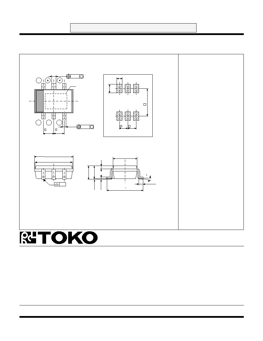
0.95
0.95
0.32
e
e
M
0.1
+0.15
- 0.05
3.5
1.2
0.15
0.3
3.3
2.2
0.4
0.95
0.95
3.0
e
e
e1
0.6
1.0
Recommended Mount Pad
1
2
3
6
0 - 0.1
15 max
1.4 max
Marking
+0.3
- 0.1
+ 0.3
(3.4)
+0.15
- 0.05
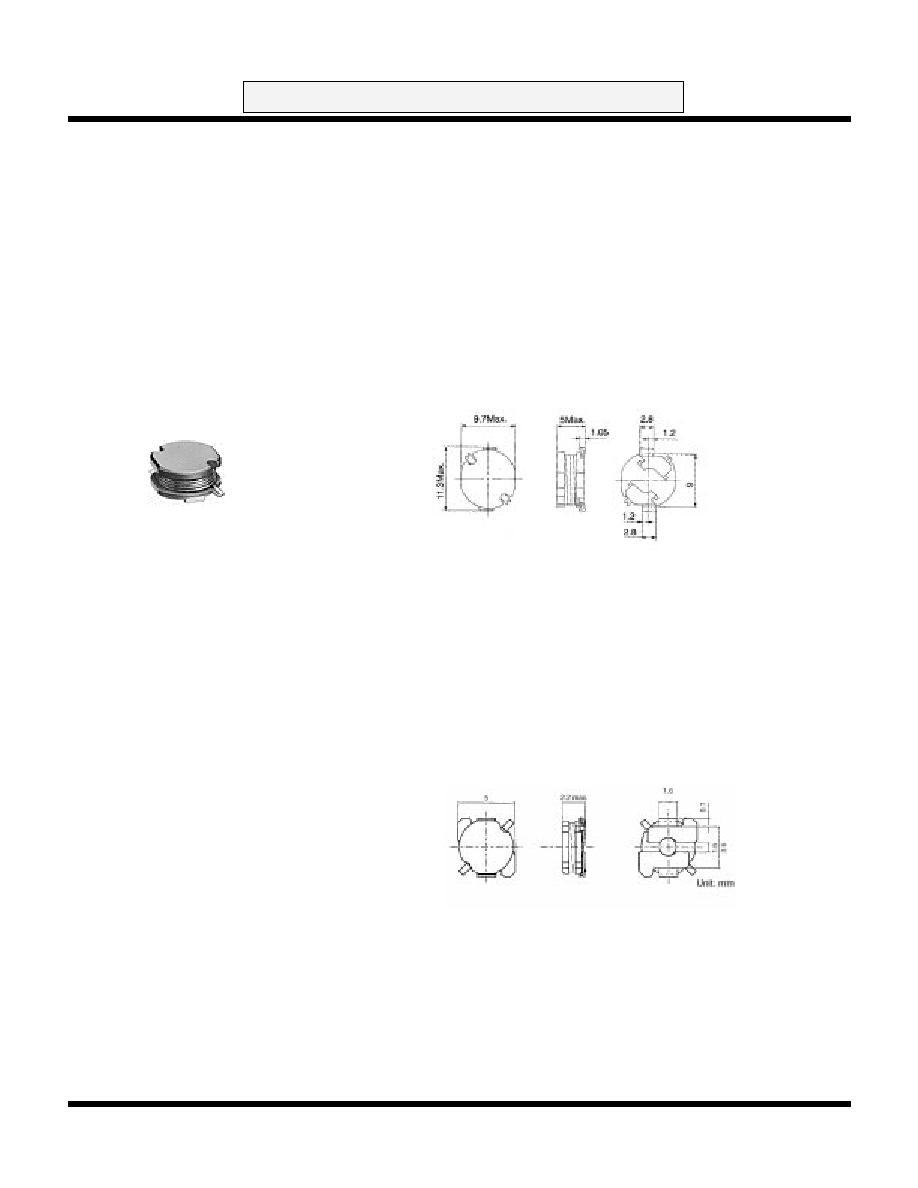
Dimensions are shown in millimeters
Tolerance: x.x =
±
0.2 mm (unless otherwise specified)
0.1
M
0.1
+0.15
- 0.05
0.4
Marking Information
Marking
TK65418
418
*TK65419
419
*TK65420
420
TK65421
421
*TK65422
422
*TK65423
423
TK65424
424
TK65425
425
*TK65426
426
TK65427
427
*TK65428
428
*TK65429
429
TK65430
430
*TK65431
431
*TK65432
432
TK65433
433
* These voltages available upon request
SOT23L-6
PACKAGE OUTLINE
Printed in the USA
© 1999 Toko, Inc.
All Rights Reserved
TOKO AMERICA REGIONAL OFFICES
Toko America, Inc. Headquarters
1250 Feehanville Drive, Mount Prospect, Illinois 60056
Tel: (847) 297-0070 Fax: (847) 699-7864
IC-260-TK654xx
0899O0.0K
Visit our Internet site at http://www.tokoam.com
The information furnished by TOKO, Inc. is believed to be accurate and reliable. However, TOKO reserves the right to make changes or improvements in the design, specification or manufacture of its
products without further notice. TOKO does not assume any liability arising from the application or use of any product or circuit described herein, nor for any infringements of patents or other rights of
third parties which may result from the use of its products. No license is granted by implication or otherwise under any patent or patent rights of TOKO, Inc.
Western Regional Office
Toko America, Inc.
2480 North First Street , Suite 260
San Jose, CA 95131
Tel: (408) 432-8281
Fax: (408) 943-9790
Midwest Regional Office
Toko America, Inc.
1250 Feehanville Drive
Mount Prospect, IL 60056
Tel: (847) 297-0070
Fax: (847) 699-7864
Eastern Regional Office
Toko America, Inc.
107 Mill Plain Road
Danbury, CT 06811
Tel: (203) 748-6871
Fax: (203) 797-1223
Semiconductor Technical Support
Toko Design Center
4755 Forge Road
Colorado Springs, CO 80907
Tel: (719) 528-2200
Fax: (719) 528-2375