
December 1999 TOKO, Inc.
Page 1
TK716xx
FEATURES
s
Available in
±
2.0 % or
±
1.0 % Output Tolerance
s
Active High On/Off Control
s
Very Low Quiescent Current
s
Very Low Dropout Voltage
s
Reverse Bias Protection
s
Miniature Package (SOT23-5)
s
Short Circuit Switch
s
High Ripple Rejection
s
Very High Output Impedance (Output Off)
s
Very Low Noise
BLOCK DIAGRAM
TK716xx
20P
GND
VIN
NOISE
BYPASS
VOUT
CONTROL
CONTROL
GND
VIN
VOUT
BANDGAP
REFERENCE
CONSTANT
CURRENT
SOURCE
THERMAL AND
OVERCURRENT
PROTECTION
DISCONNECT
CIRCUIT
NOISE
BYPASS
+
-
CONTROL
CIRCUIT
TK716 SCL
TK716 S I L
TK716 SCL H
ORDERING INFORMATION
TAPE/REEL CODE
L: Tape Left
TEMPERATURE CODE
C: Standard Temp. Range
I: Extended Temp. Range
PACKAGE CODE
S: SOT23-5
TOLERANCE CODE
H: 1 % Output Voltage Tolerance
(Not available in I temp code)
CAPACITOR CODE
None: Ceramic Capacitor
A: Tantalum Capacitor
Tape/Reel Code
Voltage Code
Temp. Code
Package Code
VOLTAGE CODE*
13 = 1.3 V
14 = 1.4 V
15 = 1.5 V
16 = 1.6 V
17 = 1.7 V
18 = 1.8 V
19 = 1.9 V
20 = 2.0 V
21 = 2.1 V
22 = 2.2 V
23 = 2.3 V
24 = 2.4 V
25 = 2.5 V
26 = 2.6 V
Tolerance Code
Capacitor Code
27 = 2.7 V
28 = 2.8 V
29 = 2.9 V
30 = 3.0 V
31 = 3.1 V
32 = 3.2 V
33 = 3.3 V
34 = 3.4 V
35 = 3.5 V
36 = 3.6 V
37 = 3.7 V
38 = 3.8 V
39 = 3.9 V
40 = 4.0 V
41 = 4.1 V
42 = 4.2 V
43 = 4.3 V
44 = 4.4 V
45 = 4.5 V
46 = 4.6 V
47 = 4.7 V
48 = 4.8 V
49 = 4.9 V
50 = 5.0 V
51 = 5.1 V
52 = 5.2 V
53 = 5.3 V
54 = 5.4 V
*Check Table 4
for availability.
DESCRIPTION
The TK716xx is a low dropout linear regulator housed in a
small SOT23-5 package, rated at 500 mW. The phase
compensation in the IC has been optimized to allow the
use of ceramic or tantalum output capacitors. The device
is in the "on" state when the control pin is pulled to a logic
high level. An internal PNP pass transistor is used to
achieve a low dropout voltage of 90 mV (typ.) at 50 mA
load current. This device offers high precision output
voltage of
±
2.0 % or
±
1.0 %. The low quiescent current
and dropout voltage make this part ideal for battery pow-
ered applications. This part incorporates an output discon-
nect feature to reduce the reverse bias current in the "off"
state to less than 50 nA.
APPLICATIONS
s
Battery Powered Systems
s
Cellular Telephones
s
Pagers
s
Personal Communications Equipment
s
Portable Instrumentation
s
Portable Consumer Equipment
s
Radio Control Systems
s
Toys
s
Low Voltage Systems
LOW DROPOUT VOLTAGE REGULATOR
The internal reverse bias protection eliminates the require-
ment for a reverse voltage protection diode, saving cost
and board space. The high 60 dB ripple rejection (400 Hz)
and low noise provide enhanced performance for critical
applications. An external capacitor can be connected to
the noise bypass pin to lower the output noise level to 30
µ
Vrms.
Page 2
December 1999 TOKO, Inc.
TK716xx
ABSOLUTE MAXIMUM RATINGS
Supply Voltage ......................................................... 16 V
Power Dissipation (Note 1) ................................ 500 mW
Reverse Bias Voltage ................................................. 6 V
Control Terminal Voltage ......................................... 12 V
Noise Bypass Terminal Voltage ................................. 5 V
Operating Voltage Range ............................... 1.8 to 12 V
Storage Temperature Range ................... -55 to +150
∞
C
Operating Temperature (Ambient) Range
TK716xx SCL, TK716xx SCLH ............ -30 to +80
∞
C
TK716xx SIL .......................................... -40 to +85
∞
C
Junction Temperature (Operating) ........................ 125
∞
C
Junction Temperature (Shutdown) ........................ 150
∞
C
Lead Soldering Temperature (10 s) ...................... 235
∞
C
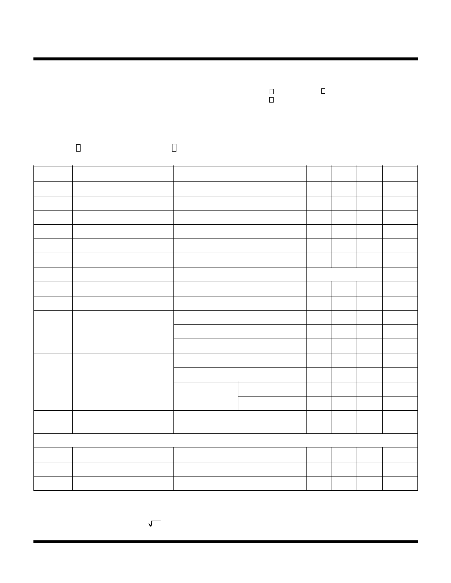
TK716xx SCL AND TK716xx SCLH ELECTRICAL CHARACTERISTICS
Test conditions: V
IN
= V
OUT(TYP)
+ 1 V, T
A
= 25
∞
C, unless otherwise specified.
Note 1: Power dissipation is 500 mW when mounted as recommended. Derate at 4.0 mW/
∞
C for operation above 25
∞
C.
Gen Note: Exceeding the "Absolute Maximum Ratings" may damage the device.
Gen Note: Parameters with min. or max. values are 100% tested at T
A
= 25
∞
C.
Gen Note:
Ripple rejection is @ 60 dB when f = 400 Hz, C
L
= 10
µ
F, C
N
= 0.1
µ
F, input noise = 100 mVrms, V
IN
= V
OUT(TYP)
+ 1.5 V and I
OUT
= 30 mA.
Gen Note: Output noise is 0.13 ~ 0.23
µ
V/ Hz at 1 kHz when C
N
= 0.1
µ
F.
L
O
B
M
Y
S
R
E
T
E
M
A
R
A
P
S
N
O
I
T
I
D
N
O
C
T
S
E
T
N
I
M
P
Y
T
X
A
M
S
T
I
N
U
I
Q
t
n
e
r
r
u
C
t
n
e
c
s
e
i
u
Q
I
T
U
O
I
g
n
i
d
u
l
c
x
E
,
A
m
0
=
T
N
O
C
0
7
0
0
1
A
µ
I
Y
B
T
S
t
n
e
r
r
u
C
y
b
d
n
a
t
S
V
N
I
,
V
8
=
V
(
F
F
O
t
u
p
t
u
O
T
N
O
C
)
V
5
1
.
0
1
.
0
A
µ
I
V
E
R
t
n
e
r
r
u
C
s
a
i
B
e
s
r
e
v
e
R
V
N
I
,
V
0
=
V
V
E
R
F
F
O
t
u
p
t
u
O
,
V
5
=
1
0
5
A
n
I
D
N
G
t
n
e
r
r
u
C
n
i
P
D
N
G
I
T
U
O
A
m
0
5
=
1
8
.
1
A
m
I
T
U
O
t
n
e
r
r
u
C
t
u
p
t
u
O
s
u
o
u
n
i
t
n
o
C
0
5
1
A
m
I
)
E
S
L
U
P
(
T
U
O
t
n
e
r
r
u
C
t
u
p
t
u
O
e
s
l
u
P
%
0
4
=
e
l
c
y
C
y
t
u
D
,
e
s
l
u
p
s
m
0
1
0
0
2
A
m
V
T
U
O
e
g
a
t
l
o
V
t
u
p
t
u
O
V
N
I
V
=
)
P
Y
T
(
T
U
O
,
V
1
+
I
T
U
O
A
m
5
=
2
d
n
a
1
e
l
b
a
T
e
e
S
V
V
T
U
O
/
T
e
r
u
t
a
r
e
p
m
e
T
t
n
e
i
c
i
f
f
e
o
C
0
2
C
∞
/
m
p
p
g
e
R
e
n
i
L
n
o
i
t
a
l
u
g
e
R
e
n
i
L
V
N
I
V
=
)
P
Y
T
(
T
U
O
V
o
t
V
1
+
)
P
Y
T
(
T
U
O
V
6
+
2
5
1
V
m
g
e
R
d
a
o
L
n
o
i
t
a
l
u
g
e
R
d
a
o
L
I
<
A
m
1
T
U
O
A
m
0
5
<
4
8
1
V
m
I
<
A
m
1
T
U
O
A
m
0
0
1
<
7
8
2
V
m
I
<
A
m
1
T
U
O
A
m
0
5
1
<
2
1
0
5
V
m
V
P
O
R
D
e
g
a
t
l
o
V
t
u
o
p
o
r
D
I
T
U
O
A
m
0
5
=
0
9
0
6
1
V
m
I
T
U
O
A
m
0
0
1
=
0
4
1
0
3
2
V
m
I
T
U
O
A
m
0
5
1
=
V
T
U
O
V
4
.
2
0
0
2
0
0
3
V
m
V
T
U
O
V
4
.
2
<
0
0
2
0
5
3
V
m
V
f
e
r
l
a
n
i
m
r
e
T
s
s
a
p
y
B
e
s
i
o
N
e
g
a
t
l
o
V
6
2
.
1
V
S
N
O
I
T
A
C
I
F
I
C
E
P
S
L
A
N
I
M
R
E
T
L
O
R
T
N
O
C
I
T
N
O
C
t
n
e
r
r
u
C
l
o
r
t
n
o
C
V
T
U
O
,
V
6
.
1
=
N
O
t
u
p
t
u
O
0
1
A
µ
V
)
N
O
(
T
N
O
C
N
O
e
g
a
t
l
o
V
l
o
r
t
n
o
C
N
O
t
u
p
t
u
O
6
.
1
V
V
)
F
F
O
(
T
N
O
C
F
F
O
e
g
a
t
l
o
V
l
o
r
t
n
o
C
F
F
O
t
u
p
t
u
O
6
.
0
V
December 1999 TOKO, Inc.
Page 3
TK716xx
TK716xx SCL ELECTRICAL CHARACTERISTICS TABLE 1
Test Conditions: V
IN
= V
OUT(TYP)
+ 1 V, I
OUT
= 5 mA, T
A
= 25
∞
C, unless otherwise specified.
TK716xx SCLH ELECTRICAL CHARACTERISTICS TABLE 2
Test Conditions: V
IN
= V
OUT(TYP)
+ 1 V, I
OUT
= 5 mA, T
A
= 25
∞
C, unless otherwise specified.
Output
Voltage
V
OUT(MIN)
V
OUT(MAX)
Voltage
Code
1.3 V
13
1.240 V
1.360 V
1.4 V
14
1.340 V
1.460 V
1.5 V
15
1.440 V
1.560 V
1.6 V
16
1.540 V
1.660 V
1.7 V
17
1.650 V
1.760 V
1.8 V
18
1.740 V
1.860 V
1.9 V
19
1.870 V
1.960 V
2.0 V
20
1.940 V
2.060 V
2.1 V
21
2.040 V
2.160 V
2.2 V
22
2.140 V
2.260 V
2.3 V
23
2.240 V
2.360 V
2.4 V
24
2.340 V
2.460 V
2.5 V
25
2.440 V
2.560 V
2.6 V
26
2.540 V
2.660 V
2.7 V
27
2.640 V
2.760 V
2.8 V
28
2.740 V
2.860 V
2.9 V
29
2.840 V
2.960 V
3.0 V
30
2.940 V
3.060 V
3.1 V
31
3.038 V
3.162 V
3.2 V
32
3.136 V
3.264 V
3.3 V
33
3.234 V
3.366 V
Output
Voltage
V
OUT(MIN)
V
OUT(MAX)
Voltage
Code
3.8 V
38
3.760 V
3.840 V
3.9 V
39
3.860 V
3.940 V
4.0 V
40
3.960 V
4.040 V
4.1 V
41
4.059 V
4.141 V
4.2 V
42
4.158 V
4.242 V
4.3 V
43
4.247 V
4.343 V
4.4 V
44
4.356 V
4.444 V
4.5 V
45
4.455 V
4.545 V
4.6 V
46
4.554 V
4.646 V
4.7 V
47
4.653 V
4.747 V
4.8 V
48
4.752 V
4.848 V
4.9 V
49
4.851 V
4.949 V
5.0 V
50
4.950 V
5.050 V
5.1 V
51
5.049 V
5.151 V
5.2 V
52
5.148 V
5.252 V
5.3 V
53
5.247 V
5.353 V
5.4 V
54
5.346 V
5.454 V
Output
Voltage
V
OUT(MIN)
V
OUT(MAX)
Voltage
Code
3.4 V
34
3.232 V
3.468 V
3.5 V
35
3.430 V
3.570 V
3.6 V
36
3.528 V
3.672 V
3.7 V
37
3.626 V
3.774 V
3.8 V
38
3.724 V
3.876 V
3.9 V
39
3.822 V
3.978 V
4.0 V
40
3.920 V
4.080 V
4.1 V
41
4.018 V
4.182 V
4.2 V
42
4.116 V
4.284 V
4.3 V
43
4.214 V
4.386 V
4.4 V
44
4.312 V
4.488 V
4.5 V
45
4.410 V
4.590 V
4.6 V
46
4.508 V
4.692 V
4.7 V
47
4.606 V
4.794 V
4.8 V
48
4.704 V
4.896 V
4.9 V
49
4.802 V
5.008 V
5.0 V
50
4.900 V
5.100 V
5.1 V
51
4.998 V
5.202 V
5.2 V
52
5.096 V
5.304 V
5.3 V
53
5.194 V
5.406 V
5.4 V
54
5.292 V
5.508 V
Output
Voltage
V
OUT(MIN)
V
OUT(MAX)
Voltage
Code
2.0 V
20
1.960 V
2.040 V
2.1 V
21
2.060 V
2.140 V
2.2 V
22
2.160 V
2.240 V
2.3 V
23
2.260 V
2.340 V
2.4 V
24
2.360 V
2.440 V
2.5 V
25
2.460 V
2.540 V
2.6 V
26
2.560 V
2.640 V
2.7 V
27
2.660 V
2.740 V
2.8 V
28
2.760 V
2.840 V
2.9 V
29
2.860 V
2.940 V
3.0 V
30
2.960 V
3.040 V
3.1 V
31
3.060 V
3.140 V
3.2 V
32
3.160 V
3.240 V
3.3 V
33
3.260 V
3.340 V
3.4 V
34
3.360 V
3.440 V
3.5 V
35
3.460 V
3.540 V
3.6 V
36
3.560 V
3.640 V
3.7 V
37
3.660 V
3.740 V
Page 4
December 1999 TOKO, Inc.
TK716xx
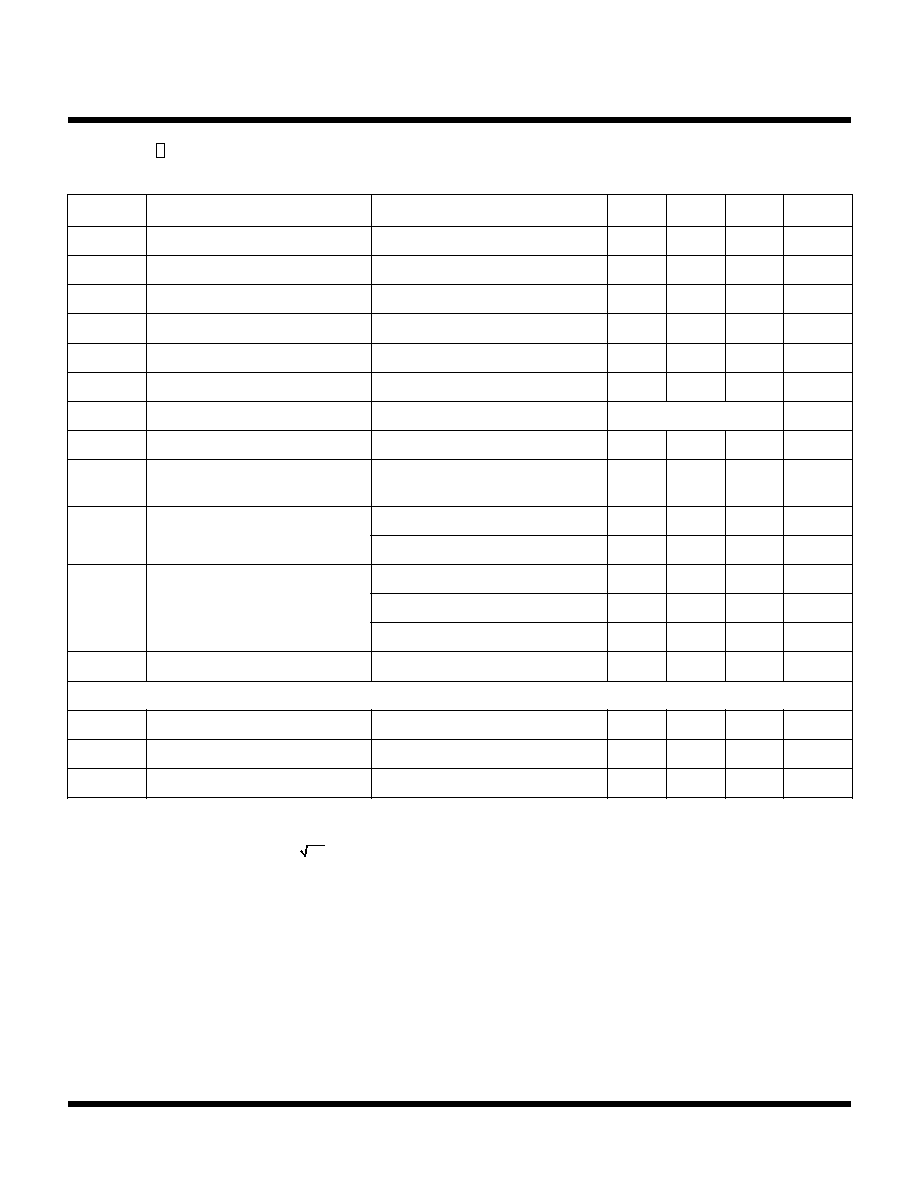
TK716xx SIL ELECTRICAL CHARACTERISTICS
Test conditions: V
IN
= V
OUT(TYP)
+ 1 V, T
A
= 25
∞
C, unless otherwise specified.
Gen Note: Exceeding the "Absolute Maximum Ratings" may damage the device.
Gen Note: Parameters with min. or max. values are 100% tested at T
A
= 25
∞
C.
Gen Note:
Ripple rejection is @ 60 dB when f = 400 Hz, C
L
= 10
µ
F, C
N
= 0.1
µ
F, input noise = 100 mVrms, V
IN
= V
OUT(TYP)
+ 1.5 V and I
OUT
= 30 mA.
Gen Note: Output noise is 0.13 ~ 0.23
µ
V/ Hz at 1 kHz when C
N
= 0.1
µ
F.
L
O
B
M
Y
S
R
E
T
E
M
A
R
A
P
S
N
O
I
T
I
D
N
O
C
T
S
E
T
N
I
M
P
Y
T
X
A
M
S
T
I
N
U
I
Q
t
n
e
r
r
u
C
t
n
e
c
s
e
i
u
Q
I
T
U
O
I
g
n
i
d
u
l
c
x
E
,
A
m
0
=
T
N
O
C
0
7
0
0
1
A
µ
I
Y
B
T
S
t
n
e
r
r
u
C
y
b
d
n
a
t
S
V
N
I
,
V
8
=
F
F
O
t
u
p
t
u
O
2
.
0
A
µ
I
V
E
R
t
n
e
r
r
u
C
s
a
i
B
e
s
r
e
v
e
R
V
N
I
,
V
0
=
V
V
E
R
F
F
O
t
u
p
t
u
O
,
V
5
=
1
0
7
A
n
I
D
N
G
t
n
e
r
r
u
C
n
i
P
D
N
G
I
T
U
O
A
m
0
5
=
1
0
.
2
A
m
I
T
U
O
t
n
e
r
r
u
C
t
u
p
t
u
O
s
u
o
u
n
i
t
n
o
C
0
5
1
A
m
I
)
E
S
L
U
P
(
T
U
O
t
n
e
r
r
u
C
t
u
p
t
u
O
e
s
l
u
P
%
0
4
=
e
l
c
y
C
y
t
u
D
,
e
s
l
u
p
s
m
0
1
0
0
2
A
m
V
T
U
O
e
g
a
t
l
o
V
t
u
p
t
u
O
V
N
I
V
=
)
P
Y
T
(
T
U
O
,
V
1
+
I
T
U
O
A
m
5
=
3
e
l
b
a
T
e
e
S
V
V
T
U
O
/
T
e
r
u
t
a
r
e
p
m
e
T
t
n
e
i
c
i
f
f
e
o
C
0
2
C
∞
/
m
p
p
g
e
R
e
n
i
L
n
o
i
t
a
l
u
g
e
R
e
n
i
L
V
N
I
V
=
)
P
Y
T
(
T
U
O
o
t
V
1
+
V
)
P
Y
T
(
T
U
O
V
6
+
2
7
1
V
m
g
e
R
d
a
o
L
n
o
i
t
a
l
u
g
e
R
d
a
o
L
I
<
A
m
1
T
U
O
A
m
0
5
<
4
0
2
V
m
I
<
A
m
1
T
U
O
A
m
0
0
1
<
7
0
3
V
m
V
P
O
R
D
e
g
a
t
l
o
V
t
u
o
p
o
r
D
I
T
U
O
A
m
0
5
=
0
9
0
6
1
V
m
I
T
U
O
A
m
0
0
1
=
0
5
1
0
4
2
V
m
I
T
U
O
A
m
0
5
1
=
0
0
2
0
1
3
V
m
V
f
e
r
e
g
a
t
l
o
V
l
a
n
i
m
r
e
T
s
s
a
p
y
B
e
s
i
o
N
6
2
.
1
V
S
N
O
I
T
A
C
I
F
I
C
E
P
S
L
A
N
I
M
R
E
T
L
O
R
T
N
O
C
I
T
N
O
C
t
n
e
r
r
u
C
l
o
r
t
n
o
C
V
T
U
O
,
V
6
.
1
=
N
O
t
u
p
t
u
O
0
1
A
µ
V
)
N
O
(
T
N
O
C
N
O
e
g
a
t
l
o
V
l
o
r
t
n
o
C
N
O
t
u
p
t
u
O
8
.
1
V
V
)
F
F
O
(
T
N
O
C
F
F
O
e
g
a
t
l
o
V
l
o
r
t
n
o
C
F
F
O
t
u
p
t
u
O
4
.
0
V
December 1999 TOKO, Inc.
Page 5
TK716xx
TK716xx SIL ELECTRICAL CHARACTERISTICS TABLE 3
Test Conditions: V
IN
= V
OUT(TYP)
+ 1 V, I
OUT
= 5 mA, T
A
= 25
∞
C, unless otherwise specified.
Room Temp. Range (T
A
= 25
∞
C) Full Temp. Range (T
A
= -40 to +85
∞
C)
Output
Voltage
V
OUT(MIN)
V
OUT(MAX)
V
OUT(MIN)
V
OUT(MAX)
Voltage
Code
2.4 V
24
2.360 V
2.440 V
2.320 V
2.480 V
2.5 V
25
2.460 V
2.540 V
2.420 V
2.580 V
2.6 V
26
2.560 V
2.640 V
2.520 V
2.680 V
2.7 V
27
2.660 V
2.740 V
2.620 V
2.780 V
2.8 V
28
2.760 V
2.840 V
2.720 V
2.880 V
2.9 V
29
2.860 V
2.940 V
2.820 V
2.980 V
3.0 V
30
2.960 V
3.040 V
3.920 V
3.080 V
3.1 V
31
3.060 V
3.140 V
3.020 V
3.180 V
3.2 V
32
3.160 V
3.240 V
3.120 V
3.280 V
3.3 V
33
3.260 V
3.340 V
3.220 V
3.380 V
3.4 V
34
3.360 V
3.440 V
3.320 V
3.480 V
3.5 V
35
3.460 V
3.540 V
3.420 V
3.580 V
3.6 V
36
3.560 V
3.640 V
3.520 V
3.680 V
3.7 V
37
3.660 V
3.740 V
3.620 V
3.780 V
3.8 V
38
3.760 V
3.840 V
3.720 V
3.880 V
3.9 V
39
3.860 V
3.940 V
3.820 V
3.980 V
4.0 V
40
3.960 V
4.040 V
3.920 V
4.090 V
4.1 V
41
4.059 V
4.141 V
4.009 V
4.191 V
4.2 V
42
4.158 V
4.242 V
4.108 V
4.292 V
4.3 V
43
4.257 V
4.343 V
4.197 V
4.893 V
4.4 V
44
4.356 V
4.444 V
4.306 V
4.494 V
4.5 V
45
4.455 V
4.545 V
4.405 V
4.595 V
4.6 V
46
4.554 V
4.646 V
4.504 V
4.496 V
4.7 V
47
4.653 V
4.747 V
4.603 V
4.497 V
4.8 V
48
4.752 V
4.848 V
4.702 V
4.898 V
4.9 V
49
4.851 V
5.049 V
4.801 V
5.099 V
5.0 V
50
4.950 V
5.050 V
4.900 V
5.100 V
Page 6
December 1999 TOKO, Inc.
TK716xx
VOLTAGE AVAILABILITY TABLE 4
Output
TK716xxSCL
TK716xxASCL
TK716xxSCLH
TK716ASCLH
TK716xxSIL
TK716xxASIL
Voltage
1.3 V
X
1.4 V
X
1.5 V
X
X
1.6 V
X
1.7 V
X
1.8 V
X
X
1.9 V
X
2.0 V
X
X
X
X
2.1 V
X
X
X
X
2.2 V
X
X
X
X
2.3 V
X
X
2.4 V
X
X
X
X
X
X
2.5 V
X
X
X
X
X
X
2.6 V
X
X
X
2.7 V
X
X
X
X
X
X
2.8 V
X
X
X
X
X
X
2.9 V
X
X
X
X
X
X
3.0 V
X
X
X
X
X
X
3.1 V
X
X
X
X
X
X
3.2 V
X
X
X
X
X
X
3.3 V
X
X
X
X
X
X
3.4 V
X
X
X
3.5 V
X
X
X
X
X
X
3.6 V
X
X
X
X
X
X
3.7 V
X
X
X
3.8 V
X
X
X
X
X
X
3.9 V
X
X
X
4.0 V
X
X
X
4.1 V
X
X
X
X
X
X
4.2 V
X
X
X
X
X
X
4.3 V
X
X
X
4.4 V
X
X
X
4.5 V
X
X
X
X
X
X
4.6 V
X
X
X
4.7 V
X
X
X
X
X
X
4.8 V
X
X
X
X
X
X
4.9 V
X
X
X
X
X
X
5.0 V
X
X
X
X
X
X
5.1 V
X
X
5.2 V
X
X
5.3 V
X
X
5.4 V
X
X
Note: X denotes voltage presently available. Consult factory for availability of other voltages.

December 1999 TOKO, Inc.
Page 7
TK716xx
IR
LEAK
(
n
A)
4
REVERSE LEAKAGE CURRENT
VS.
TEMPERATURE
TA (
∞
C)
0 25 50 75 100
0
2
VIN, VCONT FLOATING
VOUT = 5 V SOURCE
3
1
TYPICAL PERFORMANCE CHARACTERISTICS
TEST CIRCUIT
ICONT
CL = 3.3 µF
VCONT
VIN
+
+
CIN = 1.0 µF
+
IIN
VOUT
IOUT
VOUT
VIN
CONT
CN = 0.01 µF
GND
NOISE BYPASS
V
OUT
(5 mV/ DIV)
LOAD REGULATION
IOUT (mA)
0 50 100 150
VOUT TYPICAL
V
OUT
(V)
3
5
SHORT CIRCUIT PROTECTION
IOUT (mA)
1
0 150 300
4
2
0
V
OUT
(50
m
V/
DIV)
LINE REGULATION
VIN (V)
0 10 20
VOUT TYPICAL
V
DROP
(
m
V)
-100
0
DROPOUT VOLTAGE
VS.
OUTPUT CURRENT
IOUT (mA)
-200
0 100 200
-50
-150
-250
V
OUT
(20 mV/ DIV)
OUTPUT VOLTAGE
VS
.
INPUT VOLTAGE
VIN (50 MV/DIV)
0 VIN = VOUT
VOUT TYPICAL
IOUT = 150 mA
IOUT = 0 mA
IOUT = 25 mA
IOUT is changed
by 25 mA step.

Page 8
December 1999 TOKO, Inc.
TK716xx
TYPICAL PERFORMANCE CHARACTERISTICS (CONT.)
I GND
(
m
A)
4
GROUND CURRENT
TA (
∞
C)
2
-50 0 50 100
0
IOUT = 60 mA
IOUT = 30 mA
IOUT = 90 mA
STANDBY CURRENT
VS.
INPUT VOLTAGE
VIN (V)
I STBY
(A)
0 10 20
IE-10
IE-9
IE-8
IE-7
IE-11
IE-12
QUIESCENT CURRENT (ON MODE)
VS.
INPUT VOLTAGE
VIN (V)
I Q
(mA)
0 10 20
1.0
2.0
0
IOUT = 0 mA
VOUT = 3 V
VOUT = 4 V
VOUT = 5 V
REVERSE BIAS CURRENT
(VIN = 0 V)
VREV (V)
I REV (A)
0 5 10
IE-12
IE-9
IE-6
IE-3
CONTROL CURRENT (ON MODE)
VS.
CONTROL PIN VOLTAGE
VCONT(V)
I CONT
(µA)
0 2.5 5
2.5
5.0
0
IOUT = 0 mA
VOUT
REVERSE BIAS CURRENT
VS.
TEMPERATURE (VIN = 0 V)
TA (
∞
C)
I REV (A)
0 25 50 75 100
IE-12
IE-9
IE-6
IE-3
December 1999 TOKO, Inc.
Page 9
TK716xx
V
DROP
(
m
V)
200
DROPOUT VOLTAGE
TA (
∞
C)
150
-50 0 50 100
0
100
50
IOUT = 60 mA
IOUT = 150 mA
IOUT = 1mA
IOUT = 90 mA
IOUT = 30 mA
I CONT
(
µ
A)
5
CONTROL CURRENT
TA (
∞
C)
4
-50 0 50 100
0
3
2
1
VCONT = 3.3 V
VCONT = 1.8 V
I OUT
(
m
A)
340
MAXIMUM OUTPUT CURRENT
TA (
∞
C)
-50 0 50 100
260
300
320
280
TYPICAL PERFORMANCE CHARACTERISTICS (CONT.)
OUTPUT NOISE DENSITY
f (Hz)
NOISE (µV/ H
Z
)
100 I K 10 K 100 K
1.0
10
0
IOUT = 30 mA
CL = 2.2 µF
CNP = 0.001 µF
0.1
CNP = 0.01 µF
CNP = 0.1 µF
RIPPLE REJECTION
0.01 0.1 1 10 100
f (kHz)
-80
RR (dB)
-20
-60
-40
0
-100
IOUT =30 mA
CL = 3.3 µF
CN = 0.01 µF
CL = 3.3 µF
CN = 0.1 µF
V
OUT
/
T
(ppm)
10
OUTPUT VOLTAGE TEMPERATURE
COEFFICIENT
TA (
∞
C)
-50 0 50 100
-30
-10
0
-20
VOUT = 3 V
Page 10
December 1999 TOKO, Inc.
TK716xx
LOAD CURRENT STEP RESPONSE 1
TIME (2.5 µs/ DIV)
I OUT
V
OUT
V
OUT (20 mV/ DIV)
CN = 0.01 µF, CL = 2.2 µF
IOUT = 0 to 30 mA
IOUT = 30 to 60 mA
IOUT = 5 to 35 mA
LINE VOLTAGE STEP RESPONSE 1
TIME (50 µs/ DIV)
V
IN
V
OUT
CN = 0.01 µF, CL = 2.2 µF
V
OUT
V
OUT (10 mV/ DIV)
CN = 0.001 µF, CL = 2.2 µF
VOUT +1 V
VOUT +2 V
LINE VOLTAGE STEP RESPONSE 2
TIME (50 µs/ DIV)
V
IN
V
OUT
CN = 0.01 µF, CL = 10 µF
V
OUT
V
OUT (10 mV/ DIV)
CN = 0.01 µF, CL = 3.3 µF
VOUT +1 V
VOUT +2 V
V
CONT
OUTPUT VOLTAGE RESPONSE 2
(OFF ~ ON)
TIME (µs)
0 200 400 600 800
V
OUT
CN = 1000 pF
CN = 0.1 µF
CN = 0.01 µF
ILOAD = 30 mA, CL = 3.3 µF
V
CONT
OUTPUT VOLTAGE RESPONSE 1
(OFF ~ ON)
TIME (µs)
0 20 40 60 80
V
OUT
CL = 2.2 µF
CL = 3.3 µF
CL = 10 µF
ILOAD = 10 mA, CN = 1000 pF
CL = 4.7 µF
TYPICAL PERFORMANCE CHARACTERISTICS (CONT.)
NOISE
(
µ
V)
250
NOISE LEVEL
VS.
CN
CN
1 pF 10 pF 100 pF 1000 pF 0.01 µF 0.1 µF
50
150
200
100
0
CL = 2.2 µF
CL = 3.3 µF
CL = 10 µF
December 1999 TOKO, Inc.
Page 11
TK716xx
TYPICAL PERFORMANCE CHARACTERISTICS (CONT.)
LOAD CURRENT STEP RESPONSE 2
TIME (2.5 µs/ DIV)
I OUT
V
OUT
V
OUT (20 mV/ DIV)
CN = 0.01 µF, CL = 2.2 µF
IOUT = 60 to 30 mA
IOUT = 30 to 0 mA
IOUT = 35 to 5 mA
CONTROL VOLTAGE
VS.
TEMPERATURE
TA (
∞
C)
V
CONT
(V)
0 25 50 75 100
1.5
2.0
0
1.0
0.5
OUTPUT ON
OUTPUT OFF
SHORT CIRCUIT CURRENT
VS.
INPUT VOLTAGE
VIN (V)
I OUT
(mA)
0 2 4 6 8
300
400
0
200
100
VOUT IS CONNECTED TO GND
CONTROL CURRENT
VS.
TEMPERATURE
TA (
∞
C)
I CONT
(µ
A)
0 25 50 75 100
4.0
5.0
0
3.0
2.0
VCONT = 5.0 V
1.0
VCONT = 2.0 V
DROPOUT CHARACTERISTICS
VIN (1 V/ DIV)
V
OUT
(0
.
5
V/
DIV)
IOUT = 80 mA
IOUT = 0 mA
VIN = VOUT
VOUT
GROUND CURRENT
VS.
OUTPUT CURRENT
IOUT (mA)
I GND
(mA)
0 0.9 40 50 120 160 200
30
40
0
20
10

Page 12
December 1999 TOKO, Inc.
TK716xx
GROUND CURRENT
VS.
INPUT
SUPPLY VOLTAGE (VOUT = 3.6 V)
VIN (V)
I GND
(mA)
0 1 2 3 4 5
3
4
0
2
1
IOUT= 50 mA
IOUT = 0 mA
GROUND CURRENT
VS.
TEMPERATURE
TA (
∞
C)
I GND
(mA)
0 25 50 75 100
3
4
0
2
1
IOUT = 80 mA
IOUT = 50 mA
IOUT = 0 mA
I SC
(
m
A)
400
INSTANTANEOUS SHORT CIRCUIT
CURRENT
VS.
TEMPERATURE
TA (
∞
C)
0 25 50 75 100
0
200
VIN = VOUT +1
CL = 2.2 µF TANTALUM
300
100
TYPICAL PERFORMANCE CHARACTERISTICS (CONT.)

December 1999 TOKO, Inc.
Page 13
TK716xx
DEFINITION AND EXPLANATION OF TECHNICAL TERMS
OUTPUT VOLTAGE (V
OUT
)
The output voltage is specified with V
IN
= (V
OUT(TYP)
+ 1 V)
and I
OUT
= 5 mA.
DROPOUT VOLTAGE (V
DROP
)
The dropout voltage is the difference between the input
voltage and the output voltage at which point the regulator
starts to fall out of regulation. Below this value, the output
voltage will fall as the input voltage is reduced. It is
dependent upon the load current and the junction
temperature.
CONTINUOUS OUTPUT CURRENT (I
OUT
)
Normal operating output current. This is limited by package
power dissipation.
PULSE OUTPUT CURRENT (I
OUT (PULSE)
)
Maximum pulse width 10 ms; duty cycle is 40%: pulse load
only.
LINE REGULATION (Line Reg)
Line regulation is the ability of the regulator to maintain a
constant output voltage as the input voltage changes. The
line regulation is specified as the input voltage is changed
from V
IN
= V
OUT
+ 1 V to V
IN
= V
OUT
+ 6 V.
LOAD REGULATION (Load Reg)
Load regulation is the ability of the regulator to maintain a
constant output voltage as the load current changes. It is
a pulsed measurement to minimize temperature effects
with the input voltage set to V
IN
= V
OUT
+1 V. The load
regulation is specified under three output current step
conditions of 1 mA to 50 mA, 1 mA to 100 mA and 1 mA to
150 mA.
QUIESCENT CURRENT (I
Q
)
The quiescent current is the current which flows through
the ground terminal under no load conditions (I
OUT
= 0 mA).
GROUND CURRENT (I
GND
)
Ground Current is the current which flows through the
ground pin(s). It is defined as I
IN
- I
OUT
, excluding control
current.
RIPPLE REJECTION RATIO (RR)
Ripple rejection is the ability of the regulator to attenuate
the ripple content of the input voltage at the output. It is
specified with 100 mVrms, 400 Hz superimposed on the
input voltage, where V
IN
= V
OUT
+ 1.5 V. The output
decoupling capacitor is set to 10
µ
F, the noise bypass
capacitor is set to 0.1
µ
F, and the load current is set to
30 mA. Ripple rejection is the ratio of the ripple content of
the output vs. the input and is expressed in dB.
STANDBY CURRENT (I
STBY
)
Standby current is the current which flows into the regulator
when the output is turned off by the control function
(V
CONT
= 0 V). It is measured with V
IN
= 8 V.
SENSOR CIRCUITS
Overcurrent Sensor
The overcurrent sensor protects the device if the output is
shorted to ground.
Thermal Sensor
The thermal sensor protects the device if the junction
temperature exceeds the safe value (T
j
= 150
∞
C). This
temperature rise can be caused by extreme heat, excessive
power dissipation caused by large output voltage drops, or
excessive output current. The regulator will shut off when
the temperature exceeds the safe value. As the junction
temperature decreases, the regulator will begin to operate
again. Under sustained fault conditions, the regulator
output will oscillate as the device turns off then resets.
Damage may occur to the device under extreme fault
conditions.
Reverse Voltage Protection
Reverse voltage protection prevents damage due to the
output voltage being higher than the input voltage. This
fault condition can occur when the output capacitor remains
charged and the input is reduced to zero, or when an
external voltage higher than the input voltage is applied to
the output side.
Page 14
December 1999 TOKO, Inc.
TK716xx
DEFINITION AND EXPLANATION OF TECHNICAL TERMS (CONT.)
PACKAGE POWER DISSIPATION (P
D
)
This is the power dissipation level at which the thermal
sensor is activated. The IC contains an internal thermal
sensor which monitors the junction temperature. When the
junction temperature exceeds the monitor threshold of
150
∞
C, the IC is shut down. The junction temperature
rises as the difference between the input power (V
IN
x I
IN
)
and the output power (V
OUT
x I
OUT
) increases. The rate of
temperature rise is greatly affected by the mounting pad
configuration on the PCB, the board material, and the
ambient temperature. When the IC mounting has good
thermal conductivity, the junction temperature will be low
even if the power dissipation is great. When mounted on
the recommended mounting pad, the power dissipation of
the SOT23-5 is increased to 500 mW. For operation at
ambient temperatures over 25
∞
C, the power dissipation of
the SOT23-5 device should be derated at 4.0 mW/
∞
C. To
determine the power dissipation for shutdown when
mounted, attach the device on the actual PCB and
deliberately increase the output current (or raise the input
voltage) until the thermal protection circuit is activated.
Calculate the power dissipation of the device by subtracting
the output power from the input power. These
measurements should allow for the ambient temperature
of the PCB. The value obtained from P
D
/(150
∞
C - T
A
) is the
derating factor. The PCB mounting pad should provide
maximum thermal conductivity in order to maintain low
device temperatures. As a general rule, the lower the
temperature, the better the reliability of the device. The
thermal resistance when mounted is expressed as follows:
T
j
= 0
jA
x P
D
+ T
A
For Toko ICs, the internal limit for junction temperature is
150
∞
C. If the ambient temperature (T
A
) is 25
∞
C, then:
150
∞
C = 0
jA
x P
D
+ 25
∞
C
0
jA
= 125
∞
C / P
D
P
D
is the value when the thermal protection circuit is
activated. A simple way to determine P
D
is to calculate V
IN
x I
IN
when the output side is shorted. Input current gradually
falls as temperature rises. You should use the value when
thermal equilibrium is reached.
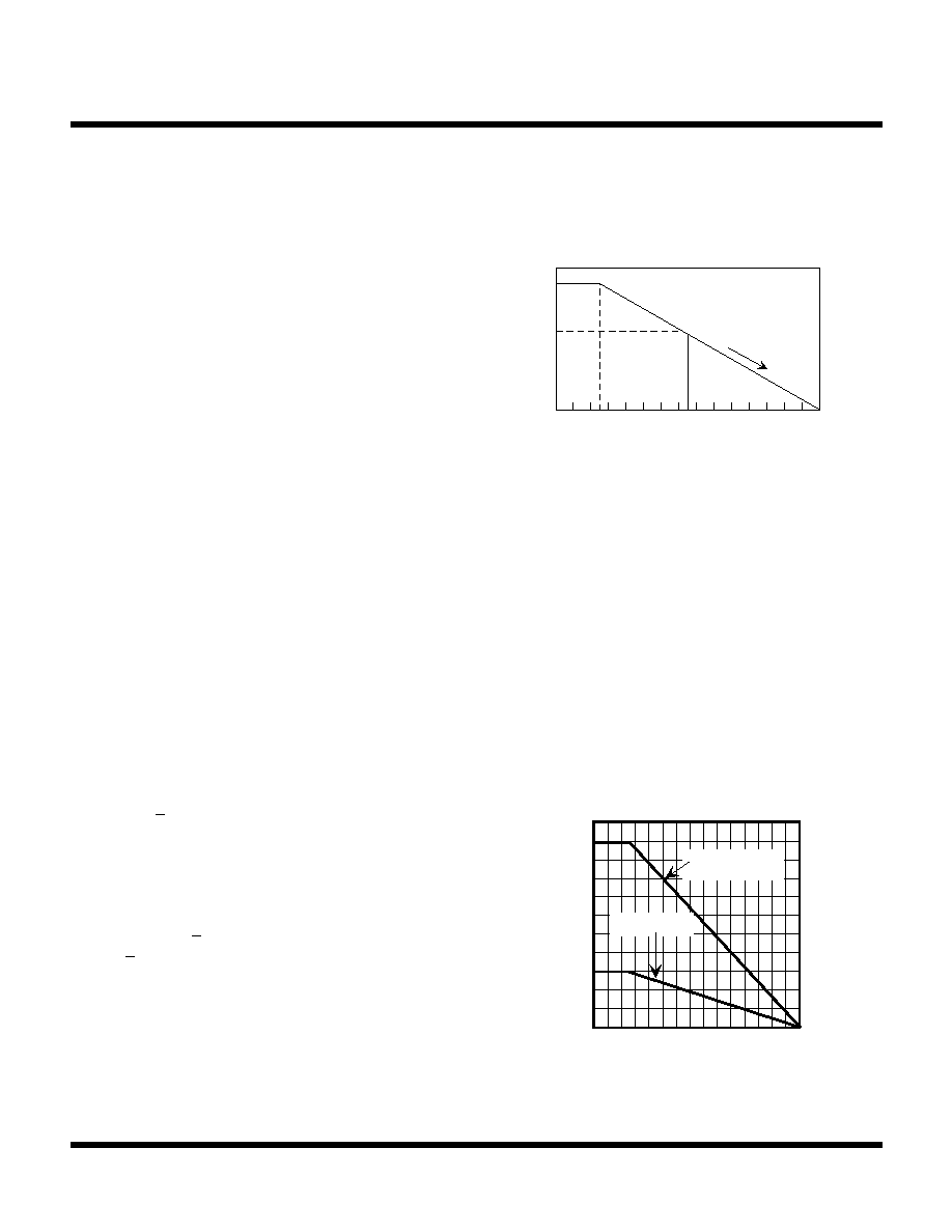
The range of usable currents can also be found from the
graph below.
Procedure:
1) Find P
D
2) P
D1
is taken to be P
D
x (~0.8 - 0.9)
3) Plot P
D1
against 25
∞
C
4) Connect P
D1
to the point corresponding to the 150
∞
C
with a straight line.
5) In design, take a vertical line from the maximum
operating temperature (e.g., 75
∞
C) to the derating
curve.
6) Read off the value of P
D
against the point at which the
vertical line intersects the derating curve. This is taken
as the maximum power dissipation, D
PD
.
The maximum operating current is:
I
OUT
= (D
PD
/ (V
IN(MAX)
-
V
OUT
)
SOT23-5 POWER DISSIPATION CURVE
PD
DPD
25
50
75
150
(mW)
TA (
∞
C)
3
6
5
4
0 50 100 150
TA (
∞
C)
P
D
(
m
W)
0
100
500
MOUNTED AS
SHOWN
FREE AIR
200
300
400
December 1999 TOKO, Inc.
Page 15
TK716xx
INPUT-OUTPUT CAPACITORS
Linear regulators require input and output capacitors in order to maintain regulator loop stability. The equivalent series
resistance (ESR) of the output capacitor must be in the stable operation area. Since the ESR varies widely between
ceramic and tantalum capacitors, the proper IC must be selected according to the output capacitor used:
The TK716xxS is designed for use with ceramic output capacitors.
(Chip tantalum capacitors and electrolytic capacitors with an ESR below 6
can provide stable operation.)
The TK716xxAS is designed for use with tantalum output capacitors.
The DC electrical characteristics and the specifications of the TK716xxS and TK716xxAS are the same; only the value
of the internal phase compensation is different. Increasing the value of the required output capacitor does not cause
abnormal operation. Increasing the value can improve noise reduction, line regulation, load regulation, and stability.
For stable operation, an input capacitor of 0.22
µ
F or more is required.
Note: it is very important to check the selected manufacturers' electrical characteristics. The values of capacitance and
ESR vary from manufacturer to manufacturer, and with product type. A thorough examination is necessary to determine
the characteristics of the capacitor in mass production. The characteristics also vary over temperature. In general, it is
recommended to use as large a value of output capacitance as is practical. Please refer to the following graphs for output
capacitor selection.
APPLICATION INFORMATION
Output side capacitor C
L
= 2.2
µ
F
TK71630S
0 50 100 130
IOUT (mA)
0.1
10
1
100
0.01
Stable area
ESR (
)
TK71630AS
0 50 100 130
IOUT (mA)
0.1
10
1
100
0.01
Stable area
3.3 µF
ESR (
)
Page 16
December 1999 TOKO, Inc.
TK716xx
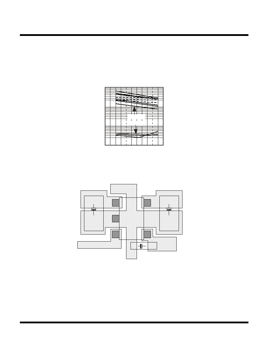
The value of ESR between ceramic and tantalum capacitors differs by about two orders of magnitude as illustrated below.
The characteristics of tantalum capacitors also vary widely according to manufacturer. The output capacitor becomes
a part of the phase compensation in a LDO regulator using a PNP pass transistor. Because of this, it is necessary to
optimize the phase compensation in the IC for use with ceramic or tantalum capacitors.
BOARD LAYOUT
SOT23-5 BOARD LAYOUT
APPLICATION INFORMATION (CONT.)
+
NOISE
BYPASS
CONTROL
VIN
VOUT
+
GND
ESR vs. TEMPERATURE
at 100 kHZ
-20 0 50 60
TEMPERATURE (
∞
C)
0.1
1
10
0.01
ESR (
)
Tantalum Cap
Ceramic Cap

December 1999 TOKO, Inc.
Page 17
TK716xx
REVERSE BIAS PROTECTION
The internal reverse bias protection eliminates the
requirement for a reverse voltage protection diode. This
saves both cost and board space.
Another reverse bias protection technique is illustrated
below. The extra diode and extra capacitor are not
necessary with the TK716xx. The high output voltage
accuracy is maintained because the diode forward voltage
variations over temperature and load current have been
eliminated.
HIGH-SIDE SWITCHING
High-side switching should not be implemented by an
external transistor as shown below. This results in additional
voltage drop and loss of accuracy.
TK716xxS
VOUT
VIN
GND
APPLICATION INFORMATION (CONT.)
The high output voltage accuracy and low dropout voltage
are maintained when the IC is turned ON/OFF by using the
control pin as illustrated below.
High-side switching with a FET is illustrated below. Battery
life is extended by the dropout voltage of the FET when the
input of the TK716xx is connected in front of the FET
switch.
VOLTAGE BACKUP OPERATION (HOLDUP TIME)
C
L
becomes the backup power supply when the
microprocessor is reset with the voltage detector IC
simultaneously with the turning OFF the TK716xx. C
L
provides the holdup time necessary to do an orderly
shutdown of the microprocessor.
TK716xxS
VOUT
VIN
ON/OFF
CONTROL
VOUT
VOLTAGE
REGULATOR
VDROP
TK716xxS
VOUT
VIN
GND
µ PRO
VCONT
VIN
TK716xxS
VOUT
VIN
GND
VOLTAGE
DETECTOR IC
VCONT OFF
µ PRO
RESET
CL
716xx
VOUT
VIN
VCONT
FET SWITCHING OUTPUT
Page 18
December 1999 TOKO, Inc.
TK716xx
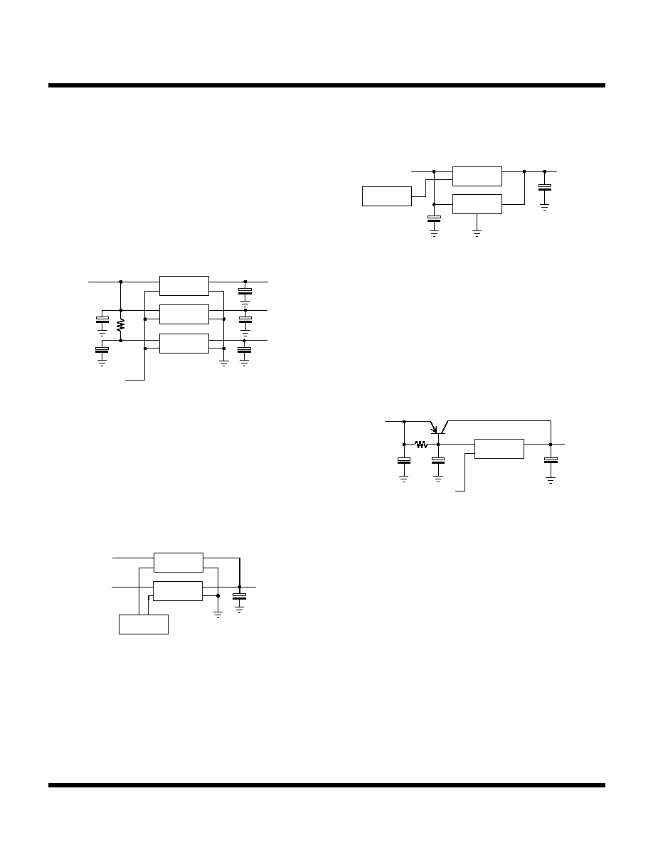
PARALLEL ON/OFF CONTROL
The figure below illustrates multiple regulators being
controlled by a single ON/OFF control signal. The series
resistor R is put in the input line of the low output voltage
regulator in order to prevent overdissipation. The voltage
dropped across the resistor reduces the large input-to-
output voltage across the regulator, reducing the power
dissipation in the device.
SWITCHING OPERATION
Even though the input voltages or the output voltages are
different, the outputs of the TK716xx regulators can be
connected together, and the output voltages switched. If
two or more TK716xx regulators are turned ON
simultaneously, the highest output voltage will be present.
The outputs of the TK716xx regulator and a CMOS regulator
can be connected together as long as the output voltage of
the TK716xx is greater than the CMOS regulator. When
the TK716xx is OFF, the CMOS regulator is turned ON.
When the TK716xx is ON, the CMOS regulator is turned
OFF.
APPLICATION INFORMATION (CONT.)
TK71650
5 V
VIN
TK71630
TK71620
3 V
2 V
ON/OFF CONTROL
R
TK71630
VIN
TK71628
VIN
VOUT
3.0 OR 2.8 V
ON/OFF LOGIC
VCONT
VCONT
CURRENT BOOST OPERATION
The output current can be increased by connecting an
external PNP transistor as shown below. The output
current capability depends upon the H
fe
of the external
transistor. Note: The TK716xx internal short circuit
protection and thermal sensor do not protect the external
transistor.
TK716xx
VIN
CMOS
REGULATOR
VOUT
ON/OFF LOGIC
TK716xx
VIN
VOUT
VCONT
0.22 µF
150
VIN

December 1999 TOKO, Inc.
Page 19
TK716xx
NOTES

Page 20
December 1999 TOKO, Inc.
TK716xx
0.95
0.95
0.95
0.95
e
M
0.1
2.9
1.6
1.1
0.15
0.4
2.8
1.90
2.4
e'
Recommended Mount Pad
1
2
3
4
5
1.0
0.7
(0.8)
0 - 0.1
(0.6)
(0.6)
1.4 max
e
e
e
0.1
e1
0 - 15 max
Marking
±
0.3
+0.15
- 0.05
Dimensions are shown in millimeters
Tolerance: x.x =
±
0.2 mm (unless otherwise specified)
+0.15
-0.05
Marking Information
Part Number TK716xxS TK716xxAS
Marking Marking
TK71613
L13
13L
TK71614
L14
14L
TK71615
L15
15L
TK71616
L16
16L
TK71617
L17
17L
TK71618
L18
18L
TK71619
L19
19L
TK71620
L20
20L
TK71621
L21
21L
TK71622
L22
22L
TK71623
L23
23L
TK71624
L24
24L
TK71625
L25
25L
TK71626
L26
26L
TK71627
L27
27L
TK71628
L28
28L
TK71629
L29
29L
TK71630
L30
30L
TK71631
L31
31L
TK71632
L32
32L
TK71633
L33
33L
TK71634
L34
34L
TK71635
L35
35L
TK71636
L36
36L
TK71637
L37
37L
TK71638
L38
38L
TK71639
L39
39L
TK71640
L40
40L
TK71641
L41
41L
TK71642
L42
42L
TK71643
L43
43L
TK71644
L44
44L
TK71645
L45
45L
TK71646
L46
46L
TK71647
L47
47L
TK71648
L48
48L
TK71649
L49
49L
TK71650
L50
50L
TK71651
L51
51L
TK71652
L52
52L
TK71653
L53
53L
TK71654
L54
54L
Check Table 4 for availability.
SOT23-5
PACKAGE OUTLINE
Printed in the USA
© 1999 Toko, Inc.
All Rights Reserved
TOKO AMERICA REGIONAL OFFICES
Toko America, Inc. Headquarters
1250 Feehanville Drive, Mount Prospect, Illinois 60056
Tel: (847) 297-0070 Fax: (847) 699-7864
IC-216-TK716xx
0798O0.0K
Visit our Internet site at http://www.tokoam.com
The information furnished by TOKO, Inc. is believed to be accurate and reliable. However, TOKO reserves the right to make changes or improvements in the design, specification or manufacture of its
products without further notice. TOKO does not assume any liability arising from the application or use of any product or circuit described herein, nor for any infringements of patents or other rights of
third parties which may result from the use of its products. No license is granted by implication or otherwise under any patent or patent rights of TOKO, Inc.
Western Regional Office
Toko America, Inc.
2480 North First Street , Suite 260
San Jose, CA 95131
Tel: (408) 432-8281
Fax: (408) 943-9790
Midwest Regional Office
Toko America, Inc.
1250 Feehanville Drive
Mount Prospect, IL 60056
Tel: (847) 297-0070
Fax: (847) 699-7864
Eastern Regional Office
Toko America, Inc.
107 Mill Plain Road
Danbury, CT 06811
Tel: (203) 748-6871
Fax: (203) 797-1223
Semiconductor Technical Support
Toko Design Center
4755 Forge Road
Colorado Springs, CO 80907
Tel: (719) 528-2200
Fax: (719) 528-2375