Low Frequency PWM Controlled, StepUp DC/DC Converters
Series
465
4
General Description
Features
Applications
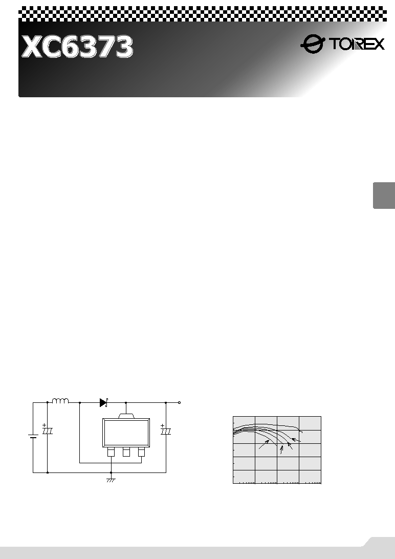
Typical Application Circuit
Typical Performance
Characteristic
The XC6373 is a group of PWM controlled step-up DC/DC converter ICs.
The XC6373 series employs CMOS process and laser trimming
technologies so as to attain low power and high accuracy.
The implemention of a new phase compensation circuit and a slow start
function ensure excellent transient response and improved performance.
The series is particularly suited for use with pager applications because
of their low power consumption and low noise characteristics.
Output voltage can be selected from 2.0V to 7.0V in 0.1V increments
(accuracy; ±2.5%). Oscillator frequency is set at 30kHZ (±20%) so as to
attain the lowest consumption current possible.
A step-up converter circuit can be configured using the XC6373 IC with a
coil, a diode, and a capacitor.
5-pin packages, which are provided with either a CE (Chip enable)
function that reduces power consumption during shut-down mode, or a
V
DD
pin (separated power and voltage detect pins) are available.
SOT-89 small package.
Operating (start-up) voltage range
: 0.9V~10V
Output voltage range : 2.0V~7.0V in 0.1V increments
Highly accurate
: Set-up voltage ±2.5%
Oscillator frequency
: 30kHz (±20%)
Maximum output current (Tr. Built-In)
: 50mA (TYP.) @ V
IN
=3.0V,
V
OUT
=5.0V ....Note (1)
Highly efficient (Tr. Built-In)
: 82% (TYP.) @ V
IN
=3.0V,
V
OUT
=5.0V ....Note (1)
Either chip enable or independent V
OUT
pin option is
selectable for 5-pin package units.
Phase compensation and slow start-up circuits included.
Small Package
: SOT-89 mini-power mold (3-pin, 5-pin)
Note (1): Performance depends on external components and
PCB layout.
GCellular phones, pagers
GPalmtops
GCameras, video recorders
GPortable equipment
NCMOS Low Power Consumption
NOperating Voltage
: 0.9V~10.0V
NOutput Voltage Range
: 2.0V~7.0V
NOutput Voltage Accuracy: ±2.5%
NOscillator Frequency
: 30kHz
0
20
40
60
80
100
0.1
1
10
100
1000
V
IN
=0.9V
1.5V
2.7V
XC6373A300PR
1.2V
1.8V
L100HC54
C
L
47FTantalum
Output Current:I
OUT
mA
Efficiency:EFFI (%)
1
2
3
SOT-89
(TOP VIEW)
V
OUT
GND
C
L
Tantalum
SD
L
C
IN
V
IN
04S_06XC6373 02.09.12 14:49 465
XC6373
Series
466
4
Pin Configulation
Pin Assignment
Product Classification
GSelection Guide
GOrdering Information
q
w
e
Output Voltage
(e.g.,V
OUT
=3.5V
w=3, e=5)
Embossed tape: Standard Feed
Embossed tape: Reverse Feed
OSC Frequency
30kHz
3-pin.
Built-in switching transistor
Stand-by capability.
Built-in switching transistor
Separated V
DD
and V
OUT
Built-in switching transistor
r
t
y
E
C
A
O
P
L
R
XC6373 Series PWM Controlled
XC6373qwerty
Package q=A
SOT-89
q=C,E
SOT-89-5
SOT-89
(TOP VIEW)
1
2
3
SOT-89-5
(TOP VIEW)
1
2
3
4
5
FUNCTION
1
V
SS
Ground
Output voltage monitor,
IC internal power supply
Switch
2
V
OUT
3
L
X
(XC6373A)
PIN NAME
PIN NAME
PIN NUMBER
PIN NUMBER
FUNCTION
5
V
SS
Ground
Output voltage monitor,
IC internal power supply
No connection
2
V
OUT
1
NC
Chip enable
3
CE
Switch
4
L
X
(XC6373C)
PIN NAME
PIN NUMBER
FUNCTION
5
V
SS
Ground
No connection
1
NC
Output voltage monitor
3
V
OUT
Switch
4
L
X
IC internal power supply
2
V
DD
(XC6373E)
PART TYPE
PACKAGE
FEATURES
OPERATION
MODE
SWITCHING
ADDITIONAL
FUNCTION
XC6373A
SOT-89
Switching transistor incorporated standard type.
Low ripple and highly efficient from low current
to high current.
Built-in Transistor
"Lx" lead
XC6373C
SOT-89-5
Stand-by (CE) capability added version to the
XC6373A. Stand-by current; 0.50
µA max.
Built-in Transistor
"Lx" lead
XC6373E
SOT-89-5
Individual power supply and set-up voltage sensing
leads are available.
Built-in Transistor
"Lx" lead
Chip Enable(CE)
Function
Separated
"V
DD
" and "V
OUT
"
PWM
PWM
PWM
04S_06XC6373 02.09.12 14:49 466
XC6373
Series
467
4
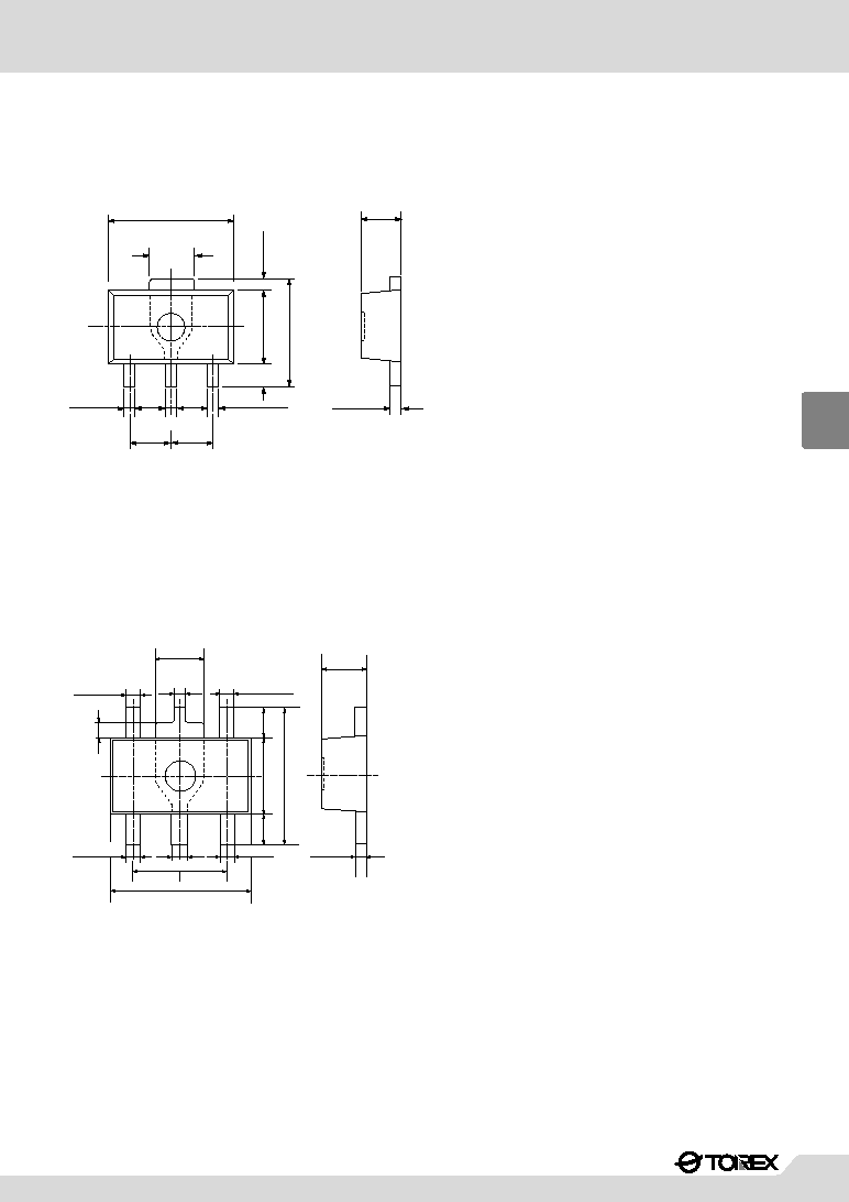
Packaging Information
GSOT-89
GSOT-89-5
4.5±0.1
0.4
2.5±0.1
0.8
min
4.25max
0.42±0.06
0.4
1.5±0.1
0.47±0.06
1.5±0.1
0.42±0.06
1.5±0.1
1.6
+0.15
-0.2
+0.03
-0.02
0.42±0.06
0.42±0.06
0.42±0.06
1.5±0.1
0.8min
0.8min
4.5max
2.5±0.1
0.4
0.42±0.06
0.4
0.42±0.06
0.47±0.06
4.5±0.1
1.5±0.1 1.5±0.1
+0.03
-0.02
1.6
+0.15
-0.2
04S_06XC6373 02.09.12 14:49 467
XC6373
Series
468
4
Marking
SOT-89
(TOP VIEW)
q
w
e
r
2
1
4
3
SOT-89-5
(TOP VIEW)
q Represents the Product Classification
FUNCTION
A
w Represents the integer of the Output Voltage and Oscillator Frequency
1.X
30
kHz
XC63730P
INTEGER OF THE
OUTPUT VOLTAGE
B
5.X
4.X
3.X
2.X
r Denotes the production lot number
0 to 9, A to Z repeated(G.I.J.O.Q.W excepted)
DESIGNATOR
C
D
E
F
6.X
H
7.X
K
-
e Represents the decimal number of the Output Voltage and Oscillator Frequency
X.0
X.9
30
kHz
XC63730P
THE DECIMAL NUMBER
OF OUTPUT VOLTAGE
X.8
X.7
X.6
X.1
X.5
X.4
X.3
X.2
0
9
8
7
6
1
5
4
3
2
PRODUCT NAME
XC6373AP
Built-in Transistor
A
CE
XC6373CP
Built-in Transistor
S
Separated V
DD and
V
OUT
XC6373EP
Built-in Transistor
OSCILLATOR FREQUENCYPRODUCT NAME
OSCILLATOR FREQUENCYPRODUCT NAME
04S_06XC6373 02.09.12 14:49 468

XC6373
Series
469
4
Block Diagram
Buffer
Vref
Soft Start
Phase comp.
Chip Enable
PWM Control
OSC 30KHz
V
DD
CE
-
Note: The CE pin is only used with the XC6373C.
V
SS
Lx
V
OUT
Buffer
Vref
Soft Start
Phase comp.
PWM Control
OSC 30KHz
V
DD
-
Note: The V
DD
pin is only used with the XC6373E.
Lx
V
SS
V
OUT
V
DD
Absolute Maximum Ratings
PARAMETER
Storage Temperature
V
OUT
Input Voltage
L
X
Pin Voltage
L
X
Pin Current
SYMBOL
Tstg
V
OUT
VL
X
IL
X
CONDITIONS
≠40 ~ +125
12
12
400
UNIT
∞C
Operating Ambient
temperature
Topr
≠30 ~ +80
∞C
Continuous Total
Power Dissipation
Pd
500
mW
V
V
mA
Ta=25
∞C
04S_06XC6373 02.09.12 14:49 469

XC6373
Series
470
4
XC6373A330PR
Ta=25
∞C
V
OUT
=3.3V, F
OSC
=30kHz
PARAMETER
Output Voltage
Maximum Input Voltage
SYMBOL
V
OUT
V
IN
CONDITIONS
Operation Start-up Voltage
V
ST
1
External Components Connected.
I
OUT
=1mA.
Oscillation Start-up Voltage
V
ST
2
No external components.
Apply voltage to V
OUT
.
L
X
10k
pull-up to 5V.
Supply Current 1
I
DD
1
Same as V
ST
2.
Apply output voltage
0.95 to V
OUT.
Same as V
ST
2.
Apply output voltage
1.1 to V
OUT
.
Supply Current 2
I
DD
2
L
X
Switch-On Resistance
R
SWON
Same as I
DD
1. VL
X
=0.4V.
L
X
Leak Current
I
LXL
No external components.
V
OUT
=VL
X
=10V.
Oscillator Frequency
F
OSC
Same as I
DD
1.
Measuring of Lx waveform.
Maximum Duty Ratio
MAXDTY
Same as I
DD
1.
Measuring of Lx waveform.
Slow-Start Time
T
SS
MIN
3.128
10
0.80
24
80
TYP
3.300
14.1
4.0
3.4
30
87
10.0
4.0
20.0
MAX
3.383
0.90
23.5
8.1
5.7
1.0
36
92
UNIT
V
V
V
µA
µA
µA
kHz
%
mS
Efficiency
EFFI
77
%
V
Measuring conditions: Unless otherwise specified, V
IN
=V
OUT
0.6, I
OUT
=16.5mA. See Typical Application Circuits, Fig.1.
XC6373A300PR
Ta=25
∞C
V
OUT
=3.0V, F
OSC
=30kHz
PARAMETER
Output Voltage
Maximum Input Voltage
SYMBOL
V
OUT
V
IN
CONDITIONS
Operation Start-up Voltage
V
ST
1
External Components Connected.
I
OUT
=1mA.
Oscillation Start-up Voltage
V
ST
2
No external components.
Apply voltage to V
OUT
.
L
X
:10k
pull-up to 5V.
Supply Current 1
I
DD
1
Same as V
ST
2.
Apply output voltage
0.95 to V
OUT.
Same as V
ST
2.
Apply output voltage
1.1 to V
OUT
.
Supply Current 2
I
DD
2
L
X
Switch-On Resistance
R
SWON
Same as I
DD
1. VL
X
=0.4V.
L
X
Leak Current
I
LXL
No external components.
V
OUT
=VL
X
=10V.
Oscillator Frequency
F
OSC
Same as I
DD
1.
Measuring of Lx waveform.
Maximum Duty Ratio
MAXDTY
Same as I
DD
1.
Measuring of Lx waveform.
Slow-Start Time
T
SS
MIN
2.925
10
0.80
24
80
TYP
3.000
13.1
3.9
3.4
30
87
10.0
4.0
20.0
MAX
3.075
0.90
21.9
7.9
5.7
1.0
36
92
UNIT
V
V
V
µA
µA
µA
kHz
%
mS
Efficiency
EFFI
77
%
V
Measuring conditions: Unless otherwise specified, V
IN
=V
OUT
0.6,I
OUT
=15mA. See Typical Application Circuits, Fig.1.
Electrical Characteristics
04S_06XC6373 02.09.12 14:49 470
XC6373
Series
471
4
1
2
3
5
4
(TOP VIEW)
SOT-89-5
1
2
3
SOT-89
(TOP VIEW)
V
OUT
V
OUT
CE
1
2
3
5
4
(TOP VIEW)
SOT-89-5
V
DD
V
OUT
GND
GND
GND
C
L
Tantalum
C
L
Tantalum
C
L
Tantalum
SD
SD
SD
V
IN
V
IN
L
L
L
C
IN
C
IN
C
IN
V
IN
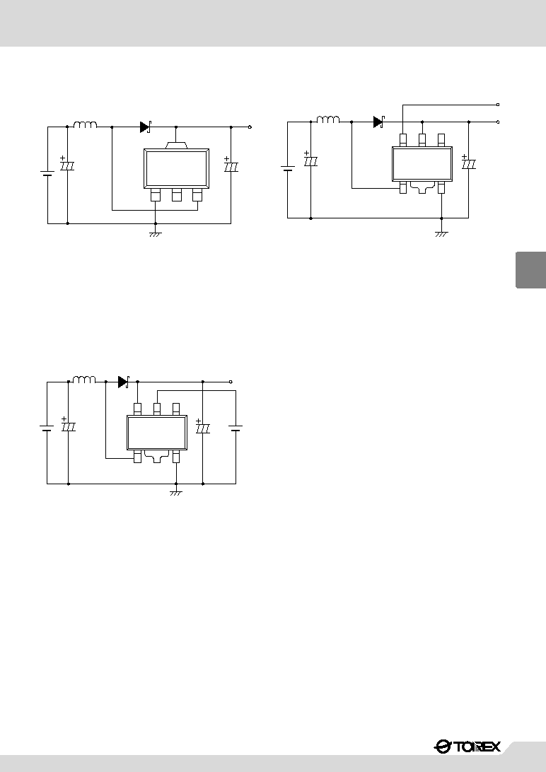
Fig.3 XC6373C Application
L
: 100
µH (SUMIDA, CR-54)
SD : MA2Q735 (Schottky diode; MATSUSHITA)
C
L
: 16V 47
µF (Tantalum capacitor; NICHICON, MCE)
C
IN
: 16V220
µF (Aluminium Electrolytic Capacitor)
Fig.1 XC6373A Application
L
: 100
µH (SUMIDA, CR-54)
SD : MA2Q735 (Schottky diode; MATSUSHITA)
C
L
: 16V 47
µF (Tantalum capacitor; NICHICON, MCE)
C
IN
: 16V220
µF (Aluminium Electrolytic Capacitor)
Fig.5 XC6373E Application
L
: 100
µH (SUMIDA, CR-54)
SD : MA2Q735 (Schottky diode; MATSUSHITA)
C
L
: 16V 47
µF (Tantalum capacitor; NICHICON, MCE)
C
IN
: 16V220
µF (Aluminium Electrolytic Capacitor)
Typical Application Circuits
04S_06XC6373 02.09.12 14:49 471
XC6373
Series
472
4
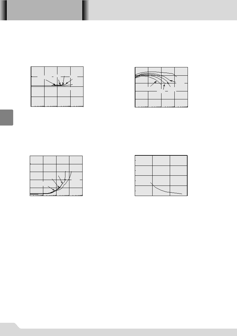
2.90
2.95
3.00
3.05
3.10
0.1
1
10
100
1000
XC6373A300PR
L=100H(C54),C
L
=47F()
1.5V
1.2V
1.8V
2.7V
V
IN
=0.9V
Output Current: I
OUT
(mA)
Output Voltage: V
OUT
( V
)
L100H, C
L
47FTantalum
0
20
40
60
80
100
0.1
1
10
100
1000
1.5V
XC6373A300PR
1.2V
1.8V
2.7V
L100H, C
L
47FTantalum
V
IN
=0.9V
Output Current: I
OUT
(mA)
Efficiency: EFFI (%)
0
20
40
60
80
100
0.1
1
10
100
1000
1.5V
XC6373A300PR
1.2V
1.8V
2.7V
L100H, C
L
47FTantalum
Output Current: I
OUT
(mA)
V
IN
=0.9V
Ripple Voltage: Vr (mVp-p)
200
150
100
50
0
0
1
2
3
XC6373A300PR
L100H, C
L
47FTantalum
Input Voltage: V
IN
(V)
Intput Current: I
IN
(
µ
A)
Typical Performance Characteristics
(1) OUTPUT VOLTAGE vs. OUTPUT CURRENT
Topr=25∞C
(2) EFFICIENCY vs. OUTPUT CURRENT
Topr=25∞C
(3) RIPPLE VOLTAGE vs. OUTPUT CURRENT
Topr=25∞C
(4) NO LOAD INPUT CURRENT vs. INPUT VOLTAGE
Topr=25∞C
04S_06XC6373 02.09.12 14:49 472