
ICs for use with 3rd Overtone Crystal Oscillators
Series
1031
14
The XC2163 series are high frequency, low current consumption CMOS
ICs with built-in crystal oscillator and divider circuits.
Output is selectable from any one of the following values for f0 :
f0/1, f0/2, f0/4, f0/8.
With oscillation capacitors and a feedback resistors built-in, it is possible
to configure a stable 3rd overtone oscillator using only an external crystal
oscillator.
Also available is an external oscillation capacitor/external oscillation
feedback resistor type which makes oscillation frequency control
possible.
General Description
Oscillation Frequency
: 40MHz ~ 125MHz (Rf, Cg, Cd
internal ; 5.0V)
(3rd Overtone)
: 57MHz ~ 125MHz (Rf, Cg, Cd
internal ; 3.3V)
: 20MHz ~ 125MHz (Rf, Cg, Cd
external)
Divider Ratio
: Selectable from f0/1, f0/2, f0/4,
f0/8.
Output
: 3-State
Operating Voltage Range : 3.3V �10%, 5.0V �10%
Low Current Consumption : Stand-by function included *
Ultra Small Package
: SOT-26 mini mold
* oscillation continues in stand-by mode
GCrystal Oscillation Modules
GComputer, DSP Clocks
GCommunication Equipment
GVarious System Clocks
Features
Applications
NCMOS
NOscillation Frequency : 125MHz (max)
N3-State Output
NBuilt-in Oscillation Capacitor
NBuilt-in Oscillation Feedback Resistor
NMini Mold SOT-26 Package
/INH
"H"
"L"
OPEN
"H" = High Level
"L" = Low Level
Divider Output
Q
0
Divider Output
High Impedance
SOT-26
( TOP VIEW )
1
/INH
XT
/XT
PIN
NUMBER
PIN NAME
1
/INH
2
XT
3
4
Qo
5
6
/XT
Power Supply
Crystal Oscillator Connection (Output)
GND
FUNCTION
Crystal Oscillator Connection (Input)
Stand-by control*
Clock Output
V
SS
V
DD
* Stand-by control pin has pull-up resistance built-in.
V
SS
Q
O
V
DD
Pin Configuration
Pin Assignment
/INH, Q0 Pin Function
14S_04XC2163 02.09.12 16:36 1031

XC2163
Series
1032
14
XC2163
qwerty
Table 1: Frequency for External Type
Frequency Range
Frequency Range
SYMBOL
5.0V TYPE
3.3V TYPE
DESIGNATOR
DESCRIPTION
DESIGNATOR
DESCRIPTION
Note : We recommend that a damping resistor Rd be added between the /XT pin & the crystal oscillator pin in order to safeguard
the crystal oscillator and improve oscillation stability.
/
/
Output Capacity :
5 = 10TTL
Duty Level :
1 = CMOS (V
DD
/2)
Note :
TTL : 20MHz to 37MHz
C = f0/1
E = f0/4
D = f0/2
F = f0/8
Ratio Divider :
Recommended Frequency Range
& Rf, Cg, Cd values
External Type:Z(refer to table 1)
Built-in Type:(To Be Determined)
Package :
M = SOT-26
Device Orientation :
R = Embossed Tape
(Standerd Feed)
L= Embossed Tape
(Reverse Feed)
Product Classification
GOrdering Information
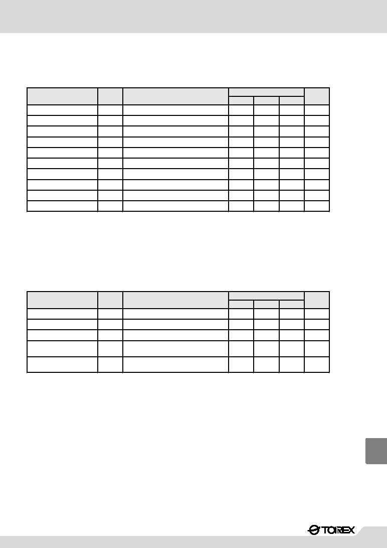
Table 2: Frequency for Internal Type
Frequency Range
Frequency Range
SYMBOL
5.0V TYPE
3.3V TYPE
/
/
A
-
-
-
108MHz 125MHz
1.5k
5.5pF
B
-
-
-
93MHz 110MHz
1.7k
6.5pF
C
108MHz 125MHz
2.2K
5.5pF
80MHz 95MHz
2.2k
5.5pF
D
95MHz 110MHz
2.4K
6.5pF
72MHz 83MHz
2.4k
6.5pF
E
80MHz 97MHz
3.2K
6.5pF
65MHz 75MHz
3.2k
6.5pF
F
68MHz 83MHz
3.7K
6.5pF
57MHz 67MHz
3.7k
6.5pF
H
55MHz 70MHz
4.9K
7.6pF
-
-
-
K
45MHz 57MHz
5.5K
11pF
-
-
-
L
40MHz 48MHz
6.5K
11pF
-
-
-
14S_04XC2163 02.09.12 16:36 1032

XC2163
Series
1033
14
q
w
MARK
RATIO
MARK
RATIO
MARK
MARK
Frequency (MHz)
A
B
C
D
E
F
H
K
L
Z
�
�
108~125
95~110
80~97
68~83
55~70
45~57
40~48
108~125
93~110
80~95
72~83
65~75
57~67
�
�
�
6
e
r
1
q w e r
SOT-26
(TOP VIEW)
Represents Frequency & Rf,
Cg & Cd Values
Represents the Assembly Lot No.
(based on internal standards)
/
/
/
/
Represents the Series name
Represents the Divider Ratio
External
5.0V
3.3V
Marking
Absolute Maximum Ratings
Block Diagram
Rup
Cg
Cd
Rf
1/2
1/2
1/2
XT
/XT
/INH
Rup
1/2
1/2
1/2
XT
/XT
/INH
V
DD
V
DD
Q
O
Q
O
V
SS
V
SS
q Built -in oscillation capacitors, oscillation feedback resistor
w External oscillation capacitors, oscillation feedback resistor
PARAMETER
SYMBOL
CONDITIONS
UNITS
Supply Voltage
V
Input Voltage
V
Continuous Total
Power Dissipation
Pd
mW
Operating Ambient
Temp.
Topr
Storage Temp.
Tstg
V
SS
-0.3V
SS
+7.0
V
SS
-0.3V
DD
+0.3
250 *
-30+80
-55+125
V
DD
V
IN
* when implemented on a glass epoxy PCB
Packaging Information
GSOT-26
0.95
0.5
1.9�0.2
2.9�0.2
1.1�0.1
00.1
0.15
0.2min
+0.1
-0.05
0.4
+0.1
-0.05
2.8�0.2
1.6
+0.2
-0.1
0.4
+0.1
-0.05
14S_04XC2163 02.09.12 16:36 1033

XC2163
Series
1034
14
Electrical Characteristics
MIN
TYP
MAX
tr
tf
1.5
1.5
DUTY
45
55
PARAMETER
SYMBOL
CONDITIONS
tplz
100
Output Rise Time
Output Fall Time
Output DUTY Cycle
Output Disable
(Delay Time)
C
L
=15pF, 0.1V
DD
0.9V
DD
C
L
=15pF, 0.9V
DD
0.1V
DD
C51A 0.5V
DD
, C
L
=15pF, f=125MHz
C51B 0.5V
DD
, C
L
=15pF, f=110MHz
C
L
=15pF
Standard value
MIN
TYP
MAX
Operating Voltage
2.97
3.63
V
/INH pin
2.4
V
/INH pin
0.4
V
2.2
2.4
V
0.3
0.4
V
Consumption Current 1
18
mA
Consumption Current 2
/INH = 'L', f = 125MHz
5
A
/INH = 'L'
1.0
2.0
4.0
M
35
70
140
k
5.5
pF
PARAMETER
SYMBOL
CONDITIONS
UNITS
XC2163C51AMR/XC2163C51BMR
CMOS DUTY: V
DD
=3.3V, Ta=25
fosc=108MHz125MHz
XC2163C51AMR:
Unless specified, V
DD
=3.3V, Ta=25
Qo pin, V
DD
= 2.97V, I
OH
= -8mA
Qo pin, V
DD
= 2.97V, I
OL
= 8mA
/INH = OPEN, C
L
= 15pF, f = 125MHz
/INH = 0.7V
DD
Measured Value
'H' Level Input Voltage
'L' Level Input Voltage
'H' Level Output Voltage
'L' Level Output Voltage
Input pull up resistance 1
Input pull up resistance 2
Internal oscillation capacity
V
DD
V
IH
V
IL
V
OH
V
OL
I
DD
1
I
DD
2
Rup1
Rup2
Cg
Measured Value
5.5
pF
1.5
M
10
A
note) measured value
Qo pin, /INH = 'L'
/INH pin
/INH pin
/INH = 'L', f = 110MHz
/INH = 'L'
Qo pin, V
DD
= 2.97V, I
OH
= -8mA
Qo pin, V
DD
= 2.97V, I
OL
= 8mA
/INH = OPEN, C
L
= 15pF, f = 110MHz
/INH = 0.7V
DD
Measured Value
Measured Value
Qo pin, /INH = 'L'
Internal oscillation feedback resistance
Output Off Leak Current
Operating Voltage
Consumption Current 1
Consumption Current 2
'H' Level Input Voltage
'L' Level Input Voltage
'H' Level Output Voltage
'L' Level Output Voltage
Input pull up resistance 1
Input pull up resistance 2
Internal oscillation capacity
Internal oscillation feedback resistance
Output Off Leak Current
Cd
Rf
I
OZ
Standard value
MIN
TYP
MAX
2.97
3.63
V
2.4
V
0.4
V
2.2
2.4
V
0.3
0.4
V
15
mA
5
A
1.0
2.0
4.0
M
35
70
140
k
6.5
pF
PARAMETER
SYMBOL
CONDITIONS
UNITS
V
DD
V
IH
V
IL
V
OH
V
OL
I
DD
1
I
DD
2
Rup1
Rup2
Cg
6.5
pF
1.7
M
10
A
Cd
Rf
I
OZ
fosc=93MHz110MHz
XC2163C51BMR:
Unless specified, V
DD
=3.3V, No load, Ta=25
Switching Characteristics
14S_04XC2163 02.09.12 16:36 1034
Standard value
MIN
TYP
MAX
Operating Voltage
4.5
5.5
V
/INH pin
2.4
V
/INH pin
0.4
V
3.9
4.2
V
0.3
0.4
V
Consumption Current 1
31
mA
Consumption Current 2
/INH = 'L', f = 120MHz
14
mA
/INH = 'L'
0.5
1.0
2.0
M
25
50
100
k
10
A
PARAMETER
SYMBOL
CONDITIONS
UNITS
Standard value
PARAMETER
SYMBOL
CONDITIONS
UNITS
MIN
TYP
MAX
tr
1.5
ns
tf
1.5
ns
DUTY
45
55
%
tplz
100
ns
tpzl
100
ns
CMOS DUTY : V
DD
=5.0V, Ta=25
fosc = 108MHz to 125MHz ; Rf = 1.6k
; Cg = Cd = 10pF external
XC2163C51ZMR:
Unless specified, V
DD
=5.0V, Ta=25
This data sheet is preliminary therefore, the contents can be changed
without advance notice.
Qo pin, V
DD
= 4.5V, I
OH
= -16mA
Qo pin, V
DD
= 4.5V, I
OL
= 16mA
/INH = OPEN, C
L
= 15pF, f = 120MHz
/INH = 0.7V
DD
Qo pin, /INH = 'L'
'H' Level Input Voltage
'L' Level Input Voltage
'H' Level Output Voltage
'L' Level Output Voltage
Input pull up resistance 1
Input pull up resistance 2
Output Off Leak Current
V
DD
V
IH
V
IL
V
OH
V
OL
I
DD
1
I
DD
2
Rup1
Rup2
I
OZ
Output Rise Time
Output Fall Time
Output DUTY Cycle
Output Disable
(Delay Time)
Output Enable
(Delay Time)
C
L
=15pF, 0.1V
DD
0.9V
DD
C
L
=15pF, 0.9V
DD
0.1V
DD
0.5V
DD
, C
L
=15pF, f=120MHz
C
L
=15pF
C
L
=15pF
Electrical Characteristics
Switching Characteristics
XC2163
Series
1035
14
14S_04XC2163 02.09.12 16:36 1035