July 30, 2003 Ver. 5
CMOS Low Power Consumption
APPLICATIONS
Oscillation Frequency 4MHz to 125MHz
Crystal Oscillation Modules
4MHz to 30MHz
(Fundamental Oscillation)
Micro computer, DSP Clocks
20MHz to 125MHz
(3rd Overtone Oscillation)
Communication Equipment
3 State Output
Various System Clocks
Built-in Capacitors Cg, Cd
Built-in Feedback Resistor
Chip form
Mini Mold SOT-26 Package
GENERAL DESCRIPTION
FEATURES
Oscillation Frequency:
4MHz to 30MHz (Fundamental)
20MHz to 125MHz (3rd Overtone)
Divider Ratio:
Selectable from f0/1, f0/2, f0/4, f0/8.
( f0/2, f0/4, f0/8 are fundamental only)
Output:
3-State
Operating Voltage Range: 3.3V ± 10%, 5.0V ± 10%
Low Power Consumption: Stand -by function included
Selectable from C/E type and O/E type
Chip Form:
Chip Size 1.3
◊
0.8 mm
Ultra Small Package:
SOT-26 mini mold
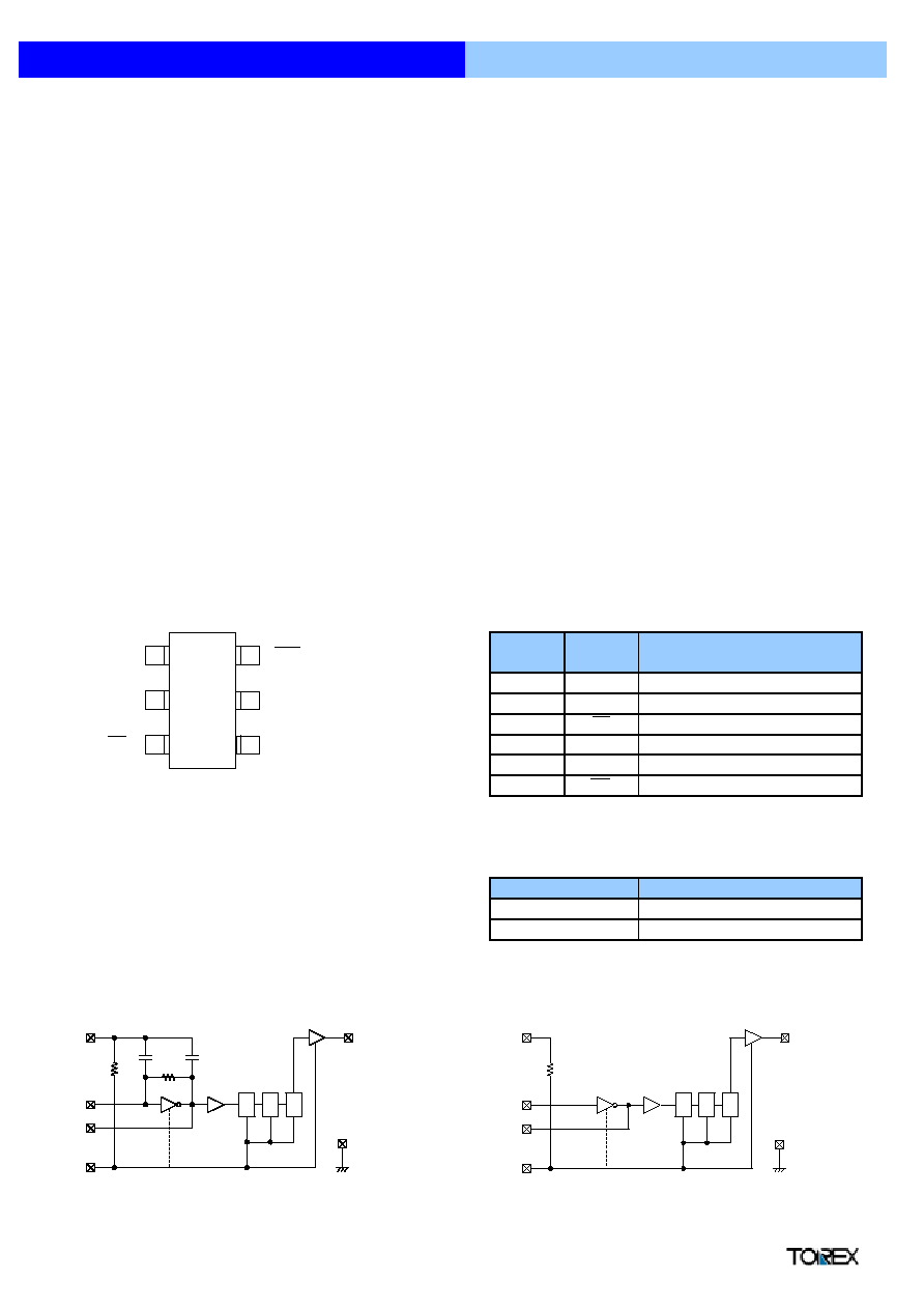
PIN CONFIGURATION
PIN ASSIGNMENT
* Stand-by control pin has a pull-up resistor built-in.
/INH, Q0 PIN FUNCTION
BLOCK DIAGRAM
VDD
Crystal Oscillator Connection (Output)
Crystal Oscillator Connection (Input)
/INH
Q0
"H" or OPEN
Clock Output
Stand-by Control*
4
XT
1
2
Q0
3
VSS
XT
6
INH
5
XC2164 Series
ICs for use with Crystal Oscillators
The XC2164 series are high frequency, low current
consumption CMOS ICs with built-in crystal oscillator and
divider circuits.
For fundamental oscillation, output is selectable from any one
of the following values for f0 : f0/1, f0/2, f0/4, f0/8.
With oscillation capacitors and a feedback resistor built-in, it
is possible to configure a stable fundamental oscillator or 3rd
overtone oscillator using only an external crystal.
Also available is an external oscillation capacitor / external
oscillation feedback resistor type which makes oscillation
frequency control possible.
The XC2164 series are integrated into SOT-26 packages.
The series is also available in chip form.
SOT-26 (TOP VIEW)
PIN NUMBER
PIN NAME
FUNCTION
Power Supply
Clock Output
Ground
"L"
High Impedance
1
2
4
3
5
6
Q0
V
SS
XT
INH
V
DD
XT
Rup
Cg
Cd
Rf
1/2
1/2
1/2
V
DD
XT
/XT
/INH
Q
O
V
SS
Rup
1/2
1/2
1/2
V
DD
XT
/XT
/INH
Q
O
V
SS
Built-in oscillation capacitors, oscillation feedback resistor
External oscillation capacitors, oscillation feedback resistor
Semiconductor Ltd.
1
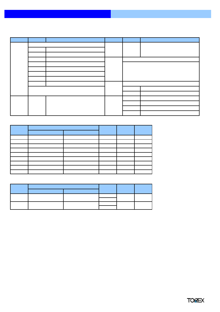
ORDERING INFORMATION
XC2164
123456
Duty Level
f0/1
Chip Enable
CMOS (VDD/2)
f0/2
Chip Enable
Note : TTL : Fundamental 4MHz to 30MHz
f0/4
Chip Enable
f0/8
Chip Enable
Built-in Type
(3rd O/T)
=refer to table 1
f0/1
Output Enable
Built-in Type
(Fundamental)
=refer to table 2
f0/2
Output Enable
f0/4
Output Enable
f0/8
Output Enable
Note : f0/2, f0/4, f0/8 are fundamental only
Chip Form
SOT-26
Embossed Tape: Standard Feed
Embossed Tape: Reverse Feed
Chip Tray
Wafer
Table 1: Built-in Type (3rd O/T)
Table 2 : Built-In Type (Fundamental)
(*) Rf=3.5M
@V
DD
=5.0V Operation
Rf=7.0M
@V
DD
=3.3V Operation
T
4MHz to 30MHz
4MHz to 30MHz
3.5
DESCRIPTION
Ratio Divider & Stand-By Mode
2
5
Fixed Number
1
B
K
L
A
C
M
5
5.5
(pF)
Cd
14.0
9.0
5.0
16.0
Cg
Package
Rf
Cg
Cd
(k
)
(pF)
12.5
12.5
3.5
2.0
7.0
L
110MHz to 125MHz
3.3V ± 10%
40MHz to 50MHz
Frequency Range
30MHz to 40MHz
-
20MHz to 30MHz
30MHz to 40MHz
A
B
C
95MHz to 110MHz
40MHz to 50MHz
50MHz to 65MHz
65MHz to 80MHz
80MHz to 95MHz
35.0
4MHz to 30MHz
4MHz to 30MHz
3.5
7.0
35.0
SYMBOL
SYMBOL
5.0V ± 10%
E
F
H
K
4
SYMBOL
3
1
Recommended Frequency Range & Rf, Cg, Cd values
N
W
L
21.5
21.5
6
R
5.0V ± 10%
20MHz to 30MHz
(pF)
50MHz to 65MHz
65MHz to 80MHz
20.0
DESIGNATOR
D
6.5
20.0
SYMBOL
DESIGNATOR
DESCRIPTION
3.3V ± 10%
Rf (*)
(M
)
2.3
D
(pF)
Frequency Range
M, V
80MHz to 95MHz
95MHz to 110MHz
2.8
110MHz to 125MHz
-
C
T
M
7.0
5.5
2.5
2.2
16.0
10.0
10.0
8.0
8.0
20.0
7.0
20.0
14.0
XC2164 Series
ICs for use with Crystal Oscillators
Semiconductor Ltd.
2

PACKAGING INFORMATION
SOT-26
PAD LAYOUT
PAD DIMENSIONS
unit [
µ
m]
Chip Size
1.3
◊
0.8 mm
Chip Thickness 280 ± 20
µ
Pad Aperture
100
◊
100
µ
* Stand-by control pin has a pull-up resistor built-in.
MARKING RULE
1
Represents product series : XC2164 series
2
Represents divider ratio
<Chip Enable>
* B,C,D : fundamental only.
<Output Enable>
* L,M,N : fundamental only.
3
Represents recommended frequency & Rf, Cg & Cd values
*) Please refer to the ordering information table above.
4
Represents the assembly lot no.
(Based on internal standards.)
RATIO
RATIO
K
L
RATIO
f0/1
f0/2
M
N
RATIO
MARK
A
B
MARK
C
D
f0/4
f0/8
f0/4
f0/8
XC2164 Series
f0/1
f0/2
FUNCTION
Q0
Clock Output
SOT-26 (TOP-VIEW)
PIN NAME
1
514
27
-264
-264
514
222
-450
-264
47
264
-450
264
MARK
MARK
ICs for use with Crystal Oscillators
PIN NUMBER
PAD DIMENSIONS
X
Y
VDD
Power Supply
2
VSS
Ground
6
INH
Stand-by Control*
3
XT
Crystal Oscillator
Connection (Output)
4
XT
Crystal Oscillator
Connection (Input)
5
1
2
3
4
6
5
(650,400)
(-650,-400)
Y
X
6
5
4
3
2
1
1
2
3
4
Semiconductor Ltd.
3

July 30, 2003 Ver. 5
ABSOLUTE MAXIMUM RATINGS
*When implemented on a glass epoxy PCB (SOT26 package)
ELECTRICAL CHARACTERISTICS
XC2164A51M, T, V Fundamental
5.0V Operation (unless otherwise stated, VDD=5.0V, No Load, Ta=30 ~ + 80
O
C)
/INH=Open, Q0=Open
XC2164A51M, V
f=30MHz
XC2164A51T
/INH= " L ", Q0=Open
XC2164A51M, V
f=30MHz
XC2164A51T
XC2164A51M, V
XC2164A51T
XC2164A51M, V
XC2164A51T
note 1 : the values for Cg, Cd are the designed values.
XC2164A51M Fundamental
3.3V Operation (unless otherwise stated, VDD=3.3V, No Load, Ta=30 ~ + 80
O
C)
/INH=Open, Q0=Open
XC2164A51M, V
f=30MHz
XC2164A51T
/INH= " L ", Q0=Open
XC2164A51M, V
f=30MHz
XC2164A51T
XC2164A51M, V
XC2164A51T
XC2164A51M, V
XC2164A51T
* note 1 : the values for Cg, Cd are the designed values.
Cd
( * )
35
20
2
( 4 )
( * )
/INH=0.7VDD
35
2
( 4 )
2.4
MAX.
2.97
µ
A
35
Consumption Current 1
Consumption Current 2
IDD1
IDD2
/INH=0.7VDD
/INH="L"
CMOS : 2.97V, IOH= - 8mA
Output Diable Leakage Current
VIH
Operating Supply Voltage
Internal Oscillation Feedback Resistance
Consumption Current 2
IDD2
Internal Oscillation Capacitance
Cg
Input pull up resistance 2
Consumption Current 1
IDD1
"H" Level Input Voltage
"L" Level Input Voltage
"H" Level Input Voltage
"L" Level Input Voltage
PARAMETER
Internal Oscillation Capacitance
"H" Level Output Voltage
"L" Level Output Voltage
Input pull up resistance 1
Input pull up resistance 2
Rup2
Rup1
CMOS : VDD -= 4.5V, IOH= - 16mA
CMOS : VDD = 4.5V, IOH=16mA
/INH="L"
VIL
XC2164 Series
ICs for use with Crystal Oscillators
UNITS
V
V
TYP.
VIH
2.4
MIN.
4.5
VDD
VOL
Output Disable Leakage Current
Internal Oscillation Feedback Resistance
Cd
Input pull up resistance 1
/INH="L"
Rup2
35
5
4
Rup1
1.0
2.0
70
VOH
2.5
"H" Level Output Voltage
VOL
"L" Level Output Voltage
CMOS : 2.97V, IOH=8mA
VIL
Rf
IOZ
3.30
3.63
SYMBOL
MIN.
TYP.
VDD
CONDITIONS
10
/INH="L"
Rf
25
3.5
20
IOZ
Cg
35
50
( * )
( * )
20
5
0.5
1.0
5
11
VOH
3.9
4.2
0.4
100
11
( 15 )
0.3
( 8 )
2.0
( 8 )
( 15 )
MAX.
5.5
5.0
SYMBOL
PARAMETER
CONDITIONS
Tstg
O
C
-65 ~ +150 (Chip Form)
V
Operating Supply Voltage
SYMBOL
UNITS
CONDITIONS
Vss - 0.3 to Vss + 7.0
VIN
Pd
250*
Vss - 0.3 to VDD + 0.3
VDD
Storage Temperature
Topr
Operating Ambient
Temperature
-55 ~ +125 (SOT-26)
-40 ~ +85
M
µ
A
M
0.4
V
pF
mA
( 6.5 )
4.0
140
µ
A
0.4
V
V
( 8 )
20
7.0
10
PARAMETER
Supply Voltage
Input Voltage
Continuous Total Power
Dissipation
V
V
V
V
O
C
mW
O
C
0.4
mA
M
k
pF
M
µ
A
UNITS
V
V
k
Semiconductor Ltd.
4

ELECTRICAL CHARACTERISTICS (Continued)
XC2164A51T, V Fundamental
3.3V Operation (unless otherwise stated, VDD=3.3V, No Load, Ta=30 ~ + 80
O
C)
/INH=Open, Q0=Open
XC2164A51M, V
f=30MHz
XC2164A51T
/INH= " L ", Q0=Open
XC2164A51M, V
f=30MHz
XC2164A51T
XC2164A51M, V
XC2164A51T
XC2164A51M, V
XC2164A51T
* note 1 : the values for Cg, Cd are the designed values.
Comparative Chart of Oscillation Frequency vs. Supply Voltage, and Negative Resistance Value (The designed value when 300MHz Crystal is used.)
OSCILLATION FREQUENCY vs. SUPPLY VOLTAGE
VDD = 3.3V
VDD = 5.0V
- 130
- 220
- 660
- 760
- 250
3.30
2.5
NEGATIVE RESISTANCE VALUE
±
1.2 ppm
VDD = 5.0 V,
±
10%
VDD = 3.3 V,
±
10%
±
4.3 ppm
±
4.5 ppm
CMOS : 2.97V, IOH= - 8mA
- 150
SYMBOL
±
9.4 ppm
M
V
T
±
2.1 ppm
±
7.0 ppm
Operating Supply Voltage
VDD
2.5
"H" Level Input Voltage
VIH
PARAMETER
SYMBOL
CONDITIONS
MIN.
TYP.
MAX.
UNITS
3.63
V
V
"L" Level Input Voltage
VIL
0.4
V
"H" Level Output Voltage
VOH
2.4
"L" Level Output Voltage
VOL
CMOS : 2.97V, IOH=8mA
( 6.5 )
V
0.4
V
( 8 )
mA
Consumption Current 2
IDD2
2
Consumption Current 1
IDD1
5
4
µ
A
2
( 4 )
( 4 )
Input pull up resistance 1
Rup1
/INH="L"
1.0
2.0
4.0
M
Input pull up resistance 2
Rup2
/INH=0.7VDD
35
70
140
k
Internal Oscillation Capacitance
Cg
( * )
Cd
( * )
35
pF
20
35
Internal Oscillation Feedback Resistance
Rf
10
µ
A
20
7.0
XC2164 Series
ICs for use with Crystal Oscillators
M
Output Diable Leakage Current
IOZ
/INH="L"
Semiconductor Ltd.
5