
ICs for use with Crystal Oscillators (PLL builtin)
Series
1039
14
The XC2173 series are high frequency, low power consumption CMOS
ICs with built-in crystal oscillator, divider and clock multiplier PLL circuits.
Output is selectable from any one of the following values for f0 :
f0 x 5, f0 x 6, f0 x 7, f0 x 8, f0/2, f0/4, f0/8. With an oscillation capacitor &
oscillation feedback resistor built-in, a stable oscillator circuit can be put
together using only an external crystal oscillator.
By connecting an external standard clock, the above mentioned output
frequencies can be achieved.
General Description
Oscillation Frequency
: 10MHz ~ 25MHz
Divider Ratio
: f0/2, f0/4, f0/8
Multiplier
: f0 x 5, f0 x 6, f0 x 7, f0 x 8
Output
: 3-State
Operating Voltage Range
: 3.3V ±10% and 5.0V ±10%
Small Consumption Current : Stand-by function included*
* oscillation continues in stand-by
Ultra Small Package
: SOT-26 mini mold
GCrystal Oscillation Modules
GComputer, DSP Clocks
GCommunication Equipment
GVarious System Clocks
Features
Applications
NCMOS
NOscillation Frequency
: 10MHz ~ 25MHz
NOutput Frequency : 80MHz ~ 160MHz (5.0V)
: 50MHz ~ 125MHz (3.3V)
NDivider Circuit & PLL Circuit Built-In
N3-State Output
NOscillation Capacitor & Oscillation Feedback
Resistor Built-In
NMini Mold SOT-26 Package
Pin Configuration
Pin Assignment
1
/INH
XT
/XT
SOT-26
( TOP VIEW )
PIN
NUMBER
PIN NAME
1
/INH
2
XT
3
4
Qo
5
6
/XT
FUNCTION
Crystal Oscillator Connection (Input)
Power Supply
Crystal Oscillator Connection (Output)
/ Standard Clock Input
GND
* Stand-by control pin has pull-up resistor built-in.
Clock Output
Stand-by control*
V
DD
V
SS
V
DD
Q
O
V
SS
/INH
"H"
"L"
OPEN
"H" = High Level
"L" = Low Level
Divider/Multiplier Output
Q
0
Divider/Multiplier Output
High Impedance (Stand-by)
INH - B, Q0 Pin Function
14S_05XC2173 02.09.12 16:37 1039

XC2173
Series
1040
14
qwerty
DESIGNATOR
DESCRIPTION
DESIGNATOR
DESCRIPTION
Duty Level :
C : CMOSV
DD
/2
Input Oscillation Frequency Range
1 : 10MHz to 25MHz
Package :
M = SOT-26
Multiplier Ratio or Divider Ratio
2 : f0 / 2
6 : f0 x 6
4 : f0 / 4
7 : f0 x 7
5 : f0 x 5
8 : f0 / 8 & f0 x 8
Device Orientation :
R = Embossed Tape
(Standard Feed)
L= Embossed Tape
(Reverse Feed)
Output Capacity :
M : Multiplier Output
D : Divider Output
Product Classification
GOrdering Information
Marking
q Represents the Series name
w Represents the Output
SYMBOL
OUTPUT
Multiplier
Divider
e Represents the Multiplier and/or Divider Ratio
SYMBOL
M/D
SYMBOL
M/D
f0/2
f0 x 6
f0/4
f0 x 7
f0/5
f0/8 & f0 x 8
r Represents the Assembly Lot No.
(based on internal standards)
1
q
w
e
r
SOT-26
(TOP VIEW)
MARK
7
0.95
0.5
1.9±0.2
2.9±0.2
1.1±0.1
00.1
0.15
0.2min
+0.1
-0.05
0.4
+0.1
-0.05
2.8±0.2
1.6
+0.2
-0.1
0.4
+0.1
-0.05
Packaging Information
GSOT-26
14S_05XC2173 02.09.12 16:37 1040

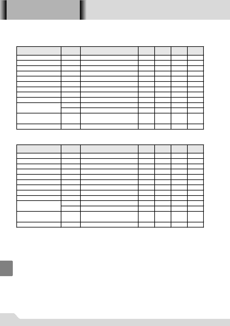
PARAMETER
SYMBOL
MIN
TYP
MAX
UNITS
Operating Voltage
4.5
5.0
5.5
2.4
0.4
CMOS: V
DD
=4.5V, I
OH
=-16mA
3.9
4.2
CMOS: V
DD
=4.5V, I
OL
=16mA
0.3
0.4
Consumption Current 1
35
mA
Consumption Current 2
5
mA
0.5
1.0
2.0
M
25
50
100
k
Cg
13
pF
Cd
13
pF
Internal Oscillation Feedback
Resistance
Rf
100
240
400
k
10
µA
/INH="L"
Internal Oscillation
Capacitance
(note 3)
(note 3)
CONDITIONS
/INH="L"
PARAMETER
SYMBOL
MIN
TYP
MAX
UNITS
Operating Voltage
2.97
3.3
3.63
2.4
0.4
CMOS: V
DD
=2.97V, I
OH
=-8mA
2.47
CMOS: V
DD
=2.97V, I
OL
=8mA
0.4
Consumption Current 1
10
mA
Consumption Current 2
1
mA
1.0
2.0
4.0
M
35
70
140
k
Cg
13
pF
Cd
13
pF
Internal Oscillation Feedback
Resistance
Rf
0.3
1.0
2.0
M
10
µA
/INH="L"
Internal Oscillation
Capacitance
(note 3)
(note 3)
/INH="L"
CONDITIONS
3.3V, f0 x 8 multiplier (note 1)
Ta=25
Ta=25
5.0V, f0 x 8 multiplier (note 2)
V
DD
V
IH
V
IL
V
OH
V
OL
I
DD
1
I
DD
2
Rup1
Rup2
Output Off Leak Current
Input pull up resistance 2
Input pull up resistance 1
'L' Level Output Voltage
'H' Level Output Voltage
'L' Level Input Voltage
'H' Level Input Voltage
/INH="OPEN", C
L
=15pF, f=80MHz
Ioz
/INH=0.7V
DD
/INH="L", C
L
=15pF, f=80MHz
note 1 : The output frequency range is 80 MHz to 100MHz with a multiplier of f0 x 8 at 3.3V
note 2 : The output frequency range is 80 MHz to 160MHz with a multiplier of f0 x 8 at 5.0V
note 3 : measured value
'H' Level Input Voltage
'L' Level Input Voltage
'H' Level Output Voltage
'L' Level Output Voltage
Input pull up resistance 1
Input pull up resistance 2
Output Off Leak Current
V
DD
V
IH
V
IL
V
OH
V
OL
I
DD
1
I
DD
2
Rup1
Rup2
Ioz
/INH="OPEN", C
L
=15pF, f=160MHz
/INH="L", C
L
=15pF, f=160MHz
/INH=0.7V
DD
Electrical Characteristics
XC2173
Series
1041
14
Rup
Cg
Cd
Rf
XT
/XT
/INH
1/2
1/2
1/2
PLL
PARAMETER
SYMBOL
CONDITIONS
UNITS
Supply Voltage
V
Input Voltage
V
Power Dissipation
Pd
mW
Operating Ambient Temp.
Topr
Storage Temp.
Tstg
V
SS
-0.3V
SS
+7.0
V
SS
-0.3V
DD
+0.3
250 (*3)
-40+85
-55+125
V
DD
V
IN
* When measured on a glass epoxy PCB
/INH Qo
Q
O
V
SS
V
DD
Absolute Maximum Ratings
Block Diagram
14S_05XC2173 02.09.12 16:37 1041
XC2173
Series
1042
14
PARAMETER
SYMBOL
MIN
TYP
MAX
UNITS
Operating Voltage
4.5
5.0
5.5
2.4
0.4
CMOS: V
DD
=4.5V, I
OH
=-16mA
3.9
4.2
CMOS: V
DD
=4.5V, I
OL
=16mA
0.3
0.4
Consumption Current 1
28
mA
Consumption Current 2
5
mA
0.5
1.0
2.0
M
25
50
100
k
Cg
13
pF
Cd
13
pF
Internal Oscillation Feedback
Resistance
Rf
100
240
400
k
10
µA
/INH="L"
Internal Oscillation
Capacitance
(note 3)
(note 3)
/INH="L"
CONDITIONS
PARAMETER
SYMBOL
MIN
TYP
MAX
UNITS
Operating Voltage
2.97
3.3
3.63
2.4
0.4
CMOS: V
DD
=2.97V, I
OH
=-8mA
2.47
CMOS: V
DD
=2.97V, I
OL
=8mA
0.4
Consumption Current 1
9
mA
Consumption Current 2
1
mA
1.0
2.0
4.0
M
35
70
140
k
Cg
13
pF
Cd
13
pF
Internal Oscillation Feedback
Resistance
Rf
0.3
1.0
2.0
M
10
µA
/INH="L"
Internal Oscillation
Capacitance
(note 3)
(note 3)
CONDITIONS
Ta=25
Ta=25
3.3V, f0 x 7 multiplier (note 1)
5.0V, f0 x 7 multiplier (note 2)
note 1 : The output frequency range is 70 MHz to 100MHz with a multiplier of f0 x 7 at 3.3V
note 2 : The output frequency range is 80 MHz to 160MHz with a multiplier of f0 x 7 at 5.0V
note 3 : measured value
V
DD
V
IH
V
IL
V
OH
V
OL
I
DD
1
I
DD
2
Rup1
Rup2
Ioz
'H' Level Input Voltage
'L' Level Input Voltage
'H' Level Output Voltage
'L' Level Output Voltage
Input pull up resistance 1
Input pull up resistance 2
Output Off Leak Current
/INH="OPEN", C
L
=15pF, f=140MHz
/INH="L", C
L
=15pF, f=140MHz
/INH=0.7V
DD
'H' Level Input Voltage
'L' Level Input Voltage
'H' Level Output Voltage
'L' Level Output Voltage
Input pull up resistance 1
Input pull up resistance 2
Output Off Leak Current
V
DD
V
IH
V
IL
V
OH
V
OL
I
DD
1
I
DD
2
Rup1
Rup2
Ioz
/INH="OPEN", C
L
=15pF, f=70MHz
/INH="L", C
L
=15pF, f=70MHz
/INH="L"
/INH=0.7V
DD
14S_05XC2173 02.09.12 16:37 1042

XC2173
Series
1043
14
PARAMETER
SYMBOL
MIN
TYP
MAX
UNITS
Operating Voltage
4.5
5.0
5.5
2.4
0.4
CMOS: V
DD
=4.5V, I
OH
=-16mA
3.9
4.2
CMOS: V
DD
=4.5V, I
OL
=16mA
0.3
0.4
Consumption Current 1
23
mA
Consumption Current 2
5
mA
0.5
1.0
2.0
M
25
50
100
k
Cg
13
pF
Cd
13
pF
Internal Oscillation Feedback
Resistance
Rf
100
240
400
k
10
µA
/INH="L"
Internal Oscillation
Capacitance
(note 3)
(note 3)
/INH="L"
CONDITIONS
PARAMETER
SYMBOL
MIN
TYP
MAX
UNITS
Operating Voltage
2.97
3.3
3.63
2.4
0.4
CMOS: V
DD
=2.97V, I
OH
=-8mA
2.47
CMOS: V
DD
=2.97V, I
OL
=8mA
0.4
Consumption Current 1
8
mA
Consumption Current 2
1
mA
1.0
2.0
4.0
M
35
70
140
k
Cg
13
pF
Cd
13
pF
Internal Oscillation Feedback
Resistance
Rf
0.3
1.0
2.0
M
10
µA
/INH="L"
/INH="L"
Internal Oscillation
Capacitance
(note 3)
(note 3)
CONDITIONS
Ta=25
Ta=25
3.3V, f0 x 6 multiplier (note 1)
5.0V, f0 x 6 multiplier (note 2)
'H' Level Input Voltage
'L' Level Input Voltage
'H' Level Output Voltage
'L' Level Output Voltage
Input pull up resistance 1
Input pull up resistance 2
Output Off Leak Current
Ioz
Rup2
Rup1
I
DD
2
I
DD
1
V
OL
V
OH
V
IL
V
IH
V
DD
/INH="OPEN", C
L
=15pF, f=120MHz
/INH="L", C
L
=15pF, f=120MHz
/INH=0.7V
DD
note 1 : The output frequency range is 60 MHz to 100MHz with a multiplier of f0 x 6 at 3.3V
note 2 : The output frequency range is 80 MHz to 150MHz with a multiplier of f0 x 6 at 5.0V
note 3 : measured value
'H' Level Input Voltage
'L' Level Input Voltage
'H' Level Output Voltage
'L' Level Output Voltage
Input pull up resistance 1
Input pull up resistance 2
Output Off Leak Current
V
DD
V
IH
V
IL
V
OH
V
OL
I
DD
1
I
DD
2
Rup1
Rup2
Ioz
/INH="OPEN", C
L
=15pF, f=60MHz
/INH="L", C
L
=15pF, f=60MHz
/INH=0.7V
DD
14S_05XC2173 02.09.12 16:37 1043