12S_00flà
1.2V Input / Output Rail To Rail CMOS Op Amp
Series
881
12
The XC221A1200MR is an input / output rail to rail CMOS Op Amp.
With rail to rail functions, operation is guaranteed from power supplies as
low as 1.2V. Moreover, since the XC221 comes in an ultra small SOT-25
package, the series is particularly suited for use with various types of
portable phones.
Bandwidths of 550kHz and slew rates of 0.5V can be achieved even with
power consumption as low as 100
µA.
Even with large capacitance levels of C
L
= 200pF (unity gain connection),
the XC221 will not be susceptible to oscillation.
General Description
Operating Voltage Range : 1.2 ~ 10V ( single cell )
: ± 0.6 ~ 5V ( + ve / - ve supply )
Output Signal
: 0.1 ~ 2.9V (3V single cell, R
L
=2k )
Gain Bandwidth
: 550kHz (15
µA: 210kHz)
Slew Rate
: 0.5V /
µS
High Capacitance Load
: C
L
=200pF
Low Supply Current
: 100
µA, 15µA
Ultra Small Package
: SOT-25 mini mold
GPalmtop computers, PDAs
GCellular and portable phones
GPortable audio systems
GVarious battery powered systems
Features
Applications
NOperating Voltage Range (Single Cell)
: 1.2V ~ 10V
NInput / Output Rail To Rail Operation
NGain Bandwidth
: 550kHz
NSlew Rate
: 0.5V /
µS
NLow Power Consumption : 100µA
NSOT - 25 Ultra Small Package
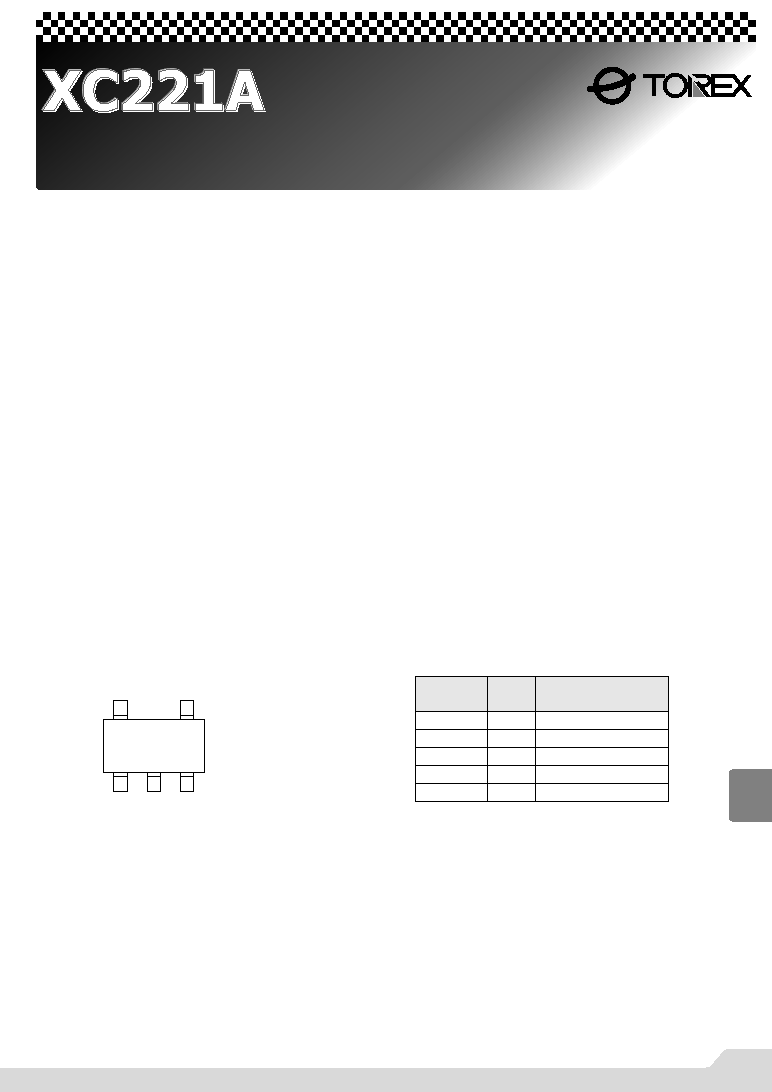
1
SOT-25
(TOP VIEW)
IN+
IN-
V
SS
V
OUT
V
DD
Pin Configuration
Pin Assignment
SYMBOL
1
2
3
4
Positive Input
Negative Input
Negative Power Supply Pin
5
FUNCTION
PIN NUMBER
Output Pin
Positive Power Supply Pin
V
OUT
V
DD
IN+
IN-
V
SS
12S_01XC221A 02.09.12 15:47 881
XC221A
Series
882
12
Product Classification
GOrdering Information
SYMBOL
DESCRIPTION
SYMBOL
DESCRIPTION
Represents the number of channels:
Package Type
1 = one
SOT-25
Represents the supply current.
1 = 15
µA
2 = 100
µA
0 = Internal Standard
Device Orientation
Embossed Tape (Right)
Embossed Tape (Left)
Load Capacitance:
0 = 200pF
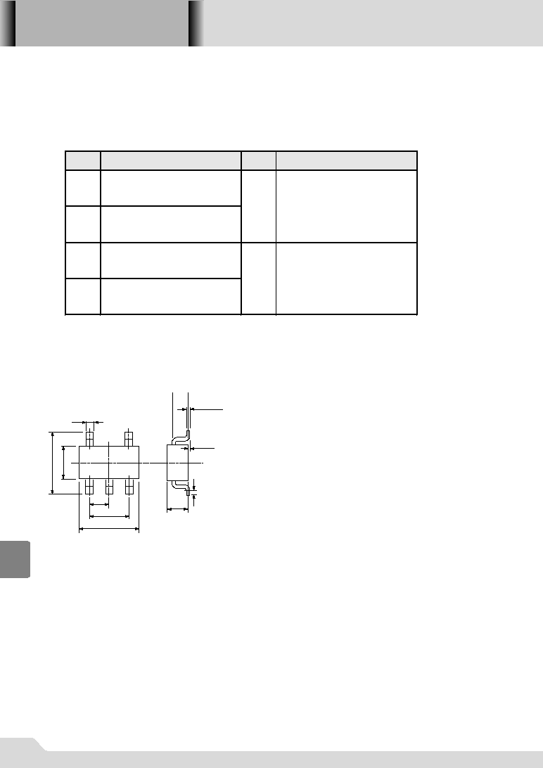
Packaging Information
GSOT-25
0.4
0.95
1.9±0.2
2.9±0.2
+0.1
-0.05
1.1±0.1
00.1
0.15
0.2min
+0.1
-0.05
2.8±0.2
1.6
+0.2
-0.1
12S_01XC221A 02.09.12 15:47 882
XC221A
Series
883
12
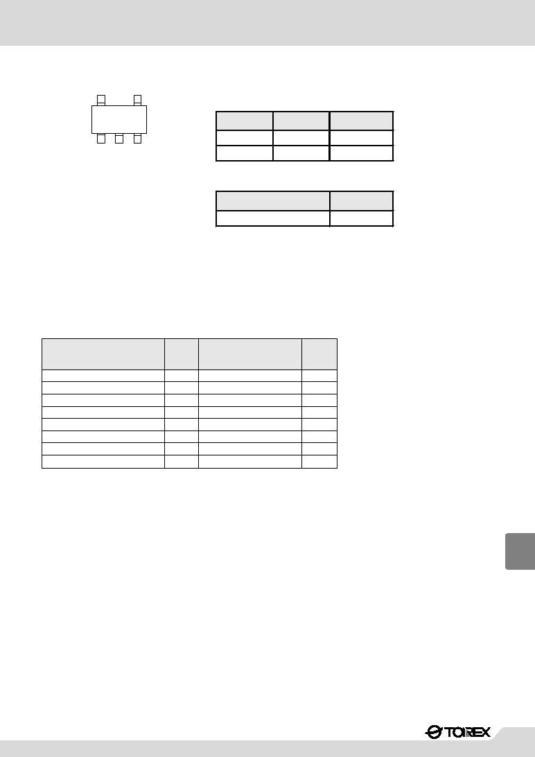
Marking
Load Capacitance
DESIGNATOR
200pF
0
SOT-25
(TOP VIEW)
q w e r
qRepresents the product name and the supply current.
eRepresents load capacitance
rDenotes the production lot number
0 to 9, A to Z repeated(G.I.J.O.Q.W excepted)
wBased on internal standards
PRODUCT
NAME
SUPPLY
CURRENT
DESIGNATOR
XC221A11
15A
1
XC221A12
100A
2
RAIL-TO-RAIL is a trademark of Motolola.
Ta = 25, V
SS
= 0V
OUT pin voltage
IN pin voltage
IN/ pin voltage
OUT pin current
Continuous Total Power Dissipation
Ambient Operating Temp.
Storage Temp.
PARAMETER
V
DD
pin voltage
SYMBOL
Topr
Tstg
V
DD
V
OUT
V
IN
+
V
IN
-
I
OUT
Pd
UNITS
V
V
V
V
mA
mW
RATINGS
-0.3 12
-0.3 12
±100
150
-30 +80
-40 +125
-0.3V
DD
+0.3
-0.3V
DD
+0.3
Absolute Maximum Ratings
12S_01XC221A 02.09.12 15:47 883
XC221A
Series
884
12
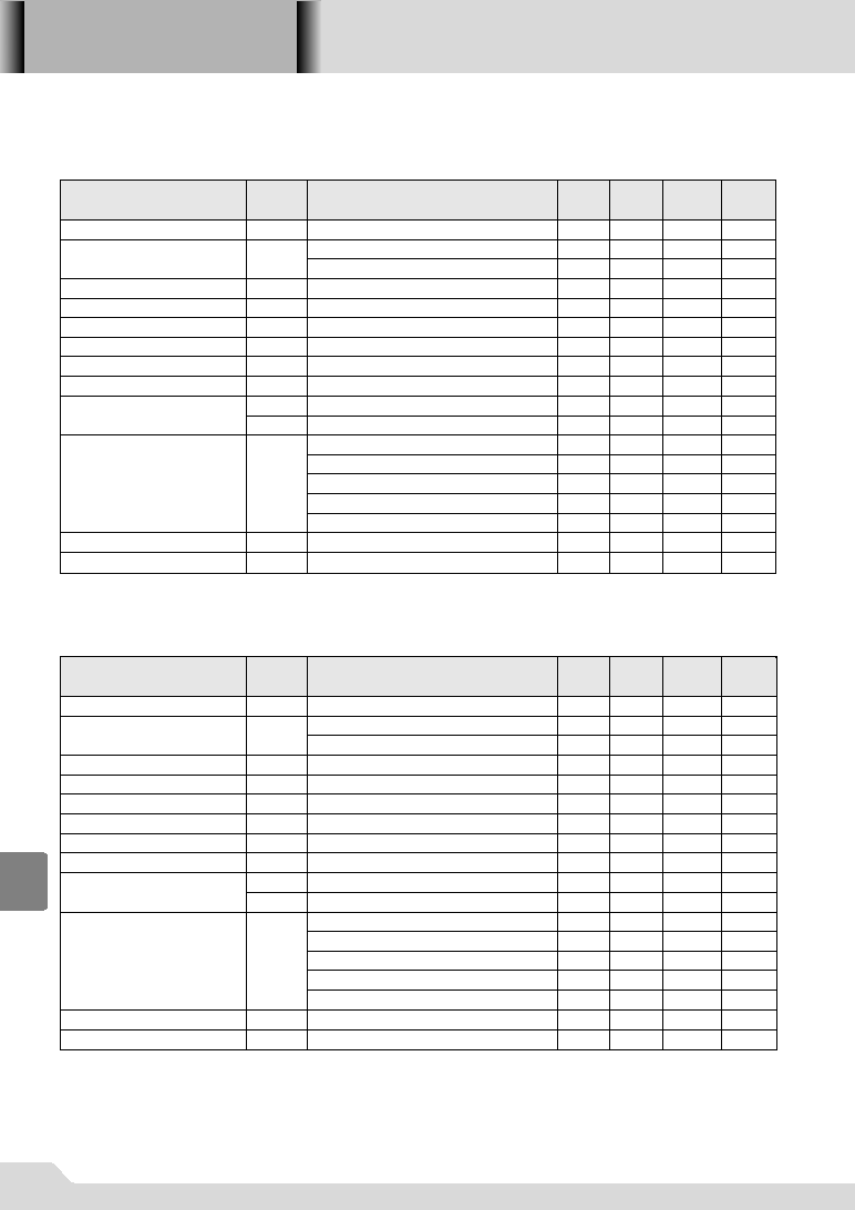
Electrical Characteristics
XC221A1100
Ta = 25
XC221A1200
Ta = 25
I
DD
=
15
µA
Measuring Conditions :
Unless otherwise stated, V
DD
= 3.0V, V
SS
= 0V, V
CM
= V
OUT
= V
DD
/ 2, R
L
= 1M
(to V
SS
), C
L
= 10pF (to V
SS
)
I
DD
=
100
µA
Measuring Conditions :
Unless otherwise stated, V
DD
= 3.0V, V
SS
= 0V, V
CM
= V
OUT
= V
DD
/ 2, R
L
= 1M
(to V
SS
), C
L
= 10pF (to V
SS
)
Power Supply Voltage Range
Supply Current
Input Offset Voltage
Input Offset Current
Input Bias Current
Input Resistance
Large Signal Voltage Gain
Common Mode Rejection Ratio
Power Supply Rejection Ratio
Output Voltage Range
Gain Bandwidth
Slew Rate
PARAMETER
SYMBOL
CMRR
SR
V
DD
I
DD
V
OF
I
OF
I
B
R
IN
AVD
PSRR+
PSRR-
V
OUT
FT
CONDITIONS
V
DD
= 3V
V
DD
= 1.2V
0
V
CM
3.0V
V
DD
= 3 to 10V, V
SS
= 0V, V
OUT
= 1.5V
V
SS
= -3 to -10V, V
DD
= 0V, V
OUT
= -1.5V
R
L
=
V
DD
= 1.2V, R
L
= 47k (to V
DD
/2)
V
DD
= 3V, R
L
= 2k(to V
DD
/2)
V
DD
= 5V, R
L
= 2k(to V
DD
/2)
V
DD
= 10V, R
L
= 2k(to V
DD
/2)
V
DD
= 3V
V
DD
=3 V
UNITS
V
µA
µA
T
V
V
V
V
V
V/
µsec
mV
pA
pA
dB
dB
dB
dB
kHz
UNITS
V
µA
µA
T
V
V
V
V
V
V/
µsec
mV
pA
pA
dB
dB
dB
dB
kHz
MAX
10
23
23
20.0
-
-
-
-
-
-
-
1.10
2.90
4.90
9.80
-
-
V
DD
-0.05
MAX
10
150
150
20.0
-
-
-
-
-
-
-
1.10
2.90
4.90
9.80
-
-
V
DD
-0.05
TYP
-
15
8
-
1
1
1
110
75
75
75
-
-
-
-
-
210
0.07
TYP
-
100
50
-
1
1
1
110
75
75
75
-
-
-
-
-
550
0.50
MIN
1.2
10
2.5
-
-
-
-
75
60
60
60
0.05
0.10
0.10
0.10
0.10
-
-
MIN
1.2
67
16.75
-
-
-
-
75
60
60
60
0.05
0.10
0.10
0.10
0.10
-
-
V
DD
= 3V
V
DD
= 1.2V
0
V
CM
3.0V
V
DD
= 3 to 10V, V
SS
= 0V, V
OUT
= 1.5V
V
SS
= -3 to -10V, V
DD
= 0V, V
OUT
= -1.5V
R
L
=
V
DD
= 1.2V, R
L
= 47k (to V
DD
/2)
V
DD
= 3V, R
L
= 2k(to V
DD
/2)
V
DD
= 5V, R
L
= 2k(to V
DD
/2)
V
DD
= 10V, R
L
= 2k(to V
DD
/2)
V
DD
= 3V
V
DD
= 3V
CONDITIONS
Power Supply Voltage Range
Supply Current
Input Offset Voltage
Input Offset Current
Input Bias Current
Input Resistance
Large Signal Voltage Gain
Common Mode Rejection Ratio
Power Supply Rejection Ratio
Output Voltage Range
Gain Bandwidth
Slew Rate
SYMBOL
CMRR
SR
V
DD
I
DD
V
OF
I
OF
I
B
R
IN
AVD
PSRR+
PSRR-
V
OUT
FT
PARAMETER
12S_01XC221A 02.09.12 15:47 884
XC221A
Series
885
12
0.01
0.1
1
10
100
0.001
0.01
0.1
1
10
XC221A1100
0.01
0.1
1
10
100
0.001
0.01
0.1
1
10
XC221A1100
0
5
10
15
20
25
30
35
40
0
2
4
6
8
10
XC221A1100
Topr=25
80
-30
0
5
10
15
20
25
30
35
-40
-20
0
20
40
60
80
XC221A1100
5V
3V
-20
-10
0
10
20
30
40
10
100
1000
10000
-150
-100
-50
0
50
100
150
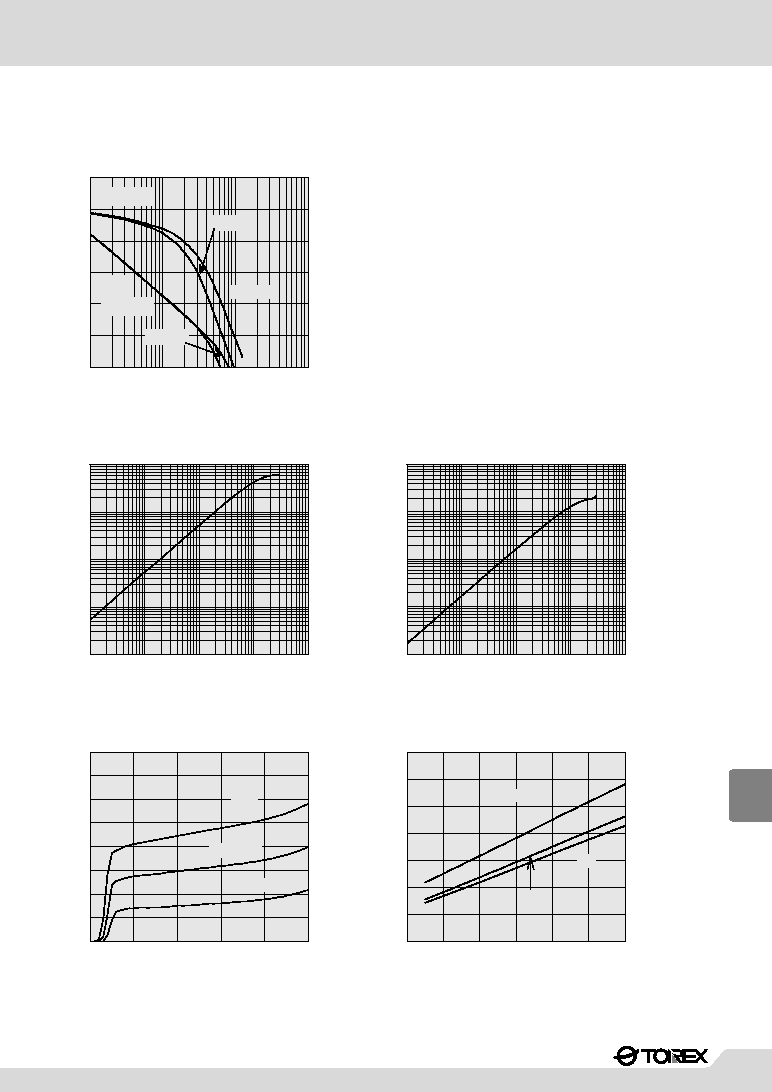
(1) VOLTAGE GAIN, PHASE MARGIN
(4) SUPPLY CURRENT vs. POWER SUPPLY VOLTAGE
(5) SUPPLY CURRENT vs. AMBIENT TEMPERATURE
XC221A1100
V
DD
/V
SS
=±1.5V
R
L
=2K
Gain (dB)
Frequency (kHz)
Phase margin (°)
C
L
=200pF
C
L
=10pF
C
L
=200pF
C
L
=10pF
(2) SINK CURRENT vs. OUTPUT VOLTAGE
V
DD
=3V
Sink Current:I
SINK
(mA)
Output Voltage:V
OUT
(V)
(3) SOURCE CURRENT vs. OUTPUT VOLTAGE
V
DD
=3V
Source Current:I
SOURCE
(mA)
Power Supply - Output Voltage Diff. :V
DD
-V
OUT
(V)
V
IN
=V
DD
/2
Power Supply Voltage:V
DD
(V)
Supply Current:I
DD
(A)
V
IN
=V
DD
/2
V
DD
=10V
Ambient Temp.:Topr()
Supply Current:I
DD
(A)
XC221A1100 (15 A) Typical Performance Characteristics
12S_01XC221A 02.09.12 15:47 885