
1
XC6109 ETR0206_002.doc
CMOS
Highly Accurate
: +2%
Low Power Consumption : 0.9
µA (TYP.)
(V
DF
=1.9V, V
IN
= 2.0V)
Built-In Delay Circuit, Delay Pin Available
GENERAL DESCRIPTION
The XC6109 series is highly precise, low power
consumption voltage detector, manufactured using CMOS
and laser trimming technologies.
With the built-in delay circuit, connecting the delay
capacitance pin to the capacitor enables the IC to provide an
arbitrary release delay time.
Using an ultra small package (SSOT-24), the series is suited
for high density mounting.
Both CMOS and N-channel open drain output configurations
are available.
APPLICATIONS
Microprocessor reset circuitry
Charge voltage monitors
Memory battery back-up switch circuits
Power failure detection circuits
TYPICAL APPLICATION CIRCUIT
FEATURES
Highly Accurate :
+
2%
(Setting Voltage Accuracy>1.5V)
:
+30mV
(Setting
Voltage
Accuracy<1.5V)
Low Power Consumption : 0.9
µA
(TYP.,
V
DF
=1.9V, V
IN
= 2.0V)
Detect Voltage Range
: 0.8V ~ 5.0V
in 100mV increments
Operating Voltage Range
: 0.7V ~ 6.0V
Detect Voltage Temperature Characteristics
:
±100ppm/
O
C (TYP.)
Output Configuration
: CMOS or
N-channel open drain
Operating Temperature Range : -40
O
C ~ +85
O
C
Ultra Small Package :
SSOT-24
VIN
Cd
VSS
VOUT
Cd
R=100k
VIN
(No resistor needed for
CMOS output products)
TYPICAL PERFORMANCE
CHARACTERISTICS
Release Delay Time vs. Delay Capacitance
XC6109xxxAN
0.1
1
10
100
1000
10000
0.0001
0.001
0.01
0.1
1
Delay Capacitance: Cd (µF)
Re
l
e
a
s
e
D
e
l
a
y
T
i
m
e
:
T
D
R
(m
s
)
VIN(MIN.)=0.7V,VIN(MAX.)=6.0V
Tr=5µs, Ta=25
2
XC6109
Series
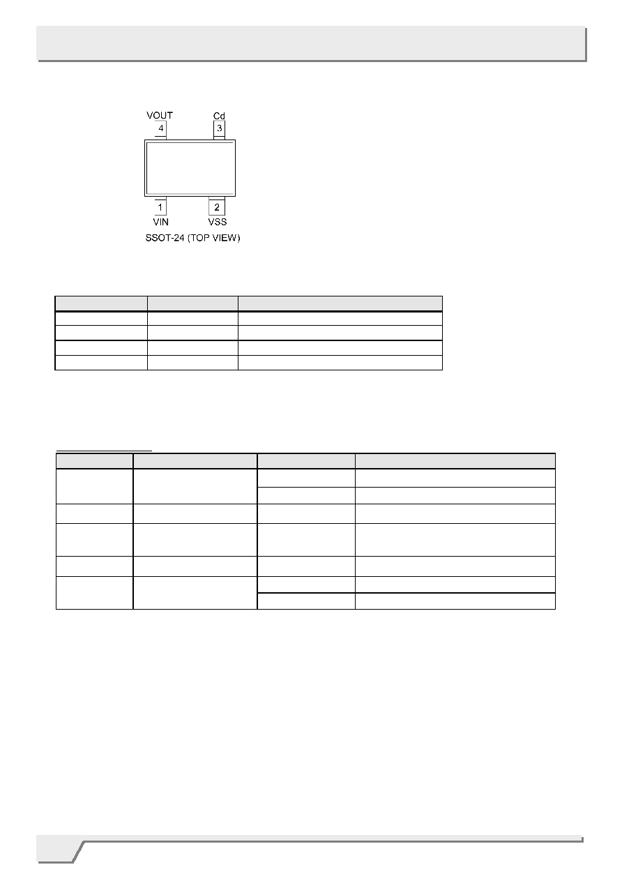
PIN NUMBER
PIN NAME
FUNCTION
1 V
IN
Input
2 V
SS
Ground
3 Cd
Delay
Capacitance
4 V
OUT
Output (Detect "L")
DESIGNATOR
DESCRIPTION
SYMBOL
DESCRIPTION
C
: CMOS output
Output
Configuration
N
: N-ch open drain output
Detect Voltage
08 ~ 50
: e.g. 181.8V
Output Delay & Hysteresis
A
: Built-in delay pin & hysteresis 5% (TYP.)
Package N
:
SSOT-24
R
: Embossed tape, standard feed
Device
Orientation
L
: Embossed tape, reverse feed
PIN CONFIGURATION
PIN ASSIGNMENT
PRODUCT CLASSIFICATION
XC6109
Ordering Information
3
XC6109
Series
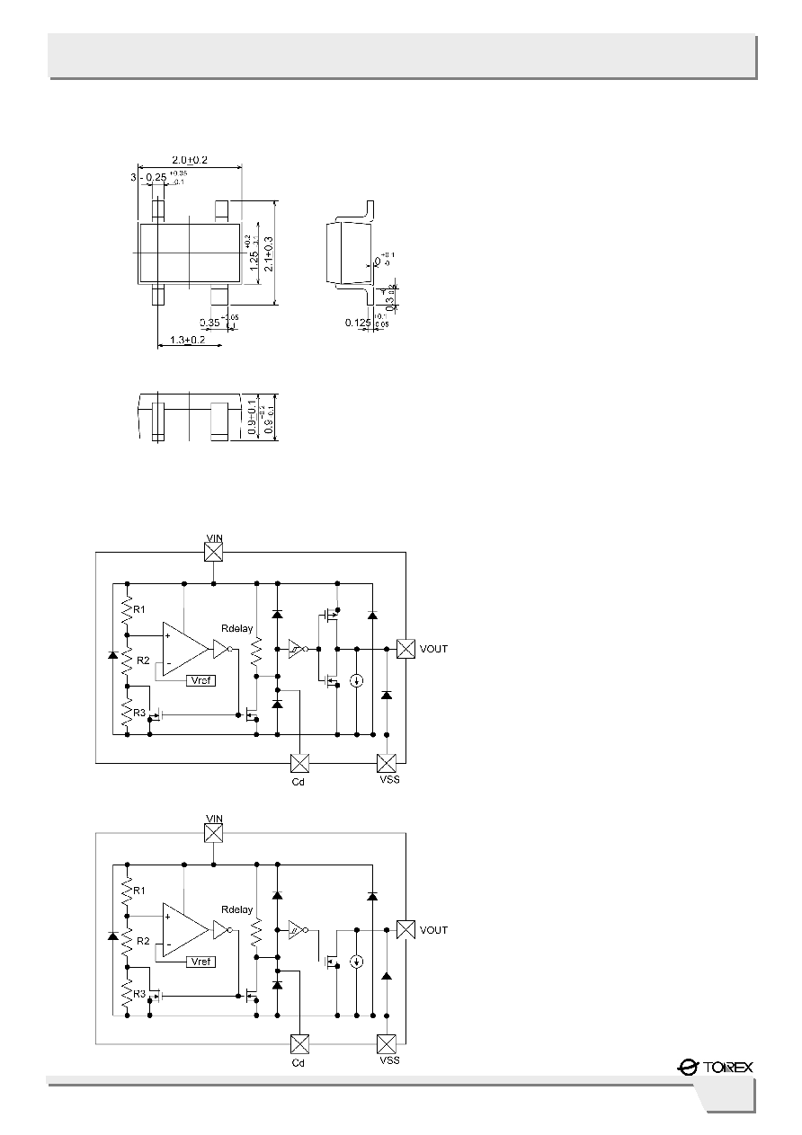
PACKAGING INFORMATION
SSOT-24
BLOCK DIAGRAMS
(1) XC6109C (CMOS Output)
(2) XC6109N (N-ch Open Drain Output)

4
XC6109
Series
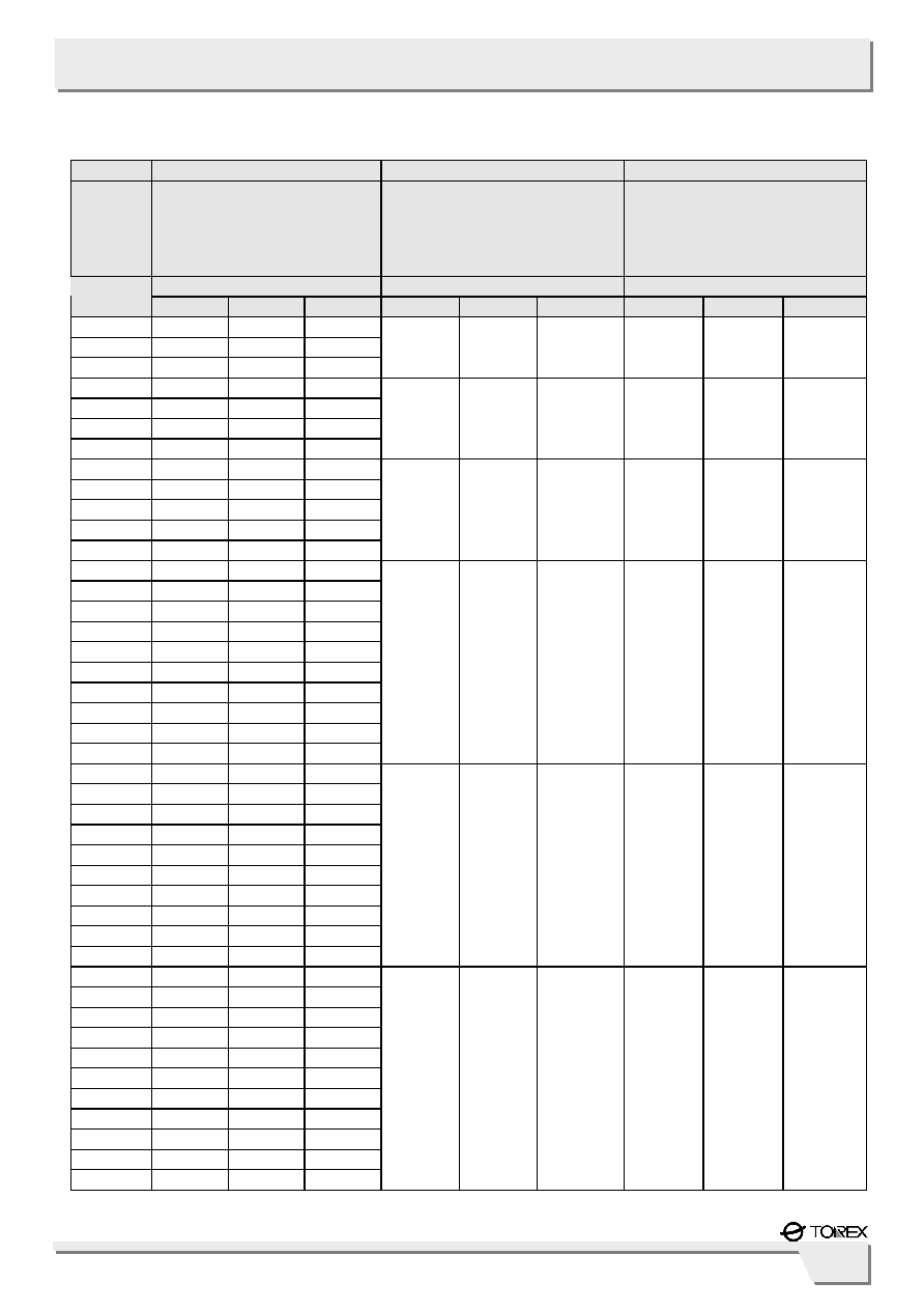
PARAMETER
SYMBOL
CONDITIONS
MIN.
TYP.
MAX.
UNIT
CIRCUIT
Operating Voltage
V
IN
V
DF(T)=
0.8~5.0V
(*1)
0.7 - 6.0 V -
Detect Voltage
V
DF
V
DF(T)=
0.8~5.0V E-1
V
1
Hysteresis Range 1
V
HYS1
V
IN
=1.0~6.0V
V
DF
x 0.02
V
DF
x 0.05
V
DF
x 0.08
V 1
V
DF(T)=
0.8~1.9V
- 0.80
1.70
V
DF(T)=
2.0~3.9V
- 0.90
1.90
Supply Current 1
I
SS1
V
IN
=V
DF
x 0.9
V
DF(T)=
4.0~5.0V
- 1.00
2.00
µA
2
V
DF(T)=
0.8~1.9V
- 0.90
1.80
V
DF(T)=
2.0~3.9V
- 1.10
2.00
Supply Current 2
I
SS2
V
IN
=V
DF
x 1.1
V
DF(T)=
4.0~5.0V
- 1.20
2.20
µA
2
I
OUT1
V
IN
=V
DF
x0.9
V
DS
=0.5V (N-ch)
E-2
mA 3
Output Current
I
OUT2
(*2)
V
IN
=V
DF
x1.1
V
DS
=0.5V (P-ch)
E-3
mA 3
V
DF
Temperature
Characteristics
TaV
DF
-40
O
C
<Ta<85
O
C
-
±
100
-
ppm/
O
C
1
Delay Resistance (*3)
Rdelay
V
IN
=6.0V, V
CD
=0V
1.6 2.0 2.4 M
4
Delay Pin Sink Current
I
CD
V
DS
=0.5V, V
IN
=0.7V 8
60
-
µA
4
V
IN
=1.0V
0.4 0.5 0.6
Delay Capacitance Pin
Threshold Voltage
V
TCD
V
IN
=6.0V
2.9 3.0 3.1
V 5
Unspecified Operating
Voltage (*4)
V
UNS
V
IN
=0~0.7V -
0.3
0.4
V
6
Detect Delay Time (*5)
T
DF0
V
IN
=6.0 down to 0.7V
Cd: Open
- 30
230
µs
7
Release Delay Time
(*6)
T
DR0
V
IN
=0.7~6.0V
Cd: Open
- 30
200
µs
7
PARAMETER
SYMBOL
RATINGS
UNITS
Input Voltage
V
IN
V
SS
- 0.3 ~ 7.0
V
Output Current
I
OUT
10
mA
XC6109C (
*1
) V
SS
- 0.3 ~ V
IN
+ 0.3
Output Voltage
XC6109N (
*2
)
V
OUT
V
SS
- 0.3 ~ 7.0
V
Delay Pin Voltage
V
CD
V
SS
-0.3 ~ V
IN
+ 0.3
V
Delay Pin Current
I
CD
5.0 mA
Power Dissipation
SSOT-24
Pd
150
mW
Operating Temperature Range
Ta
- 40 ~ + 85
O
C
Storage Temperature Range
Tstg
- 40 ~ + 125
O
C
ABSOLUTE MAXIMUM RATINGS
Ta = 25
O
C
ELECTRICAL CHARACTERISTICS
Ta = 25
O
C
NOTE:
*1: V
DF(T):
Setting Detect Voltage
*2: This numerical value is applied only to the XC6109C series (CMOS output).
*3: Calculated from the voltage value and the current value of both ends of the resistor.
*4: The maximum voltage of the V
OUT
in the range of the V
IN
0 to 0.7V.
This numerical value is applied only to the XC6109C series
(CMOS output).
*5: Time which ranges from the state of V
IN
=V
DF
to the V
OUT
reaching 0.6V when the V
IN
falls without connecting to the Cd pin.
*6: Time which ranges from the state of V
IN
= V
DF
+V
HYS
to the V
OUT
reaching 5.4V when the V
IN
rises without connecting to the Cd pin.
NOTE:
*1: CMOS output
*2: N-ch open drain output
5
XC6109
Series
SYMBOL
E-1
E-2
E-3
SETTING
OUTPUT
VOLTAGE
(V)
DETECT VOLTAGE (*1)
(V)
OUTPUT CURRENT
(mA)
OUTPUT CURRENT (*2)
(mA)
V
DF
I
OUT
1
I
OUT
2
V
DF
(T)
MIN.
TYP.
MAX.
MIN.
TYP.
MAX.
MIN.
TYP.
MAX.
0.8 0.770 0.800 0.830
0.9 0.870 0.900 0.930
1.0 0.970 1.000 1.030
0.01 0.36 0.70 -0.40 -0.20 -0.01
1.1 1.070 1.100 1.130
1.2 1.170 1.200 1.230
1.3 1.270 1.300 1.330
1.4 1.370 1.400 1.430
0.10 0.70 1.30 -0.60 -0.30 -0.08
1.5 1.470 1.500 1.530
1.6 1.568 1.600 1.632
1.7 1.666 1.700 1.734
1.8 1.764 1.800 1.836
1.9 1.862 1.900 1.938
0.30 1.00 1.80 -0.80 -0.40 -0.14
2.0 1.960 2.000 2.040
2.1 2.058 2.100 2.142
2.2 2.156 2.200 2.244
2.3 2.254 2.300 2.346
2.4 2.352 2.400 2.448
2.5 2.450 2.500 2.550
2.6 2.548 2.600 2.652
2.7 2.646 2.700 2.754
2.8 2.744 2.800 2.856
2.9 2.842 2.900 2.958
0.60 1.60 2.60 -1.00 -0.50 -0.20
3.0 2.940 3.000 3.060
3.1 3.038 3.100 3.162
3.2 3.136 3.200 3.264
3.3 3.234 3.300 3.366
3.4 3.332 3.400 3.468
3.5 3.430 3.500 3.570
3.6 3.528 3.600 3.672
3.7 3.626 3.700 3.774
3.8 3.724 3.800 3.876
3.9 3.822 3.900 3.978
1.00 2.00 3.10 -1.20 -0.60 -0.40
4.0 3.920 4.000 4.080
4.1 4.018 4.100 4.182
4.2 4.116
4.200
4.284
4.3 4.214 4.300 4.386
4.4 4.321 4.400 4.488
4.5 4.410 4.500 4.590
4.6 4.508 4.600 4.692
4.7 4.606 4.700 4.794
4.8 4.704 4.800 4.896
4.9 4.802 4.900 4.998
5.0 4.900 5.000 5.100
1.30 2.30 3.30 -1.30 -0.65 -0.60
VOLTAGE CHART
NOTE:
*1: When V
DF(T)
1.4V, the detection accuracy is ±30mV. When V
DF(T)
1.5V, the detection accuracy is ±2%.
*2: This numerical value is applied only to the XC6109C series (CMOS output).