Positive Voltage Regulators (Output On/Off)
Series
315
3
General Description
Features
Applications
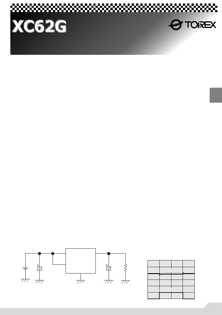
Typical Application Circuit
Typical Performance
Characteristic
The XC62G series are highly precise, low power consumption positive
voltage regulators, manufactured using CMOS and laser trimming
technologies. The series achieves high output currents, with low input-
output voltage differentials, and consists of a high precision voltage
reference, an error correction circuit, and an output driver with current
limitation. With good transient responses, output remains stable even
during load changes. Also, having high ripple rejection ratios, the series
can be used with low power supply noise. The CE input enables the
output to be turned off, resulting in reduced power consumption. SOT-25
(150mW) and SOT-89-5 (500mW) packages are available. With regards
to the CE function, as well as the positive logic XC62GR series, a
negative logic XC62GP series (custom) is also available.
Maximum Output Current
: 150mA (within max. power
dissipation,V
OUT
=3.0V)
Output Voltage Range : 2.1V~5.0V in 0.1V increments
Highly Accurate
: Set-up voltage ±2%
(±1% for semi-custom products)
Low Power Consumption
: TYP. 13
µA (V
OUT
= 3.0V),
TYP 23
µA (V
OUT
=3.0V semi-custom,
high-speed versions),
TYP 0.1
µA (Stand-by mode)
Output Voltage Temperature Characteristics
: TYP ±100ppm/∞C
Input Stability
: TYP 0.2%/V
Ultra Small Packages : SOT-25 (150mW) mini-mold
SOT-89-5 (500mW) mini-power mold
GBattery-powered Equipment
GVoltage supplies for cellular phones
GCameras, Video Recorders
GPalmtops
NCMOS Low Power Consumption
NSmall Input-Output Voltage Differential
: 0.2V @ 80mA,
0.38V @ 160mA
NMaximum Output Current
: 150mA (V
OUT
= 3.0V)
NHighly Accurate : ±2% (±1%)
NOutput Voltage Range
: 2.1V ~ 5.0V
NStand-by Supply Current
: 0.1
µA (V
OUT
= 3.0V)
NSOT-25 / SOT-89-5 Package
R
L
V
IN
V
IN
CE
V
SS
V
OUT
C
IN
4.7
µF
Tantalum
C
L
10
µF
Tantalum
Output Voltage
Output Voltage
4.6
4.7
4.8
5.0
4.9
5.1
5.2
0
40
80
120
160
200
240
Output Voltage:V
OUT
V
Output Current:I
OUT
m
A
Time2msec/div
XC62GR50225V HIGH SPEED
V
IN
6V , C
L
10
µFtantalum
40mA
1mA
03S_07XC62G 02.9.12 3:04 PM 315

XC62G
Series
316
3
Pin Configuration
Pin Assignment
SOT-25
TOP VIEW
SOT-89-5
TOP VIEW
5
5
4
4
3
1
2
V
OUT
V
SS
V
OUT
V
SS
NC
V
IN
CE
NC
V
IN
CE
1
3
2
PIN NUMBER
SOT-25
SOT-89-5
PIN NAME
FUNCTION
1
4
Ground
Chip Enable
2
2
V
SS
3
3
Supply Voltage input
V
IN
4
1
No Connection
5
5
(NC)
Regulated Output Voltage
V
OUT
CE
Product Classification
GOrdering Information
DESIGNATOR
a
e
f
b
c
d
DESCRIPTION
DESIGNATOR
DESCRIPTION
True Logic Level at CE Pin:
R=Positive
P=Negative(Custom)
Output Voltage
30=3.0V
50=5.0V
Response:
1=Standard
2=High Speed (Semi-Custom)
Output Voltage Accuracy:
1=
±1.0%(Semi-custom)
2=
±2.0%
Package Type
M=SOT-25
P=SOT-89-5
Device Orientation
R=Embossed Tape
(Standard Feed)
L=Embossed Tape
(Reverse Feed)
X C 6 2 G X X X X X X X
a
b
c
d
e
f
Function List
H=High, L=Low
SERIES
CE
VOLTAGE OUTPUT
XC62GR
H
ON
L
OFF
XC62GP
H
OFF
L
ON
03S_07XC62G 02.9.12 3:04 PM 316

XC62G
Series
318
3
Marking
Absolute Maximum Ratings
Block Diagram
SOT-25
TOP VIEW
SOT-89-5
TOP VIEW
1 2 3 4
1
2
3
4
q Represents the integer of the Output Voltage
R TYPE POSITIVE
VOLTAGE LOGIC
SYMBOL
A
VOLTAGE(V)
P TYPE NEGATIVE
VOLTAGE LOGIC
SYMBOL
VOLTAGE(V)
0.w
A
≠
0.w
H
6.w
H
≠
6.w
F
5.w
F
≠
5.w
E
4.w
E
≠
4.w
D
3.w
D
≠
3.w
C
2.w
C
≠
2.w
B
1.w
B
≠
1.w
w Represents the decimal number of the Output Voltage
SYMBOL
A
B
C
D
E
F
H
K
L
M
q.0
q.1
q.2
q.3
q.4
q.5
q.6
q.7
q.8
q.9
VOLTAGE(V)
SYMBOL
VOLTAGE(V)
e Represents the transition response
r Represents the assembly lot no.
0-9,A-Z repeated (G, I, J, O, Q, W excepted)
SYMBOL
TRANSITION RESPONSE
-
REGULAR
+
HIGH SPEED
V
OUT
V
IN
CE
V
SS
+
-
Current
Limit
Voltage
Reference
Output
Control
PARAMETER
Input Voltage
Output Current
Output Voltage
CE Input Voltage
SOT-25
Continuous Total
Power Dissipation
SOT-89-5
Operating Ambient Temperature
Storage Temperature
SYMBOL
V
IN
I
OUT
V
OUT
V
CE
Pd
Pd
Topr
Tstg
RATINGS
12
500
V
SS
-0.3~V
IN
+0.3
V
SS
-0.3~V
IN
+0.3
150
500
-30~+80
-40~+125
UNITS
V
mA
V
V
mW
∞C
∞C
Ta=25
∞C
I
OUT
must be less than Pd/(V
IN
-V
OUT
)
Note:
03S_07XC62G 02.9.12 3:04 PM 318
XC62G
Series
319
3
Electrical Characteristics
XC62GR30
V
OUT
(T)=3.0V
(Note1)
1. V
OUT
(T)=Specified Output Voltage .
2. V
OUT
(E)=Effective Output Voltage (i.e. the output voltage when "V
OUT
(T)+1.0V" is provided at the V
IN
pin while maintaining a certain I
OUT
value).
3. Vdif= {V
IN
1
(Note5)
-V
OUT
1
(Note4)
}
4. V
OUT
1= A voltage equal to 98% of the Output Voltage whenever an amply stabilised I
OUT
{V
OUT
(T)+1.0V} is input.
5. V
IN
1= The Input Voltage when V
OUT
1 appears as Input Voltage is gradually decreased.
6. High Speed is Semi-custom.
Note:
PARAMETER
CONDITIONS
MIN
TYP
MAX
UNITS
SYMBOL
Output Voltage
I
OUT
=40mA
V
IN
=4.0V
2.940
150
3.000
3.060
V
Load Stability
V
IN
=4.0 V
OUT(E)
2.7V
mA
I
OUT
max.
Maximum Output Current
Input-Output
Voltage Differential
(Note3)
V
IN
=4.0V
1mA
I
OUT
80mA
1.5
≠0.2
90
45
mV
V
OUT
Supply Current1
I
OUT
=80mA
I
OUT
=40mA
4.0V
V
IN
10.0V
I
OUT
=10mA
≠30
∞C
Topr
80
∞C
200
mV
V
DIF
1
Supply Current2
Input Stability
CE Input Voltage "High"
CE Input Voltage "Low"
CE Input Current "High"
CE Input Current "Low"
Input Voltage
Output Voltage
Temperature Characteristics
V
IN
=V
CE
=4.0V
(Note6)
Standard
High Speed
V
IN
=4.0V,V
CE
=V
SS
11
0.2
±100
≠0.05
0.1
0.3
10.0
0.25
5.0
0
CIRCUT
1
1
1
1
I
OUT
=160mA
380
395
770
mV
V
DIF
2
1
2
2
1
-
1
2
2
µA
23
19
31
2
µA
µA
%/V
V
ppm/
∞C
V
1
V
µA
µA
Iss1
I
SS
2
V
IN
V
CEH
V
CEL
I
CEH
I
CEL
V
CE
=V
IN
V
CE
=V
SS
V
OUT
V
IN ∑
V
OUT
V
OUT
T
opr ∑
V
OUT
Ta=25
∞C
V
OUT
(E)
(Note2)
03S_07XC62G 02.9.12 3:04 PM 319
