Preliminary
June 26, 2003 Ver. 2
!
Externally Applied Reference Voltage (Vref)
"
APPLICATIONS
!
Ceramic Capacitors Compatible
#
Power Supply for LCD
!
Input Voltage Range: 0.9V~10.0V
#
PDAs
!
Oscillation Frequency: 300kHz, 100kHz (±15%)
#
Cellular Phones
!
PWM Control (XC9106)
#
Palmtop Computers
PWM/PFM Automatic Switching Control (XC9107)
#
Portable Audio Systems
!
SOT-25 / USP-6B Packages
#
Various Multi-function Power Supplies
"
GENERAL DESCRIPTION
"
FEATURES
Input Voltage Range:
0.9V ~ 10.0V
Power Supply Voltage Range:
1.8V ~ 10.0V and more than Vref+0.7V
VREF Input Range:
0.8V ~ 2.5V (
±
2.0%)
Output Voltage:
Vref x external split resistor ratio
VOUT=Vref x (RFB1+RFB2)/RFB2
Oscillation Frequency:
300kHz, 100kHz
±
15%
Output Current:
more than 30mA
Controls:
PWM (XC9106)
PWM/PFM auto-switching (XC9107)
High Efficiency:
85% (TYP.)
Stand-by Current:
ISTB=1
.
0
µ
A (MAX.)
Load Capacitors:
Low ESR capacitors compatible
Packages:
SOT-25, USP-6B
"
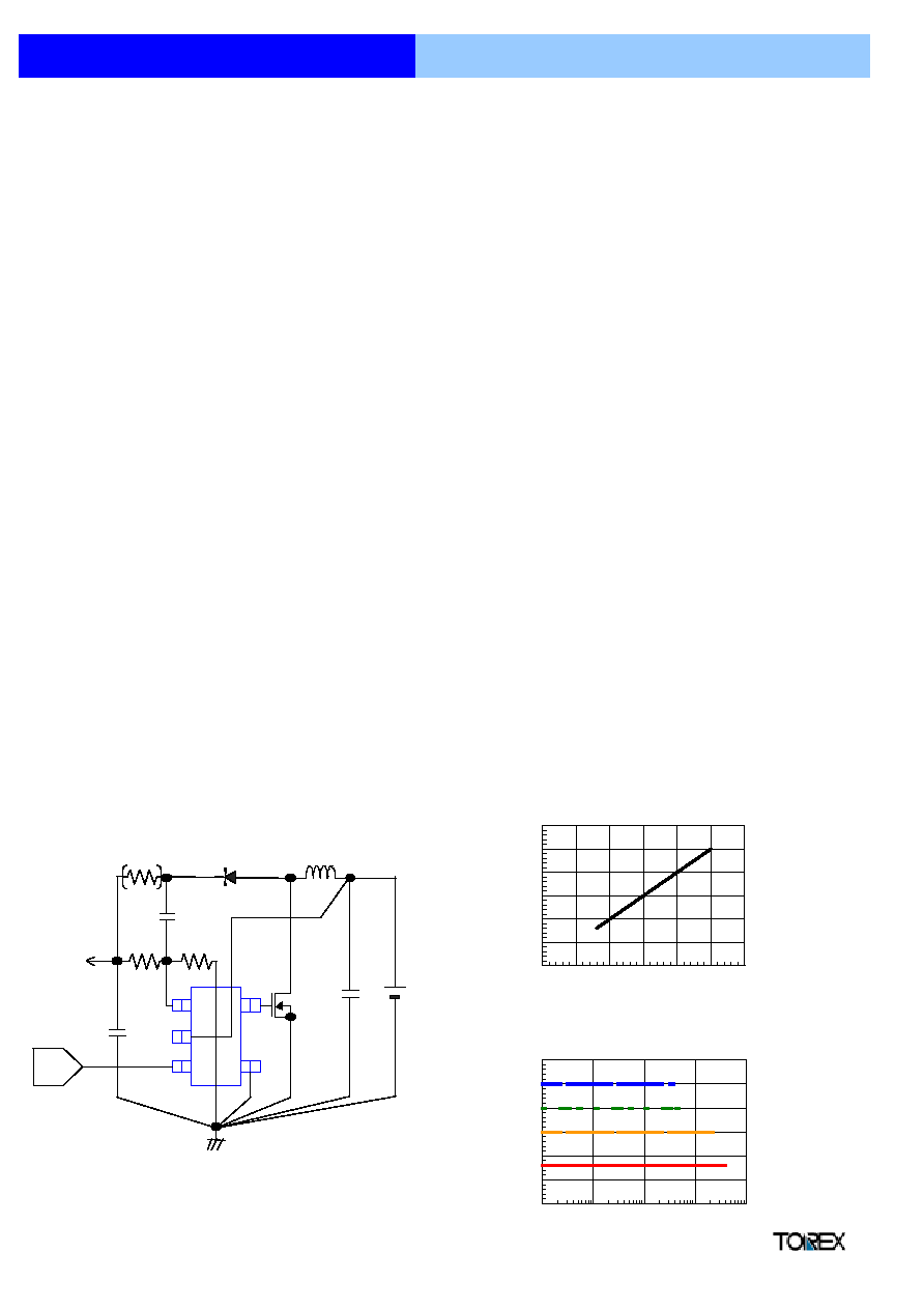
TYPICAL APPLICATION CIRCUIT
"
TYPICAL APPLICATION PERFORMANCE
1
PWM Control, PWM/PFM Switching Control,
Step-up DC/DC Converters
Externally Applied Reference Voltage (Vref)
XC9106 / 07 Series
(VIN=3.3V, VOUT=20V, when peripheral
components are used as in the circuits below .)
* RSENSE is of no use in light load (uncontinuous mode) applications such
as a small LCD, even using ceramic capacitor.
0
5
10
15
20
25
30
0.0
0.5
1.0
1.5
2.0
2.5
3.0
Vref (V)
V
OUT
(V
)
0
5
10
15
20
25
30
0.1
1
10
100
1000
I
OUT
(mA)
V
OUT
(V
)
2.0V
Vref=0.8V
1.5V
2.5V
Circuit as left
V
DD
=V
IN
=3.3V, I
OUT
=30mA
XC9107D003MR
XC9107D003MR
Circuit as left
V
DD
=V
IN
=3.3V
L : 10
µ
H
SD : MA737
CFB : 27pF
Nch Power
MOS FET
2SK2159
V
IN
= 3.3V
RFB2 :
30k
RFB1 :
270k
V
OUT
= 8V~25V
I
OUT
= 30mA
D/A converter
Ceramic CL :
10
µ
F
CE/Vref
CIN
RSENSE : 100m
for Ceramic CL
0.8V~2.5V
3
2
1
5
4
*
The XC9106 / 07 series are step-up DC/DC controller ICs
with an externally applied reference voltage (Vref).
Output voltage will be set with external resistors (RFB1 and 2)
and Vref value. The series make it easy to control output
voltage externally and are suited to software applications that
need to vary voltage, such as LCD power supply for PDA.
Output will be stable no matter which load capacitors are
used but if a low ESR capacitor is used, RSENSE of about
0.1
will be required and phase compensation will be
achieved. This makes the use of ceramic capacitors much
easier, and allows for lower output ripple and reduced PCB
area requirements. Tantalum and electrolytic capacitors can
also be used, in which case, RSENSE becomes
unnecessary.
Oscillation frequencies of high clock, low ripple 300kHz and
low supply current 100kHz are available.
The XC9107 series are PWM/PFM automatic switching
controlled. Control switches from PWM to PFM during light
loads with the XC9107 and the series is highly efficient from
light loads to large output currents. By bringing the whole
circuit down while the series is in the stand-by mode
(CE/PWM pin : low), supply current can be reduced to less
than 1.0
µ
A.
Semiconductor Ltd.
Preliminary
"
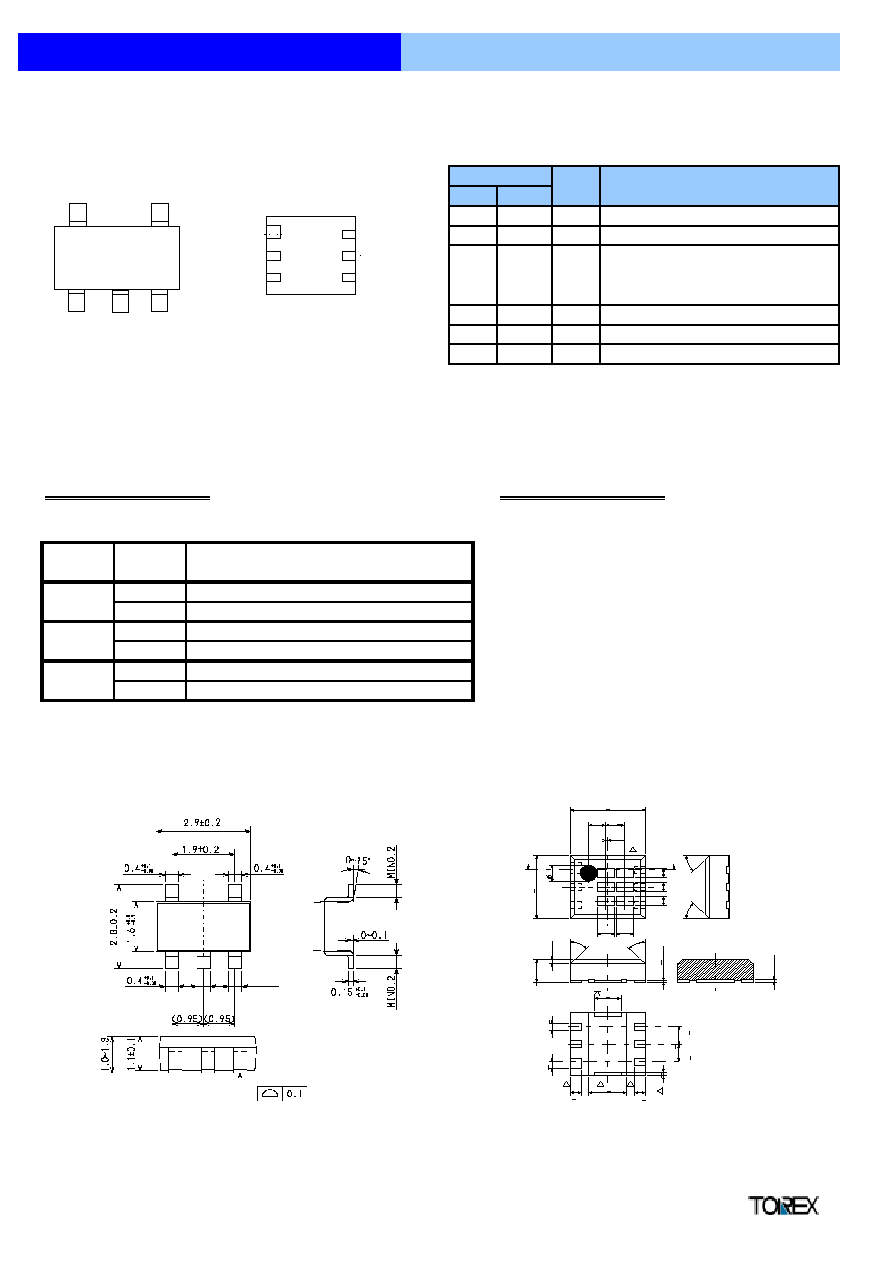
PIN CONFIGURATION
"
PIN ASSIGNMENT
"
ORDERING INFORMATION
XC9107 Series: PWM/PFM automatic switching control
XC9106 Series: PWM Control
(Ordering information is the same as XC9106 Series)
Reference Voltage (apply external)
Fixed : 00
Oscillation Frequency:
300kHz
100kHz
Package:
SOT-25 (1 reel = 3000 pcs.)
USP-6B (1 reel = 3000 pcs.)
Embossed Tape:
Standard Feed
Reverse Feed
"
PACKAGING INFORMATION
$
SOT-25 (SOT-23-5)
$
USP-6B
2
Externally Applied Reference Voltage (Vref)
XC9106 / 07 Series
PWM Control, PWM/PFM Switching Control,
Step-up DC/DC Converters
FUNCTION
Ground
GND
FB
VDD
R
L
5
M
1
4
D
Supply Voltage
NC
No Connection
3
5
PIN
NAME
XC9107D
12345
Output Resistor Connection
External Transistor Connection
EXT
2
6
2
SOT-25 USP-6B
XC9106D
12345
-
5
3
4
4
12
Serves as both Chip Enable pin and
Reference Voltage Apply pin.
CE/
Vref
3
3
1
PIN NUMBER
1
SOT-25
(TOP VIEW)
1
2
3
4
5
6
5
4
1
2
3
USP-6B
(TOP VIEW)
6
5
4
1
2
3
A
'
A
AAA
A
A
A
1
.
4
5
6
3
2
1
0
1
1
1
1
1
2.0 + 0.15
(0.45) 0.5+0.1
(0.05)
(0.45) (0.45)
45
O
45
O
1.
8+0.
15
(0
.2
7
)
(
0
.
27)
(0
.
2
7
)
(
0
.
4
5
)
45
O
45
O
(0
.1
2
5
)
(0
.6
5
)
0.
005
+0.
0
02
(0
.
0
5
)
-0
.
0
0
5
+0
.
0
1
-0
.
0
5
+0
.
1
5
0.7+0.03
5-
0.
2+0.
05
0.
5+0.
1
1.
6
+
0.
15
0.
5+0.
1
0.
1+0.
03
0.
2+0.
05
1.0+0.1
0.25+0.1
0.25+0.1
Semiconductor Ltd.
Preliminary
"
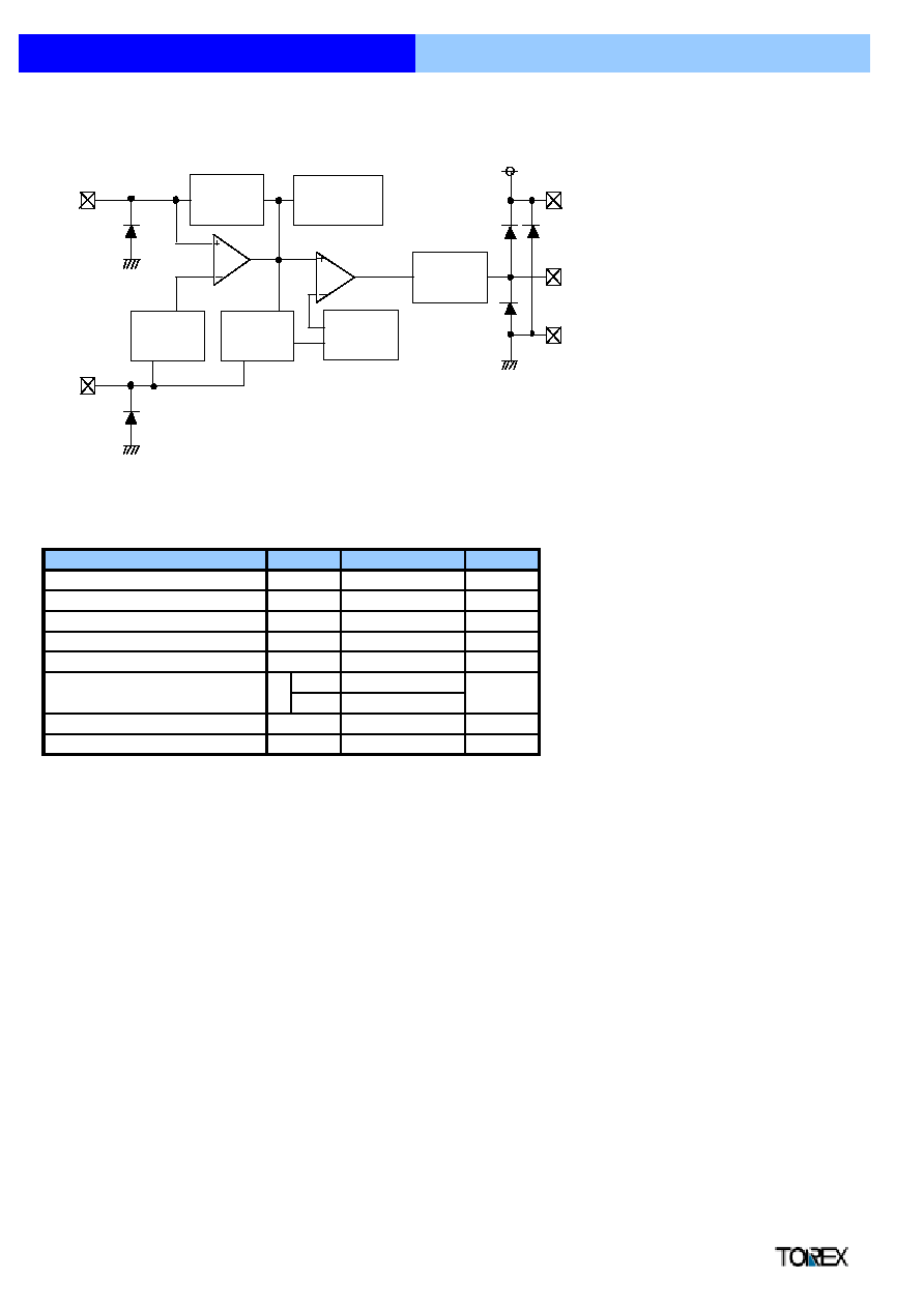
BLOCK DIAGRAM
"
ABSOLUTE MAXIMUM RATINGS
Ta = 25
O
C
3
XC9106 / 07 Series
PWM Control, PWM/PFM Switching Control,
Step-up DC/DC Converters
Externally Applied Reference Voltage (Vref)
mW
O
C
Storage Temperature
RATINGS
UNITS
V
V
-0.3 ~ 12.0
-0.3 ~ 12.0
SOT-25
USP-6B
-0.3 ~ 12.0
V
Tstg
O
C
-55 ~ +125
VDD
VFB
VCE / Vref
-0.3 ~ VDD + 0.3
mA
Topr
VEXT
IEXT/
±100
150
100
-40 ~ +85
V
Pd
SYMBOL
EXT pin Current
Power Dissipation
Operating Ambient Temperature
PARAMETER
VDD pin Voltage
FB pin Voltage
CE / Vref pin Voltage
EXT pin Voltage
Ramp Wave
Generator,
OSC
Current
Ripple Detect
and FB
PWM/PFM
Controller
Phase
Compensation
Vref with
Soft Start,
CE
Buffer,
Driver
Error Amp.
PWM
Comparator
FB
VDD
EXT
GND
CE / Vref
FB, CE : CMOS INPUT
EXT : CMOS OUTPUT
Semiconductor Ltd.

Preliminary
"
ELECTRICAL CHARACTERISTICS
XC9106D001MR, XC9107D001MR
(FOSC=100 (kHz)
Ta=25
O
C
*1
*1
Test Conditions: Unless otherwise stated, CL: ceramic, recommended MOS FET should be connected.
VDD =
(V)
!
Vref =
(V) ,
RFB1, 2 x 10
VIN =
(V)
!
IOUT =
(mA)
Notes 1* :
4
XC9106 / 07 Series
V
1
3
V
-
PWM Control, PWM/PFM Switching Control,
Step-up DC/DC Converters
Externally Applied Reference Voltage (Vref)
No external connections
Although the IC starts step-up operations from a VDD of 0.8V, the output voltage and oscillation frequency are stabilized at
VDD
1.8V or (Vref applied voltage + 0.7V). Therefore, a VDD of more than 1.8V or (Vref applied voltage + 0.7V) is recommended when VDD is
supplied from VIN or other power sources.
V
CIRCUIT
-
8.820
9.000
9.180
0.8
2.5
UNITS
4
µ
A
4
V
3
V
4
V
5
14
19
µ
A
1.0
µ
A
1
%
4
%
4
1
KHz
PARAMETER
Output Voltage
Reference Voltage Range
Operation Start Voltage
Power Supply Voltage Range
PFM Duty Ratio
FOSC
MAXDTY
PFMDTY
Oscillation Frequency
FB Control Voltage
VFB
Same as IDD1
Maximum Duty Ratio
Same as IDD1
Oscillation Start Voltage
VST2
CE/Vref=0.9V, Voltage applied, FB=0V
VST1
Recommended Circuit using 2SD1628, IOUT=1.0mA
Supply Current 2
Operation Holding Voltage
Supply Current 1
VDD
Vref = 0.9V
VDD as shown right or (Vref applied voltage+0.7V)
Efficiency
Recommended Circuit using 2SD1628, IOUT=1.0mA
Same as VST2, VDD=3.300V
ISTB
VHLD
IDD1
IDD2
Same as IDD1, CE/Vref=0V
Same as IDD1, FB=1.2V
Stand-by Current
V
No Load (XC9106 series)
Recommended Circuit using XP161A1355
EFFI
%
20
28
36
85
1
Soft-start Time
Vref=0.9V
mS
TSS
5.0
10.0
20.0
5
CE "Low" Voltage
VCEL
Same as IDD1
CE "High" Voltage
VCEH
Same as IDD1
0.20
24
36
5
V
4
4
EXT "Low" ON Resistance
REXTL
Same as IDD1, VEXT=VOUT-0.4V
EXT "High" ON Resistance
REXTH
Same as IDD1, VEXT=0.4V
16
24
CE "Low" Current
ICEL
Same as IDD2, CE=0.8V
Same as IDD2, CE=0V
-1.0
µ
A
µ
A
5
0.0
Same as IDD2, FB=VDD
5
-0.1
0.1
5
FB "High" Current
IFBH
µ
A
Same as IDD2, FB=1.0V
IFBL
-0.1
1.8
CONDITIONS
Vref = 0.9V
SYMBOL
VOUT
Vref
MIN.
TYP.
MAX.
0.784
0.800
0.816
0.8
10.0
0.9
0.7
29
41
75
81
87
85
100
115
0.65
FB "Low" Current
0.09
50
3.30
3.30
Vref = 0.9V
Vref = 2.5V
0.882
0.900
0.918
2.450
2.500
2.550
4
V
CE "High" Current
ICEH
Same as IDD2, CE=2.5V
0.0
2.5
µ
A
5
Semiconductor Ltd.
Preliminary
"
ELECTRICAL CHARACTERISTICS
XC9106D003MR, XC9107D003MR
(FOSC=300 (kHz)
Ta=25
O
C
*1
*1
Test Conditions: Unless otherwise stated, CL: ceramic, recommended MOS FET should be connected.
VDD =
(V)
!
Vref =
(V) ,
RFB1, 2 x 10
VIN =
(V)
!
IOUT =
(mA)
Notes 1* :
"
TYPICAL APPLICATION CIRCUIT
5
PWM Control, PWM/PFM Switching Control,
Step-up DC/DC Converters
Externally Applied Reference Voltage (Vref)
Although the IC starts step-up operations from a VDD of 0.8V, the output voltage and oscillation frequency are stabilized at
VDD
1.8V or (Vref applied voltage + 0.7V). Therefore, a VDD of more than 1.8V or (Vref applied voltage + 0.7V) is recommended when VDD is
supplied from VIN or other power sources.
XC9106 / 07 Series
PARAMETER
SYMBOL
CONDITIONS
MIN.
TYP.
MAX.
UNITS CIRCUIT
Output Voltage
VOUT
Vref = 0.9V
8.820
9.000
9.180
V
1
Reference Voltage Range
Vref
0.8
2.5
V
-
Vref = 0.8V
0.784
FB Control Voltage
VFB
Vref = 0.9V
0.882
0.800
0.816
V
4
Power Supply Voltage Range
VDD
VDD as shown right or (Vref applied voltage + 0.7V)
1.8
10.0
V
-
Operation Start Voltage
VST1
Recommended Circuit using 2SD1628, IOUT=1.0mA
0.9
V
3
Oscillation Start Voltage
VST2
No external connections
CE/Vref=0.9V, Voltage applied, FB=0V
0.8
V
4
Operation Holding Voltage
VHLD
Recommended Circuit using 2SD1628, IOUT=1.0mA
0.7
V
3
Supply Current 1
IDD1
Same as VST2, VDD=3.300V
62
88
µ
A
4
Supply Current 2
IDD2
Same as IDD1, FB=1.2V
16
22
µ
A
4
Stand-by Current
ISTB
Same as IDD1, CE/Vref=0V
1.0
µ
A
5
Oscillation Frequency
FOSC
Same as IDD1
255
300
345
KHz
4
Maximum Duty Ratio
MAXDTY Same as IDD1
75
81
87
%
4
PFM Duty Ratio
PFMDTY No Load (XC9106 series)
24
32
40
%
1
Efficiency
EFFI
Recommended Circuit using XP161A1355
85
%
1
Soft-start Time
TSS
Vref=0.9V
5.0
10.0
20.0
mS
1
CE "High" Voltage
VCEH
Same as IDD1
0.65
V
5
CE "Low" Voltage
VCEL
Same as IDD1
0.20
V
5
EXT "High" ON Resistance
REXTH
Same as IDD1, VEXT=VOUT-0.4V
24
36
4
EXT "Low" ON Resistance
REXTL
Same as IDD1, VEXT=0.4V
16
24
4
Same as IDD2, CE=0.8V
-1.0
CE "High" Current
ICEH
Same as IDD2, CE=2.5V
0.0
CE "Low" Current
ICEL
Same as IDD2, CE=0V
-0.1
µ
A
5
FB "High" Current
IFBH
Same as IDD2, FB=VDD
0.1
µ
A
5
FB "Low" Current
IFBL
Same as IDD2, FB=1.0V
-0.1
µ
A
5
3.30
0.09
3.30
50
When obtaining VDD from a source other than VOUT, please insert a
capacitor CDD between the VDD pin and the GND pin in order to
provide stabler operations.
Please wire CL & CIN between the VOUT/VDD pin and the GND pin.
Strengthen the wiring sufficiently. When using a capacitor other than
ceramic or low ESR at CL, please take away RSENSE and short.
Insert Rb and CB when using a
bipolar NPN Transistor.
0.900
0.918
Vref = 2.5V
2.450
2.500
2.500
2.5
µ
A
5
0.0
V
OUT
Nch Power
MOS FET
RSENSE
L
V
IN
SD
R
FB1
R
FB2
C
FB
CE/Vref
1
5
4
3
2
CL
Rb
Cb
Semiconductor Ltd.
Preliminary
"
OPERATIONAL DESCRIPTION
<Error Amp.>
<OSC Generator>
<Ramp Wave Generator>
The Ramp Wave Generator generates a saw-tooth waveform based on outputs from the OSC Generator.
<PWM Comparator>
<PWM/PFM Controler>
<Vref 1 with Soft Start>
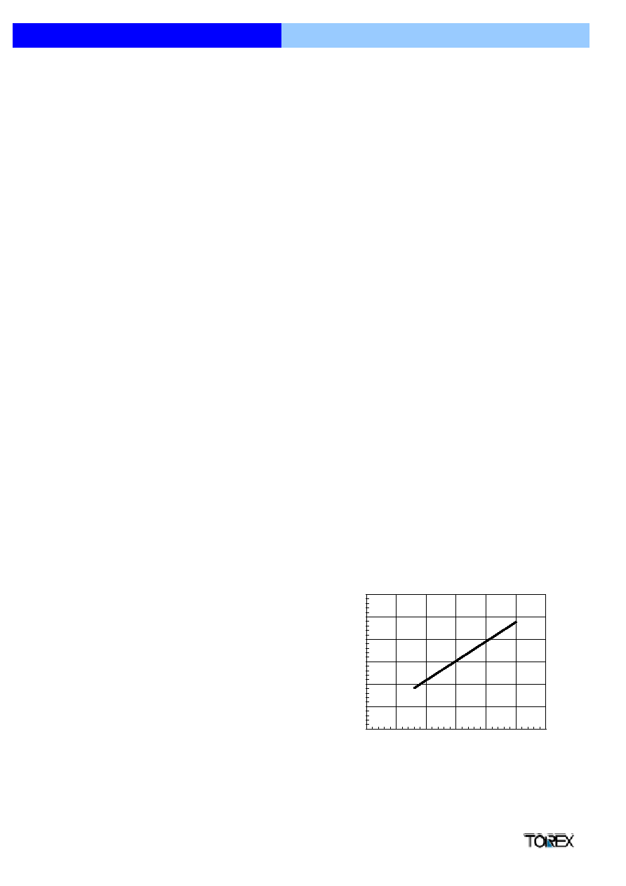
TSS = 8.65 x Vref + 2.21
[Example Computation]
Vref = 0.9V, TSS = 8.65 x 0.9 + 2.21 = 10.0 ms
<Enable Function>
6
XC9106 / 07 Series
PWM Control, PWM/PFM Switching Control,
Step-up DC/DC Converters
This function controls the operation and shutdown of the IC. When the voltage of the CE pin drops to 0.2V or less, disable mode will be entered, the
IC's operations will stop and the EXT pin will be kept at a low level (the external N-type MOSFET will be OFF) . When the IC is in a state of chip
disable, current consumption will be no more than 1.0
µ
A.
When the CE pin's voltage rises to 0.65V or more, enable mode will be entered and operations will recommence. The CE pin also doubles with
reference voltage in the XC9106/9107 series, and the range of reference voltage can be varied externally from 0.8V to 2.5V.
The XC9106/9107 series alters soft start times by the setting value of reference voltage in order to protect against voltage overshoot and also to
protect against inrush current. Please determine soft start time by the formula equation.
Error Amplifier is designed to monitor the output voltage, comparing the feedback voltage (FB) with the reference voltage Vref. In response to
feedback of a voltage lower than the reference voltage Vref, the output voltage of the error amp. decreases.
This circuit generates the internal reference clock.
The PWM Comparator compares outputs from the Error Amp. and saw-tooth waveform. When the voltage from the Error Amp's output is low, the
external switch will be set to ON.
This circuit generates PFM pulses.
The PWM/PFM automatic switching mode switches between PWM and PFM automatically depending on the load. PWM/PFM control turns into
PFM control when threshold voltage becomes lower than voltage of error amps. Noise is easily reduced with PWM control since the switching
frequency is fixed. Because of the function, control suited to the application can easily be selected. The series suitable for noise sensitive portable
audio equipment as PWM control can suppress noise during operation and PWM/PFM switching control can reduce consumption current during light
loads in stand-by.
The reference voltage of the XC9106/9107 series is adjusted and fixed by external applied voltage. (For output voltage settings, please refer to the
output voltage setting on page 7.)
To protect against inrush current, when the power is switched on, and also to protect against voltage overshoot, soft-start time is set internally to
10ms. It should be noted, however, that this circuit does not protect the load capacitor (CL) from inrush current. With the Vref voltage limited, and
depending upon the input to error amp, the operation maintains a balance between the two inputs of error amps and controls the EXT pin's ON time
so that it doesn't increase more than is necessary.
The XC9106 / 07 series are reference voltage (Vref) apply external step-up DC/DC Controler ICs. Output voltage will be set with external resistors
(RFB1 and 2) and Vref value. The series make it easy to control output voltage externally and are suited to software applications that need to vary
voltage such as LCD power supply for PDA.
Externally Applied Reference Voltage (Vref)
XC9106 / XC9107D xxx MR
0
5
10
15
20
25
30
0.0
0.5
1.0
1.5
2.0
2.5
3.0
Reference Voltage Vref (V)
Soft Start Time : TSS (ms)
Semiconductor Ltd.
Semiconductor Ltd.

Preliminary
"
FUNCTIONAL SETTINGS
< Output Voltage Setting>
VOUT = Vref applied voltage x (RFB1 + RFB2) / RFB2
fzfb = 30kHz (L=10
µ
H)
RFB1 : 270k
RFB2 : 30k
fzfb = 20kHz (L=22
µ
H)
CFB :
20pF
(fzfb = 30kHz, L = 10
µ
H)
fzfb = 10kHz (L=47
µ
H)
27pF
(fzfb = 20kHz, L = 22
µ
H)
56pF
(fzfb = 10kHz, L = 47
µ
H)
< The use of ceramic capacitor CL >
"
RECOMMENDED COMPONENTS
Tr:
*When a MOSFET is used :
*When a NPN Tr. Is used :
2SK2159 (NEC N-Channel Power MOSFET)
2SD1628 (Sanyo)
Rb
: 500
(adjust with Tr's HFE or load)
Cb
: 2200pF (ceramic type)
Cb
1 / (2
◊
Rb
◊
FOSC
◊
0.7)
SD:
MA2Q737 (Schottky Diode type, MATSUSHITA)
L, CL :
Adjust as below according to the condition and peripheral components
When Ceramic capacitor is used :
L :
22
µ
H (SUMIDA CDRH5D28, FOSC = 100kHz)
10
µ
H (SUMIDA CDRH5D18, FOSC = 300kHz)
CL :
10V 10
µ
F (Ceramic capacitor, LMK325BJ106ML, TAIYOYUDEN)
Use the formula below when step-up ratio and output current is large.
CL = (CL standard value)
◊
(IOUT(mA) / 300mA
◊
VOUT / VIN)
RSENSE : 100m
(FOSC = 300kHz)
50m
(FOSC = 100kHz)
When Tantalum capacitor is used :
L:
22
µ
H (SUMIDA CDRH5D28, FOSC = 300kHz)
47
µ
H (SUMIDA CDRH5D28, FOSC = 100kHz)
Except when IOUT(mA) / 100mA
◊
VOUT / VIN > 2
22
µ
H
CL:
16V 47
µ
F (tantalum type NIPPONCHEMI 16MCE476MD2)
Use the formula below when step-up ratio and output current is large.
CL = (CL standard value)
◊
(IOUT(mA) / 300mA
◊
VOUT / VIN)
RSENSE:
Not required, but short out the wire.
When AL Electrolytic capacitor is used :
L:
22
µ
H (SUMIDA CDRH5D28, FOSC = 300kHz)
47
µ
H (SUMIDA CDRH5D28, FOSC = 100kHz)
Except when IOUT(mA) / 100mA
◊
VOUT / VIN > 2
22
µ
H
CL:
16V 100
µ
F (AL electrolytic type) + 10V 2.2
µ
F (ceramic type)
Strengthen appropriately when step-up ratio and output current is large.
RSENSE:
Not required, but short out the wire.
CFB:
Set up so that fzfb = 100kHz.
7
The circuit of the XC9106/9107 series is organized by a specialized circuit which reenacts negative feedback of both voltage and current. Also by
insertion of approximately 100m
of a low and inexpensive sense resistor as current sense, a high degree of stability is possible even using a
ceramic capacitor, a condition which used to be difficult to achieve. Compared to a tantalum condenser, because the series can be operated in a
very small capacity, it is suited to use of the ceramic capacitor which is cheap and small.
Note* : With direct voltages over 4.5V, use the
XP161A11A1PR.
XC9106 / 07 Series
PWM Control, PWM/PFM Switching Control,
Step-up DC/DC Converters
Externally Applied Reference Voltage (Vref)
The value of CFB1, speed-up capacitor for phase compensation, should result in fzfb = 1/(2
◊
CFB
◊
RFB1) equal to 5 to 30kHz. Adjustments are
required depending on the application, value of inductance (L), and value of load capacity (CL).
Output voltage can be set by adding external split resistors. Output voltage is determined by the following equation, based on the values of RFB1
and RFB2. The sum of RFB1 and RFB2 should normally be 2 M
or less. The range of reference voltage of the series can be varied externally
from 0.8V to 2.5V.
Semiconductor Ltd.
Preliminary
"
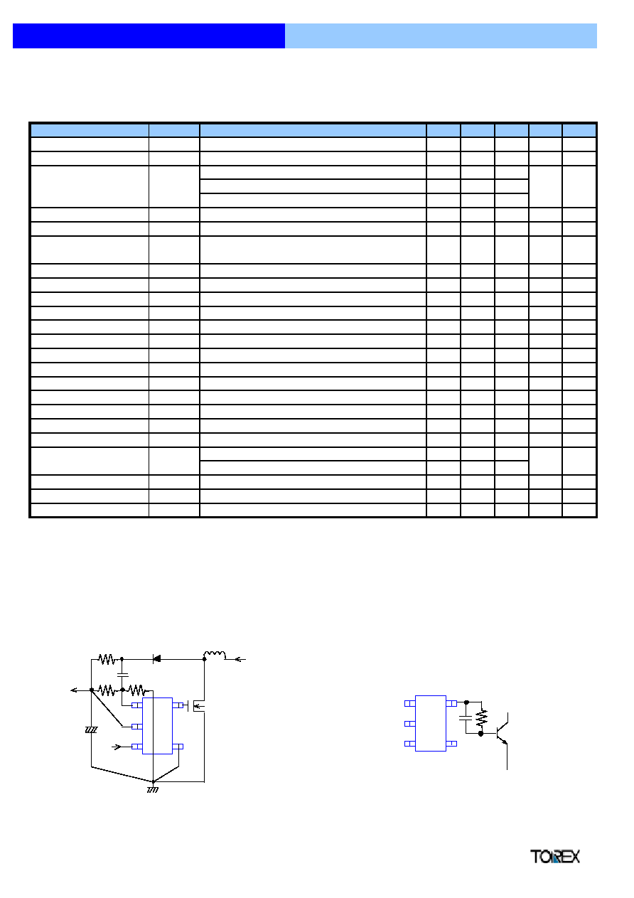
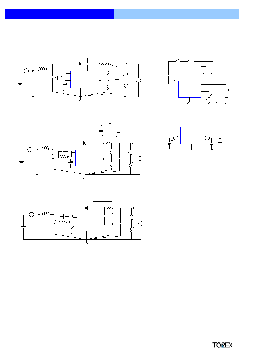
TEST CIRCUITS
Circuit
1
Circuit
4
Circuit
2
Circuit
5
Circuit
3
8
PWM Control, PWM/PFM Switching Control,
Step-up DC/DC Converters
Externally Applied Reference Voltage (Vref)
XC9106 / 07 Series
V
IN
L
SD
Tr
EXT
C
IN
GND
V
DD
FB
CE
CL
CFB
R
FB1
R
FB2
A
RL
V
OUT
V
A
OSC
R
SENSE
V
DD
FB
EXT
CE
GND
OSC
A
RP
C
DD
CP
L
SD
Tr
EXT
C
IN
GND
V
DD
FB
CE
CL
C
FB
RFB1
RFB2
R
SENSE
CB
OSC
V
IN
A
RB
A
RL
V
A
C
E
V
DD
FB
EXT
CE
GND
A
A
A
L
SD
Tr
EXT
C
IN
GND
V
DD
FB
CE
CL
C
FB
RFB1
RFB2
R
SENSE
CB
OSC
V
IN
A
RB
RL
V
A
Semiconductor Ltd.