 | –≠–ª–µ–∫—Ç—Ä–æ–Ω–Ω—ã–π –∫–æ–º–ø–æ–Ω–µ–Ω—Ç: XC9502 | –°–∫–∞—á–∞—Ç—å:  PDF PDF  ZIP ZIP |
Mar, 14 2003 Ver. 2
!
Applications
"
2ch DC/DC Controller (Step-up + Step-down)
#
PDAs
"
Input Voltage Range 0.9V ~ 10.0V
#
Palm Top Computers
"
Output Voltage Externally Set-Up
#
Portable Audio Systems
"
Switching Frequency 180kHz (±15%)
#
Various Multi-Function Power Supplies
"
Maximum Duty Cycle
Step-up 80% (Typ.)
Step-down 100%
"
PWM, PWM/PFM Switching Control
!
Features
"
High Efficiency
Step-up 85% (Typ.)
2ch DC/DC Controller
Step-down 92% (Typ.)
Output 1 : Step-up DC/DC Controller
"
Small MSOP-10 package
Output 2 : Step-down DC/DC Controller
Power Supply Voltage Range : 2.0V ~ 10V
Output Voltage Range
Output 1 (Step-up) : 1.5V ~ 30.0V
!
General Description
Output 2 (Step-down) : 0.9V ~ 6.0V
Oscillation Frequency
: 180kHz
±
15%
(300kHz, 500kHz custom)
Output Current
Output 1
Output 2
Stand-By Function
: 3.0
µ
A (MAX.)
Package
: MSOP-10
Soft-Start Time
: 10 ms (internally set)
!
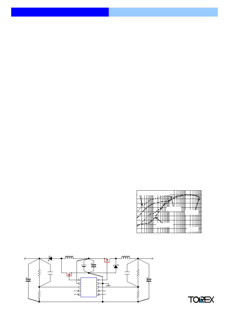
Typical Performance Characteristics
!
Typical Application Circuit
XC9502B092A Input :
2 cell, VOUT
1
: 3.3V, VOUT
2
: 1.8V
: more than 1000mA (VIN=3.3V, VOUT=1.8V)
: more than 300mA
(V
IN
=1.8V, V
OUT
=3.3V)
Noise is easily reduced with PWM control since the frequency
is fixed. The series gives freedom of control selection so that
control suited to the application can be selected. Soft-start
time is internally set to 10msec (Output 1) and offers protection
against in-rush currents when the power is switched. This also
prevents voltage overshoot.
Can be set freely with 0.9V
(
±
2.0%) of reference voltage supply
and external components.
Can be set freely with 0.9V
(
±
2.0%) of reference voltage supply
and external components.
XC9502 Series
2ch. Step-up / down DC/DC Controller ICs
The XC9502 series are PWM controlled, PWM/PFM automatic
switching controlled, multi-functional, 2 channel step-up and
down DC/DC controller ICs. With 0.9V of standard voltage
supply internal, and using externally connected components,
the output 1 voltage (step-up DC/DC controller) can be set
freely within a range of 1.5V to 30V. Since the output 2 (step-
down DC/DC controller) has a built-in 0.9V reference voltage
(accuracy ±2%), 0.9V to 6.0V can be set using external
components. With a 180kHz frequency, the size of the
external components can be reduced. Switching frequencies
of 300kHz & 500kHz are also available as custom-designed
products.
The control of the XC9502 series can be switched between
PWM control and PWM/PFM automatic switching control using
external signals. Control switches from PWM to PFM during
light loads when automatic switching is selected and the series
is highly efficient from light loads through to large output
currents.
Tr2:Nch
MOSFET
:XP161A1355P
L1:22
µ
H
CDRH5D28
Tr2:Pch
MOSFET
XP162A12A6P
C
IN
:47
µ
F
VIN
=2.0V
~3.0V
SD2
:MA2Q737
SD1
:MA2Q737
RFB11
:200k
CFB1
:62pF
RFB12
:75k
V
OUT
1:3.3V
1 EXT1
2 VDD
3 FB1
FB2 8
GND 9
EXT2/ 10
4 PWM1 PWM2 7
5 EN1
EN2 6
CL1
:47
µ
FX2
CL2
:47
µ
FX2
V
PWM1
V
PWM2
V
NE2
V
NE1
L2:22
µ
H
CDRH5D28
V
OUT
2:1.8V
RFB21
:220k
RFB22
:220k
CFB2
:62pF
0
10
20
30
40
50
60
70
80
90
100
0.1
1
10
100
1000
Output Current 1,2 I
OUT1,2
(mA)
E
f
f
i
c
i
enc
y
1,
2 E
FFI
1,
2 (%
)
V
IN
=2.7V
V
OUT2
:1.8V
PWM Control
PWM/PFM Switching Control
L1=15
µ
H,L2=22
µ
H(CDRH5D28),C
L1,
C
L2
=92
µ
F(Tantalum)
SD1,SD2:CMS02, Tr1:XP161A1355P,Tr2:XP162A12A6P
XC9502B093A (300kHz,VOUT1:3.3V,VOUT2:1.8V)
V
OUT1
:3.3V
1
!
Pin Configuration
!
Pin Assignment
!
Ordering Information
XC9502
123456
FB Voltage
0.9V
Embossed Tape
Embossed Tape
6
1
2
3
4
DESCRIPTION
DESIGNATOR
5
9
SYMBOL
L
Package
R
Standard Feed
Reverse Feed
MSOP-10
5
Switching Frequency
Standard (10 Pin)
PIN NAME
FUNCTIONS
2
3
300kHz (custom)
500kHz (custom)
1
2
5
EN1
Channel 1 : Enable Pin <Connected to Ground when Output 1 is in stand-by mode.
Connected to VDD when Output 1 is active. EXT1 is low when in stand-by mode.>
6
EN2
Channel 2 : Enable Pin <Connected to Ground when Output 2 is in stand-by mode.
Connected to VDD when Output 2 is active. EXT2/ is high when in stand-by mode.>
XC9502 Series
B
0
A
PIN NUMBER
3
Channel 1 : Output Voltage Monitor Feedback Pin <Threshold value : 0.9V. Output voltage
can be set freely by connecting split resistors between VOUT1 and Ground.>
4
PWM1
Channel 1 : PWM/PFM Switching Pin <Control Output 1. PWM control when connected to
V
DD
, PWM / PFM auto switching when connected to Ground. >
2ch. Step-up / down DC/DC Controller ICs
180kHz
EXT 1
Channel 1: External Transistor Drive Pin <Connected to Nch Power MOSFET Gate>
V
DD
Supply Voltage
FB1
7
PWM2
Channel 2 : PWM/PFM Switching Pin <Control Output 2. PWM control when connected to
VDD, PWM / PFM auto switching when connected to Ground.>
8
FB2
Channel 2 : Output Voltage Monitor Feedback Pin <Threshold value : 0.9V. Output voltage
can be set freely by connecting split resistors between VOUT2 and Ground.>
9
GND
Ground
10
EXT2/
Channel 2 : External Transistor Drive Pin <Connected to Pch Power MOSFET Gate>
1 EXT1
2 VDD
3 FB1
FB2 8
GND 9
EXT2 10
4 PWM1
PWM2 7
5 EN1
EN2 6
MSOP-10
(TOP VIEW)
2

!
Absolute Maximum Ratings
Ta=25
O
C
* Voltage goes to Ground.
!
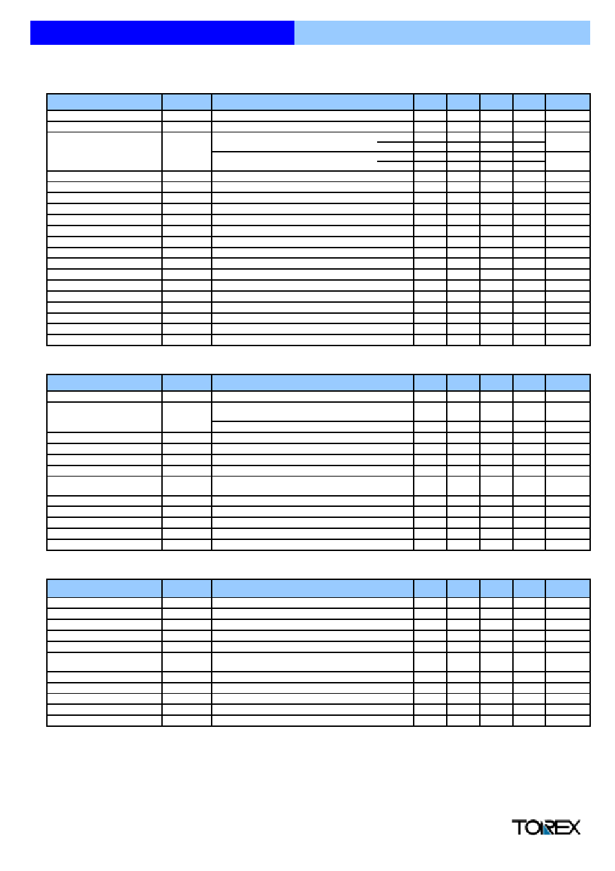
Block Diagram
Storage Temperature
mW
I
EXT
± 100
mA
Pd
150
EXT1, 2 Pin Current
Power Dissipation
FB1, 2 Pin Voltage
- 0.3 ~ 12
V
V
V
EN
- 0.3 ~ 12
V
- 0.3 ~ 12
V
V
EXT
- 0.3 ~ V
DD
+ 0.3
EN1, 2 Pin Voltage
PWM1,2 Pin Voltage
EXT1, 2 Pin Voltage
V
PWM
V
DD
- 0.3 ~ 12
V
SYMBOL
RATINGS
UNITS
PARAMETER
XC9502 Series
2ch. Step-up / down DC/DC Controller ICs
V
DD
Pin Voltage
V
FB
Tstg
O
C
- 55 ~ + 125
O
C
Topr
- 40 ~ + 85
Operating Ambient Temperature
PWM1
+
-
FB1
VDD
EXT1
Vref1 = 0.9V
with Soft Start1,
EN1
+
-
PWM/PFM
Controller 1
Vref2 = 0.9V
with Soft Start 1,
EN2
+
-
PWM/PFM
Controller 2
FB2
GND
EXT2
OSC
Generator
Ramp Wave
Generator 1
Ramp Wave
Generator 2
Error
Amp2
Error
Amp1
PWM
Comparator2
PW
M
Comparator1
EN1
PWM2
EN2
EN1 to
internal circuit
EN2 to
internal circuit
-
+
3
!
Electrical Characteristics
XC9502B092
Common Characteristics
(FOSC=180kHz)
Ta=25
O
C
VOUT1
VOUT2
VOUT1
VOUT2
Unless otherwise stated, VDD=3.0V, PWM1,2=3.0V, EN1, 2 =3.0V
Output 1 Characteristics
Step-up Controller
Ta=25
O
C
Using Tr: 2SD1628,
Unless otherwise stated, VDD=EN1=PWM1=3.0V, EN2=PWM2=GND, EXT2=OPEN, FB2=OPEN, VIN=1.8V
Output 2 Characteristics
Step-down Controller
Ta=25
O
C
Unless otherwise stated, VDD=EN2=PWM2=3.0V, PWM1=EN1=GND, EXT1=OPEN, FB1=OPEN, VIN=5.0V
Notes
1)
2)
3)
4)
IOUT2=250mA
%
MAXDTY2
100
-
-
Same as IDD1
%
MAX.
0.900
0.918
Efficiency1 (note 4)
EFFI1
IOUT=130mA
-
N-ch MOSFET:XP161A1355P
Oscillation Start-up Voltage1
VST2-1
-
MIN.
0.882
-
IFBH
FB1, 2=3.0V
FB1, 2=1.0V
FB1,2 "Low" Current
-
60
130
FB1=1.0V, FB2=0V
Same as IDD2
-
-
0.900
Max. Input Voltage
VIN
10.0
-
V
1
Supply Current 1-4
-
PARAMETER
SYMBOL
CONDITIONS
µ
A
FB1, 2=1.0V
3.0
µ
A
Stand-by Current
ISTB
Same as IDD1, EN1=EN2=0V
UNITS
MIN.
PARAMETER
SYMBOL
CONDITIONS
3
Efficiency2 (note 4)
EFFI2
P-ch MOSFET : XP162A12A6P
8
92
-
-
%
8
8
V
8
Although the IC's step-up operations start from a VDD of 0.8V, the output voltage and switching frequency are stabilized at VDD
2.0V. Therefore, a VDD of more than 2.0V is recommended when VDD is supplied from VIN or other power sources.
V
TYP.
FB1 Voltage
VFB1
Soft-Start Time1
EXT1 "Low" ON Resistance
VDD=3.0V, VIN=1.5V, IOUT1=10mA
0.65
FB1=0V
-
2.0
-
PWM1,2 "Low" Current
IDD1-4
IPWML
FB1, 2=3.0V, PWM=0V
FB1, 2=0V
Supply Current 2
IDD2
Soft-Start Time2
PARAMETER
SYMBOL
MIN.
0.9
Supply Voltage (note 1)
VDD
VFBL
FB1,2 "High" Current
EN1=3.0V, EN2=0V, FB1=0V
PWM1,2 "High" Current
IPWMH
VPWMH2 No Load
EN2=0, EXT2=VDD-0.4V
EXT2 "Low" ON Resistance
REXTBL2 FB2=0V, EXT2=0.4V
EXT2 "High" ON Resistance
REXTBH2
Minimum Operation Voltage
5.0
-
6
%
10.0
30
38
-
6
47
22
28
30
PWM2 "Low" Voltage
VPWML2 No Load
-
PWM2 "High" Voltage
8
-
-
0.20
-
-
TSS2
VOUT2
◊
0.95V, EN2=0V
0.65V
VINmin
-
PFM Duty Ratio2
PFMDTY2 No Load, VPWM2=0V
Minimum Duty Ratio2
22
MINDTY2
MAX.
TYP.
120
85
-
60
130
0
2.0
-
%
-
VIN
-
60
-
VIN
10.0
CONDITIONS
2ch. Step-up / down DC/DC Controller ICs
TEST
CIRCUIT
MAX.
UNITS
-
TYP.
XC9502 Series
-
Output Voltage Range
(note 3)
VOUTSET
0.9
2.0
Supply Current 1-1
IDD1-1
Supply Current 1
IDD1
VIN
0.9V, IOUT1, 2=1mA
VDD=VOUT1
110
µ
A
Supply Current 1-2
IDD1-2
EN2=3.0V, EN1=0V, FB2=0V
-
50
160
µ
A
Supply Current 1-3
IDD1-3
FB1=0V, FB2=1.0V
-
70
-
1.0
180
207
Switching Frequency
FOSC
Same as IDD1
153
-
-
V
EN1,2 "High" Voltage
VENH
FB1,2=0V
0.65
-
0.20
V
EN1,2 "Low" Voltage
VENL
FB1,2=0V
-
-
0.50
µ
A
EN1,2 "High" Current
IENH
EN1,2=3.0V
-
-
-0.50
µ
A
EN1,2 "Low" Current
IENL
EN1,2=0V, FB1,2=3.0V
-
FB1, 2=3.0V, PWM=3.0V
-
0.918
-
0.50
-
-0.50
-0.50
-
0.50
-
V
V
Operation Start-up Voltage1
(note 2)
VST1-1
-
-
IOUT1=1.0mA, RFB11=200k
, RFB12=75k
VDD
VOUT1: IOUT1=1mA
0.9
%
80
85
-
2.0
0.8
-
28
47
20.0
10.0
30
38
-
0
FB2 Voltage
VFB2
VIN=3.0V, IOUT2=10mA
0.882
EXT1 "High" ON Resistance
REXTBL1
-
-
-
22
30
-
PWM1 "High" Voltage
VPWMH1
No Load, VPWM1=0V
22
Maximum Duty Ratio1
MAXDTY1 Same as IDD1
PFM Duty Ratio1
75
PFMDTY1
Minimum Duty Ratio1
MINDTY1
TSS1
VOUT1
◊
0.95V, EN1=0V
0.65V
5.0
REXTBH1 FB1=0, EXT1=VDD-0.4V
No Load
-
-
EN1=FB2=0V, EXT1=0.4V
No Load
0.65
%
V
VDD
2.0V, IOUT1, 2=1mA
VDD
VOUT1
V
µ
A
70
160
-
-
-
0.9
V
V
-
10.0
3
1
1
3
3
2
3
3
3
3
V
V
µ
A
µ
A
kHz
µ
A
UNITS
V
µ
A
µ
A
µ
A
5
5
V
mS
5
3
3
6
6
EFFI={ [ (Output voltage) x (Output current) ] / [ (Input voltage) x (Input Current) ] } x 100
-
Same as IDD2
0.20
V
PWM1 "Low" Voltage
VPWML1
Maximum Duty Ratio2
20.0
mS
7
TEST
CIRCUIT
V
TEST
CIRCUIT
%
5
Although the IC's switching operations start from a VIN of 0.9V, the IC's power supply pin (VDD) and output voltage monitor pin
(FB1) should be connected to VOUT1. With operations from VIN=0.9V, the 2nd channel's (output 2) EN2 pin should be set to chip
disable. Once ouput voltage VOUT1 is more than 2.0V, the EN2 pin should be set to chip enable.
Please be careful not to exceed the breakdown voltage level of the peripheral parts.
3
3
3
3
3
3
3
3
4
5
2
3
1
V
1
3
3
4
!
Electrical Characteristics
XC9502B093
Common Characteristics
(FOSC=300kHz)
Ta=25
O
C
VOUT1
VOUT2
VOUT1
VOUT2
Unless otherwise stated, VDD=3.0V, PWM1,2=3.0V, EN1, 2 =3.0V
Output 1 Characteristics
Step-up Controller
Ta=25
O
C
Using Tr: 2SD1628,
Unless otherwise stated, VDD=EN1=PWM1=3.0V, EN2=PWM2=GND, EXT2=OPEN, FB2=OPEN, VIN=1.8V
Output 2 Characteristics
Step-down Controller
Ta=25
O
C
Unless otherwise stated, VDD=EN2=PWM2=3.0V, PWM1=EN1=GND, EXT1=OPEN, FB1=OPEN, VIN=5.0V
Notes
1)
2)
3)
4)
Although the IC's step-up operations start from a VDD of 0.8V, the output voltage and switching frequency are stabilized at VDD
2.0V. Therefore, a VDD of more than 2.0V is recommended when VDD is supplied from VIN or other power sources.
Although the IC's switching operations start from a VIN of 0.9V, the IC's power supply pin (VDD) and output voltage monitor pin
(FB1) should be connected to VOUT1. With operations from VIN=0.9V, the 2nd channel's (output 2) EN2 pin should be set to chip
disable. Once ouput voltage VOUT1 is more than 2.0V, the EN2 pin should be set to chip enable.
Please be careful not to exceed the breakdown voltage level of the peripheral parts.
EFFI={ [ (Output voltage) x (Output current) ] / [ (Input voltage) x (Input Current) ] } x 100
-
0.20
V
8
PWM2 "Low" Voltage
VPWML2 No Load
-
-
-
V
8
PWM2 "High" Voltage
VPWMH2 No Load
0.7
22
30
6
EXT2 "Low" ON Resistance
REXTBL2 FB2=0V, EXT2=0.4V
-
28
47
6
EXT2 "High" ON Resistance
REXTBH2 EN2=0V, EXT2=VDD-0.4V
-
10.0
20.0
mS
8
Soft-Start Time2
TSS2
VOUT2
◊
0.95V, EN2=0V
0.65V
5.0
92
-
%
8
Efficiency2
EFFI2
IOUT2=250mA
-
P-ch MOSFET : XP162A12A6P
30
38
%
8
PFM Duty Ratio2
PFMDTY2 No Load, VPWM2=0V
22
-
0
%
3
Minimum Duty Ratio2
MINDTY2 Same as IDD2
-
-
-
%
3
Maximum Duty Ratio2
MAXDTY2 Same as IDD1
100
-
2.0
V
1
Minimum Operation Voltage
VINmin
-
0.900
0.900
V
7
FB2 Voltage
VFB2
VIN=3.0V, IOUT2=10mA
0.900
TYP.
MAX.
UNITS
TEST
CIRCUIT
PARAMETER
SYMBOL
CONDITIONS
MIN.
-
0.20
V
5
PWM1 "Low" Voltage
VPWML1 No Load
-
-
-
V
5
PWM1 "High" Voltage
VPWMH1 No Load
0.65
22
30
6
EXT1 "Low" ON Resistance
REXTBL1 EN1=FB2=0V, EXT1=0.4V
-
28
47
6
EXT1 "High" ON Resistance
REXTBH1 FB1=0, EXT1=VDD-0.4V
-
10.0
20.0
mS
5
Soft-Start Time1
TSS1
VOUT1
◊
0.95V, EN1=0V
0.65V
5.0
85
-
%
5
Efficiency1 (note 4)
EFFI1
IOUT=130mA
-
N-ch MOSFET:XP161A1355P
30
38
%
5
PFM Duty Ratio1
PFMDTY1 No Load, VPWM1=0V
22
-
0
%
3
Minimum Duty Ratio1
MINDTY1 Same as IDD2
-
3
Maximum Duty Ratio1
MAXDTY1 Same as IDD1
75
80
85
%
3
2.0
V
1
Oscillation Start-up Voltage1
VST2-1
FB1=0V
-
-
0.8
V
0.9
V
2
IOUT1=1.0mA, RFB11=200k
, RFB12=75k
Operation Start-up Voltage1
(note 2)
VST1-1
-
-
VDD
VOUT1: IOUT1=1mA
-
-
0.900
0.918
V
4
FB1 Voltage
VFB1
VDD=3.0V, VIN=1.5V, IOUT1=10mA
0.882
TYP.
MAX.
UNITS
TEST
CIRCUIT
PARAMETER
SYMBOL
CONDITIONS
MIN.
-
-0.50
µ
A
3
FB1,2 "Low" Current
VFBL
FB1, 2=1.0V
-
-
0.50
µ
A
3
FB1,2 "High" Current
IFBH
FB1, 2=3.0V
-
-
-0.50
µ
A
3
PWM1,2 "Low" Current
IPWML
FB1, 2=3.0V, PWM=0V
-
-
0.50
µ
A
3
PWM1,2 "High" Current
IPWMH
FB1, 2=3.0V, PWM=3.0V
-
-
-0.50
µ
A
3
EN1,2 "Low" Current
IENL
EN1,2=0V, FB1,2=3.0V
-
-
0.50
µ
A
3
EN1,2 "High" Current
IENH
FB1,2=3.0V
-
-
0.20
V
3
EN1,2 "Low" Voltage
VENL
FB1,2=0V
-
-
-
V
3
EN1,2 "High" Voltage
VENH
FB1,2=0V
0.65
300
345
kHz
3
Switching Frequency
FOSC
Same as IDD1
255
1.0
3.0
µ
A
3
Stand-by Current
ISTB
Same as IDD1, EN1=EN2=0V
-
70
150
µ
A
3
Supply Current 2
IDD2
FB1, 2=1.0V
-
70
150
µ
A
3
Supply Current 1-4
IDD1-4
FB1=1.0V, FB2=0V
-
100
190
µ
A
3
Supply Current 1-3
IDD1-3
FB1=0V, FB2=1.0V
-
60
120
µ
A
3
Supply Current 1-2
IDD1-2
EN2=3.0V, EN1=0V, FB2=0V
-
80
150
µ
A
3
Supply Current 1-1
IDD1-1
EN1=3.0V, EN2=0V, FB1=0V
-
100
190
µ
A
3
Supply Current 1
IDD1
FB1, 2=0V
-
-
10.0
V
2
-
VIN
V
-
-
V
1
-
VIN
V
Output Voltage Range
(note 3)
VOUTSET
VDD
2.0V, IOUT1, 2=1mA
VDD
VOUT1
0.9
0.9
VIN
0.9V, IOUT1, 2=1mA
VDD=VOUT1
2.0
0.9
-
-
V
1
Max. Input Voltage
VIN
10.0
TEST
CIRCUIT
Supply Voltage (note 1)
VDD
2.0
-
10.0
V
1
XC9502 Series
2ch. Step-up / down DC/DC Controller ICs
PARAMETER
SYMBOL
CONDITIONS
MIN.
TYP.
MAX.
UNITS
5