May 29, 2003 Ver 4
!
Applications
"
2ch DC/DC Controller (Step-Down + Inverting)
#
PDAs
"
Input Voltage Range 2.0V ~ 10.0V
#
Palm Top Computers
"
Output Voltage Externally Set-Up
#
Portable Audio Systems
"
Oscillation Frequency 180kHz (±15%)
#
Various Multi-function Power Supplies
"
Max Duty Ratio
Step-Down : 100%
Inverting : 80% (Typ.)
"
PWM, PWM/PFM Switching Control
"
MSOP-10 Package
!
Features
2ch. DC/DC Controllers
Output 1: Step-Down DC/DC Controller
Output 2: Inverting DC/DC Controller
Power Supply Voltage Range 2.0V ~ 10V
Output Voltage Range
!
General Description
Output 1:
0.9V ~ 6.0V
(Step-Down DC/DC Controller)
Output 2:
-30V ~ 0V
(Inverting DC/DC Controller)
Oscillation Frequency
180kHz ±15%
300kHz & 500kHz are available as custom
Output Current
Output 1 :
Output 2 :
Soft-Start Internally Set-Up (Output 1)
Stand-By Current
3.0
µ
A (MAX)
!
Typical Perfomance Characteristics
!
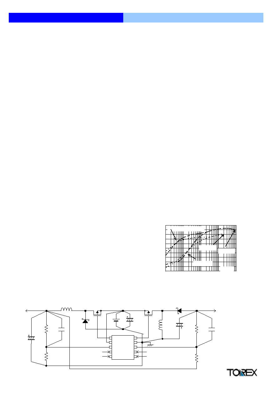
Typical Application
( XC9505B092A Input: 2 Cell, Output
1
: 3.3V, Output
2
: -7.5V )
XC9505 Series
2ch. Step-Down / Inverting DC/DC Controller ICs
Can be set freely with 0.9V(±
2.0%) of reference voltage
supply & external components
Can be set freely with 0.9V(±
2.0%) of reference voltage &
external components
more than 1000mA (VIN=5.0V,VOUT=3.3V)
more than - 100mA (VIN=5.0V,VOUT=- 7.5V)
The XC9505 series are PWM control, PWM/PFM switching, 2
channel (step-down and inverting) DC/DC controller ICs.
With 0.9V of standard voltage supply internal, and using
externally connected components, the output 1 voltage (step-
down DC/DC controller) can be set freely within a range of 0.9V
~ 6.0V. Since output 2 (inverting DC/DC controller) has a
built-in 0.9V reference voltage (accuracy
±
2), a negative voltage
can be set with the external components.
With a 180kHz frequency, the size of the external components
can be reduced. Switching frequencies of 300kHz and 500kHz
are also available as custom-designed products.
The control of the XC9505 series can be switched between
PWM control and PWM/PFM automatic switching control using
external signals. Control switches from PWM to PFM during
light loads when automatic switching is selected and the series
is highly efficient from light loads through to large output
currents. Noise is easily reduced with PWM control since the
frequency is fixed.
The series gives freedom of control selection so that control
suited to the application can be selected.
Soft-start time is internally set to 10msec (output 1)
which offers protection against rush currents and voltage
overshoot when the power is switched on .
0
10
20
30
40
50
60
70
80
90
100
0.1
1
10
100
1000
Output Current 1,2 I
OUT1,2
(mA)
Ef
f
i
c
i
enc
y
1,
2 EF
F
I
1,
2 (%)
PWM Control
PWM/PFM Switching Control
XC9505B092A (180kHz,V
OUT1
:3.3V,V
OUT2
:-7.5V)
V
IN
=5.0V
V
OUT1
:3.3V
V
OUT2
:-7.5V
Tr1,Tr2:XP162A12A6P, CL1, CL2=92uF(Tantalum),SD1:CMS02
SD2:MA2Q737,L1=47uH(CDRH6D28),L2=22uH(CDRH5D28)
L1:22uH
CDRH5D28
Tr2:Pch MOSFET
X P 1 6 2A 12 A 6P
CIN
:47uF
V IN
=5.0V
Tr1:Pch MOSFET
X P 16 2 A 1 2 A 6 P
SD2
:MA2Q737
SD1
:MA2Q737
RF B 1 1
:2 00k
CF B 1
:62pF
RF B 1 2
: 75k
V OUT1 : 3. 3V
1 EXT 1/
2 VDD
3 FB1
FB2 8
GND 9
EXT 2/ 10
4 PW M1
PW M2 7
5 EN1
EN2 6
CL 1 :47uF
CL 2:47uF
V P W M 1
V P W M 2
V EN 2
V EN 1
L2:22uH
CDRH5D28
V OUT2 :-7.5V
CF B 1
:88pF
RF B 2 1
:150 k
RF B 22
:43 k
1

Pin Configuration
Pin Assignment
Ordering Information
XC9505
123456
FB Voltage
0.9V
Embossed Tape
Embossed Tape
10
EXT2/
Channel 2 : External Transistor Drive Pin <Connected to Pch Power MOSFET Gate>
9
GND
Ground
PIN NUMBER
PIN NAME
FUNCTIONS
7
PWM2
Channel 2 : PWM/PFM Switching Pin <Control Output 2. PWM control when connected to
VDD, PWM / PFM auto switching when connected to Ground.>
8
FB2
Channel 2 : Output Voltage Monitor Feedback Pin <Threshold value : 0.9V. Output voltage
can be set freely by connecting split resistors between VOUT2 and VOUT1.>
5
EN1
Channel 1 : Enable Pin <Connected to Ground when Output 1 is in stand-by mode.
Connected to VDD when Output 1 is active. EXT1 is high when in stand-by mode.>
6
EN2
Channel 2 : Enable Pin <Connected to Ground when Output 2 is in stand-by mode.
Connected to VDD when Output 2 is active. EXT2/ is high when in stand-by mode.>
3
FB1
Channel 1 : Output Voltage Monitor Feedback Pin <Threshold value : 0.9V. Output voltage
can be set freely by connecting split resistors between VOUT1 and Ground.>
4
PWM1
Channel 1 : PWM/PFM Switching Pin <Control Output 1. PWM control when connected to
V
DD
, PWM / PFM auto switching when connected to Ground. >
1
EXT 1
Channel 1: External Transistor Drive Pin <Connected to Pch Power MOSFET Gate>
2
V
DD
Supply Voltage
4
5
3
180kHz
300kHz (custom)
500kHz (custom)
DESIGNATOR SYMBOL
DESCRIPTION
2
3
L
Reverse Feed
5
R
Package
MSOP-10
Standard Feed
6
A
9
Oscillation Frequency
2
0
1
B
Standard (10 Pin)
XC9505 Series
2ch. Step-Down / Inverting DC/DC Controller ICs
1 EXT1
2 VDD
3 FB1
FB2 8
GND 9
EXT2 10
4 PWM1
PWM2 7
5 CE1
CE2 6
MSOP-10
(TOP VIEW)
EN1
EN2
2
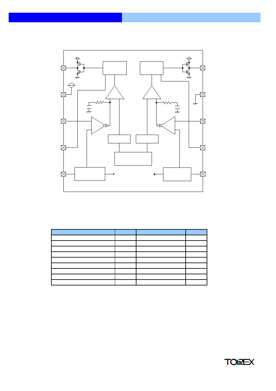
Block Diagram
Absolute Maximum Ratings
XC9505 Series
2ch. Step-Down / Inverting DC/DC Controller ICs
Ta=25
O
C
Tstg
- 55 ~ + 125
O
C
Pd
150
mW
mA
- 0.3 ~ V
DD
+ 0.3
- 0.3 ~ 12
V
Power Dissipation
IEXT
± 100
EXT1, 2 Pin Current
EXT1, 2 Pin Voltage
VEXT
Storage Temperature
Topr
- 40 ~ + 85
O
C
Operating Ambient Temperature
V
PWM1,2 Pin Voltage
VEN
- 0.3 ~ 12
V
EN1, 2 Pin Voltage
VPWM
VFB
- 0.3 ~ 12
V
FB1, 2 Pin Voltage
VDD
- 0.3 ~ 12
V
V
DD
Pin Voltage
SYMBOL
RATINGS
UNITS
PARAMETER
PWM1
+
-
+
-
FB1
VDD
EXT1
+
-
PWM/PFM
Controller1
Vref2=0.9V,
CE2
-
+
PWM/PFM
Controller2
FB2
GND
EXT2/
OSC
Generator
Ramp Wave
Generator1
Ramp Wave
Generator2
Error Amp2
Error Amp1
PWM
Comparator2
PWM
Comparator1
CE1
PWM2
CE2
Vref1=0.9V
with Soft Start1,
CE1
CE1 to
internal circuit
CE2 to
internal circuit
EN1
EN1
EN2
EN
EN1
EN
3
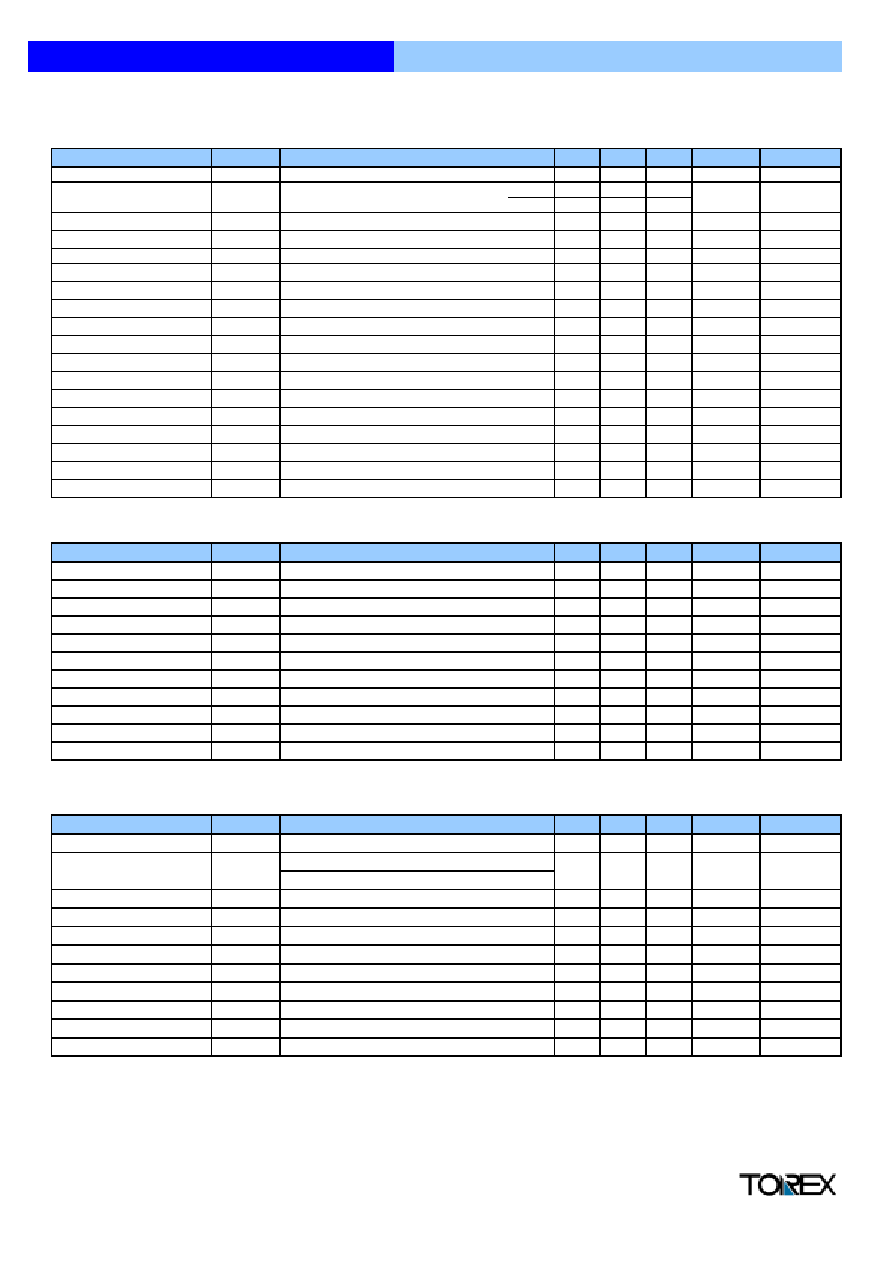
Electrical Characteristics
XC9505B092A
Common Characteristics
V
DD
2.0V, I
OUT1, 2
=1mA
Unless otherwise stated, V
DD
=3.0V, PWM1, 2=3.0V, EN1, 2 = 3.0V
Output 1 Characteristics
Step-Down Controller
Unless otherwise stated, V
DD
=EN1=PWM1=3.0V, EN2=PWM2=GND, EXT2=OPEN, FB2=OPEN, V
IN
=1.8V
Output 2 Characteristics
Inverting DC/DC Controller
I
OUT
2=1.0mA, RFB11=200k
, RFB12=75k
RFB21=17.5k
, RFB22=10k
, EN1=PWM1=3.0V
Unless otherwise stated, V
DD
=EN2=PWM2=3.0V, PWM1=EN1=GND, EXT1=OPEN, FB1=OPEN, V
IN
=3.0V
3)
4)
Please be careful not to exceed the breakdown voltage level of the peripheral parts.
EFFI1, 2={ [ (Output voltage) x (Output current) ] / [ (Input voltage) x (Input Current) ] } x 100
80
150
µ
A
2
70
120
µ
A
2
FB1=0V, FB2=0V
FB1=1.2V, FB2=1.2V
-
-
Supply Current 1-3
Supply Current 1-4
I
DD1-3
I
DD1-4
2
Minimum Duty Ratio2
MINDTY3 Same as I
DD
2
-
-
0
%
2
-
Minimum Duty Ratio1
MAXDTY2 Same as I
DD
2
-
-
-
%
V
1
VST1-2
-
2.0
V
OUT1
V
OUT2
-
VIN
80
160
EN2=3.0V, EN1=0, FB2=1.2V
TEST CIRCUIT
PARAMETER
SYMBOL
CONDITIONS
MIN.
V
TYP.
MAX.
UNITS
2.0
-
10.0
Output Voltage Range
(note 1)
V
OUTSET
0.9
-
Supply Current 1
I
DD1
FB=0V, FB2=1.2V
-
µ
A
2
EN1=3.0V, EN2=0, FB1=0V
-
µ
A
2
Supply Current 1-1
I
DD1-1
50
110
-
Supply Current 1-2
I
DD1-2
60
120
µ
A
2
Supply Current 2
I
DD2
FB1=1.2V, FB2=0V
-
70
130
µ
A
2
Stand-by Current
I
STB
Same as I
DD1
, EN1=EN2=0V
-
1.0
3.0
µ
A
2
Oscillation Frequency
FOSC
Same as I
DD1
153
180
207
kHz
2
EN1, 2 "High" Voltage
V
ENH
FB1=0V, FB2=3.0V
0.65
-
-
V
2
EN1, 2 "Low" Voltage
V
ENL
FB1=0V, FB2=3.0V
-
-
0.20
V
2
EN1, 2 "High" Current
I
ENH
FB1=3.0V, FB2=0V
-
-
0.50
µ
A
2
EN1, 2 "Low" Current
I
ENL
EN1, 2=0V, FB1=3.0V, FB2=0V
-
-
-0.50
µ
A
2
PWM1, 2 "High" Current
I
PWMH
FB1=3.0V, FB2=0V, PWM1, 2=3.0V
-
-
0.50
µ
A
2
PWM1, 2 "Low" Current
I
PWML
FB1=3.0V, FB2=0V, PWM1, 2=0V
-
-
-0.50
µ
A
2
FB1, 2 "High" Current
I
FBH
FB1=3.0V, FB2=0.8V
-
-
0.50
µ
A
2
FB1, 2 "Low" Current
V
FBL
FB1=1.0V, FB2=0V
-
-
-0.50
µ
A
2
PARAMETER
SYMBOL
CONDITIONS
MIN.
TYP.
MAX.
UNITS
TEST CIRCUIT
FB1 Voltage
VFB1
V
DD
=3.0V, V
IN
=1.5V, I
OUT1
=10mA
0.882 0.900 0.918
V
3
Minimum Operating Voltage
VINmin1
-
-
2
V
1
Maximum Duty Ratio1
MINDTY1 Same as I
DD
1
100
-
-
%
2
PFM Duty Ratio1
PFMDTY1 No Load, VPWM1=0V
22
30
38
%
4
Efficiency1 (note 2)
EFFI1
I
OUT1
= 250mA, Pch MOSFET: XP162A12A6P
-
92
-
%
4
Soft-Start Time1
T
SS1
VOUT1
◊
0.95V, EN1=0V
0.65V
5.0
10.0
20.0
msec
4
EXT1 "High" ON Resistance R
EXTBH1
FB1=0V, EXT1=V
DD
-0.4V
-
28
47
5
EXT1 "Low" ON Resistance
R
EXTBL1
EN1=FB1=1.2V, EXT1=0.4V
-
22
30
5
PWM1 "High" Voltage
V
PWMH1
No Load
0.65
-
-
V
4
PWM1 "Low" Voltage
V
PWML1
No Load
-
-
0.20
V
4
PARAMETER
SYMBOL
CONDITIONS
MIN.
TYP.
MAX.
UNITS
TEST CIRCUIT
-
-
FB2 Voltage
VFB2
V
DD
=3.0V
0.882
Operation Start-up
Voltage2
2
Maximum Duty Ratio2
MAXDTY2 Same as I
DD
1
75
80
87
%
2
FB2=1.2V
30
38
%
Oscillation Start-up Voltage2
PFM Duty Ratio2
PFMDTY2 No Load, V
PWM2
=0V
2.0
V
VST2-2
6
Efficiency2 (Note 2)
EFFI2
I
OUT2
= -150mA, Pch MOSFET: XP162A12A6P
-
76
-
%
6
22
EXT2 "High" ON Resistance R
EXTBH2
EN2=FB2= 0V, EXT2=V
DD
-0.4V
-
28
47
5
30
5
EXT2 "Low" ON Resistance
R
EXTBL2
FB2=3.0V, EXT2=0.4V
-
22
6
PWM2 "High" Voltage
V
PWMH2
No Load
0.65
-
-
V
6
PWM2 "Low" Voltage
V
PWML2
No Load
-
-
0.20
V
XC9505 Series
2ch. Step-Down / Inverting DC/DC Controller ICs
Ta=25
O
C
1
-
0.0
V
Supply Voltage
V
DD
Ta=25
O
C
Ta=25
O
C
0.900 0.918
V
2
4

Electrical Characteristics
XC9505B093A
Common Characteristics
V
DD
2.0V, I
OUT1, 2
=1mA
Unless otherwise stated, V
DD
=3.0V, PWM1, 2=3.0V, EN1, 2 = 3.0V
Output 1 Characteristics
Step-Down Controller
Unless otherwise stated, V
DD
=EN1=PWM1=3.0V, EN2=PWM2=GND, EXT2=OPEN, FB2=OPEN, V
IN
=1.8V
Output 2 Characteristics
Inverting DC/DC Controller
I
OUT
2=1.0mA, RFB11=200k
, RFB12=75k
RFB21=17.5k
, RFB22=10k
, EN1=PWM1=3.0V
Unless otherwise stated, V
DD
=EN2=PWM2=3.0V, PWM1=EN1=GND, EXT1=OPEN, FB1=OPEN, V
IN
=3.0V
3)
4)
6
Efficiency2 (Note 2)
EFFI2
I
OUT2
= -150mA, Pch MOSFET: XP162A12A6P
-
2
PFM Duty Ratio2
PFMDTY2 No Load, V
PWM2
=0V
22
30
38
%
6
-
-
2.0
V
Ta=25
O
C
Operation Start-up
Voltage2
VST1-2
-
-
2.0
V
1
2
Minimum Duty Ratio1
MAXDTY2 Same as I
DD
2
-
MAX.
UNITS
TEST CIRCUIT
VFB1
V
DD
=3.0V, V
IN
=1.5V, I
OUT1
=10mA
0.882 0.900 0.918
V
3
180
µ
A
-
1.0
3.0
µ
A
Supply Current 1-1
I
DD1-1
EN1=3.0V, EN2=0, FB1=0V
µ
A
60
120
-
Supply Current 1
I
DD1
FB=0V, FB2=1.2V
µ
A
100
190
-
Output Voltage Range
(note 1)
V
OUTSET
V
OUT1
0.9
V
OUT2
-
XC9505 Series
2ch. Step-Down / Inverting DC/DC Controller ICs
EFFI1, 2={ [ (Output voltage) x (Output current) ] / [ (Input voltage) x (Input Current) ] } x 100
Please be careful not to exceed the breakdown voltage level of the peripheral parts.
-
0.20
V
6
PWM2 "Low" Voltage
V
PWML2
No Load
-
-
-
V
6
PWM2 "High" Voltage
V
PWMH2
No Load
0.65
5
EXT2 "Low" ON Resistance
R
EXTBL2
FB2=3.0V, EXT2=0.4V
-
22
30
5
EXT2 "High" ON Resistance R
EXTBH2
EN2=FB2= 0V, EXT2=V
DD
-0.4V
-
28
47
-
0
%
75
-
%
2
Minimum Duty Ratio2
MINDTY3 Same as I
DD
2
-
Maximum Duty Ratio2
MAXDTY2 Same as I
DD
1
75
80
87
%
2
Oscillation Start-up Voltage2
0.900 0.918
V
FB2 Voltage
VFB2
V
DD
=3.0V
0.882
VST2-2
FB2=1.2V
TYP.
MAX.
UNITS
TEST CIRCUIT
PARAMETER
SYMBOL
CONDITIONS
MIN.
-
0.20
V
4
PWM1 "Low" Voltage
V
PWML1
No Load
-
-
-
V
4
PWM1 "High" Voltage
V
PWMH1
No Load
0.65
22
30
5
EXT1 "Low" ON Resistance
R
EXTBL1
EN1=FB1=1.2V, EXT1=0.4V
-
4
EXT1 "High" ON Resistance R
EXTBH1
FB1=0V, EXT1=V
DD
-0.4V
-
28
47
5
-
%
4
Soft-Start Time1
T
SS1
VOUT1
◊
0.95V, EN1=0V
0.65V
5.0
10.0
20.0
msec
2
22
30
38
%
4
-
-
%
I
OUT1
= 250mA, Pch MOSFET: XP162A12A6P
-
92
PFM Duty Ratio1
PFMDTY1
Efficiency1 (note 2)
No Load, VPWM1=0V
EFFI1
-
100
%
2
Maximum Duty Ratio1
MINDTY1 Same as I
DD
1
-
Minimum Operating Voltage
VINmin1
-
-
2.0
V
1
FB1 Voltage
-
-0.50
µ
A
Ta=25
O
C
PARAMETER
SYMBOL
CONDITIONS
MIN.
TYP.
2
FB1, 2 "Low" Current
V
FBL
FB1=1.0V, FB2=0V
-
-
0.50
µ
A
2
FB1, 2 "High" Current
I
FBH
FB1=3.0V, FB2=0.8V
-
-
-0.50
µ
A
2
PWM1, 2 "Low" Current
I
PWML
FB1=3.0V, FB2=0V, PWM1, 2=0V
-
-
0.50
µ
A
2
PWM1, 2 "High" Current
I
PWMH
FB1=3.0V, FB2=0V, PWM1, 2=3.0V
-
-
-0.50
µ
A
2
EN1, 2 "Low" Current
I
ENL
EN1, 2=0V, FB1=3.0V, FB2=0V
-
-
0.50
µ
A
2
EN1, 2 "High" Current
I
ENH
FB1=3.0V, FB2=0V
-
-
0.20
V
2
EN1, 2 "Low" Voltage
V
ENL
FB1=0V, FB2=3.0V
-
-
-
V
2
EN1, 2 "High" Voltage
V
ENH
FB1=0V, FB2=3.0V
0.65
300
345
kHz
2
Oscillation Frequency
FOSC
Same as I
DD1
255
Supply Current 2
I
DD2
-
Stand-by Current
I
STB
Same as I
DD1
, EN1=EN2=0V
µ
A
2
2
FB1=1.2V, FB2=0V
80
150
µ
A
2
-
100
2
FB1=0V, FB2=0V
Supply Current 1-3
I
DD1-3
-
Supply Current 1-4
I
DD1-4
FB1=1.2V, FB2=1.2V
80
140
80
150
µ
A
2
Supply Current 1-2
I
DD1-2
EN2=3.0V, EN1=0, FB2=1.2V
-
2
2
-
VIN
V
1
-
0.0
-
10.0
V
Supply Voltage
V
DD
2.0
Ta=25
O
C
PARAMETER
SYMBOL
CONDITIONS
MIN.
TYP.
MAX.
UNITS
TEST CIRCUIT
5

Electrical Characteristics
XC9505B095A
Common Characteristics
V
DD
2.0V, I
OUT1, 2
=1mA
Unless otherwise stated, V
DD
=3.0V, PWM1, 2=3.0V, EN1, 2 = 3.0V
Output 1 Characteristics
Step-Down Controller
Unless otherwise stated, V
DD
=EN1=PWM1=3.0V, EN2=PWM2=GND, EXT2=OPEN, FB2=OPEN, V
IN
=1.8V
Output 2 Characteristics
Inverting DC/DC Controller
I
OUT
2=1.0mA, RFB11=200k
, RFB12=75k
RFB21=17.5k
, RFB22=10k
, EN1=PWM1=3.0V
Unless otherwise stated, V
DD
=EN2=PWM2=3.0V, PWM1=EN1=GND, EXT1=OPEN, FB1=OPEN, V
IN
=3.0V
3)
4)
6
Efficiency2 (Note 2)
EFFI2
I
OUT2
= -150mA, Pch MOSFET: XP162A12A6P
-
2
PFM Duty Ratio2
PFMDTY2 No Load, V
PWM2
=0V
22
30
38
%
6
-
-
2.0
V
Ta=25
O
C
Operation Start-up
Voltage2
VST1-2
-
-
2.0
V
1
2
3
Minimum Duty Ratio1
MAXDTY2 Same as I
DD
2
-
-
-
%
µ
A
Ta=25
O
C
PARAMETER
SYMBOL
CONDITIONS
MIN.
TYP.
MAX.
UNITS
TEST CIRCUIT
2
130
250
-
140
230
µ
A
Supply Current 1-1
I
DD1-1
EN1=3.0V, EN2=0, FB1=0V
µ
A
Output Voltage Range
(note 1)
V
OUTSET
Supply Current 1
I
DD1
FB=0V, FB2=1.2V
µ
A
2
EFFI1, 2={ [ (Output voltage) x (Output current) ] / [ (Input voltage) x (Input Current) ] } x 100
Please be careful not to exceed the breakdown voltage level of the peripheral parts.
-
0.20
V
6
PWM2 "Low" Voltage
V
PWML2
No Load
-
-
-
V
6
PWM2 "High" Voltage
V
PWMH2
No Load
0.65
5
EXT2 "Low" ON Resistance
R
EXTBL2
FB2=3.0V, EXT2=0.4V
-
22
30
5
EXT2 "High" ON Resistance R
EXTBH2
EN2=FB2= 0V, EXT2=V
DD
-0.4V
-
28
47
-
0
%
71
-
%
2
Minimum Duty Ratio2
MINDTY3 Same as I
DD
2
-
Maximum Duty Ratio2
MAXDTY2 Same as I
DD
1
75
80
87
%
2
Oscillation Start-up Voltage2
0.900 0.918
V
FB2 Voltage
VFB2
V
DD
=3.0V
0.882
VST2-2
FB2=1.2V
TYP.
MAX.
UNITS
TEST CIRCUIT
PARAMETER
SYMBOL
CONDITIONS
MIN.
-
0.20
V
4
PWM1 "Low" Voltage
V
PWML1
No Load
-
-
-
V
4
PWM1 "High" Voltage
V
PWMH1
No Load
0.65
22
30
5
EXT1 "Low" ON Resistance
R
EXTBL1
EN1=FB1=1.2V, EXT1=0.4V
-
4
EXT1 "High" ON Resistance R
EXTBH1
FB1=0V, EXT1=V
DD
-0.4V
-
28
47
5
-
%
4
Soft-Start Time1
T
SS1
VOUT1
◊
0.95V, EN1=0V
0.65V
5.0
10.0
20.0
msec
2
22
30
38
%
4
I
OUT1
= 250mA, Pch MOSFET: XP162A12A6P
-
91
PFM Duty Ratio1
PFMDTY1
Efficiency1 (note 2)
No Load, VPWM1=0V
EFFI1
-
100
%
2
Maximum Duty Ratio1
MINDTY1 Same as I
DD
1
Minimum Operating Voltage
VINmin1
-
-
2.0
V
1
FB1 Voltage
-
-0.50
µ
A
VFB1
V
DD
=3.0V, V
IN
=1.5V, I
OUT1
=10mA
0.882 0.900 0.918
V
2
FB1, 2 "Low" Current
V
FBL
FB1=1.0V, FB2=0V
-
-
0.50
µ
A
2
FB1, 2 "High" Current
I
FBH
FB1=3.0V, FB2=0.8V
-
-
-0.50
µ
A
2
PWM1, 2 "Low" Current
I
PWML
FB1=3.0V, FB2=0V, PWM1, 2=0V
-
-
0.50
µ
A
2
PWM1, 2 "High" Current
I
PWMH
FB1=3.0V, FB2=0V, PWM1, 2=3.0V
-
-
-0.50
µ
A
2
EN1, 2 "Low" Current
I
ENL
EN1, 2=0V, FB1=3.0V, FB2=0V
-
-
0.50
µ
A
2
EN1, 2 "High" Current
I
ENH
FB1=3.0V, FB2=0V
-
-
0.20
V
2
EN1, 2 "Low" Voltage
V
ENL
FB1=0V, FB2=3.0V
-
-
-
V
2
EN1, 2 "High" Voltage
V
ENH
FB1=0V, FB2=3.0V
0.65
500
575
kHz
2
Oscillation Frequency
FOSC
Same as I
DD1
425
Supply Current 2
I
DD2
-
Stand-by Current
I
STB
Same as I
DD1
, EN1=EN2=0V
-
µ
A
2
2
FB1=1.2V, FB2=0V
100
190
µ
A
2
1.0
3.0
2
FB1=0V, FB2=0V
Supply Current 1-3
I
DD1-3
-
Supply Current 1-4
I
DD1-4
FB1=1.2V, FB2=1.2V
100
170
110
220
µ
A
2
Supply Current 1-2
I
DD1-2
EN2=3.0V, EN1=0, FB2=1.2V
-
80
150
-
-
V
1
-
0.0
V
OUT1
0.9
V
OUT2
-
-
-
TEST CIRCUIT
Supply Voltage
V
DD
2.0
-
10.0
V
XC9505 Series
2ch. Step-Down / Inverting DC/DC Controller ICs
Ta=25
O
C
PARAMETER
SYMBOL
CONDITIONS
MIN.
TYP.
MAX.
UNITS
6

Operational Description
<Error Amp. 1>
<Error Amp. 2>
<OSC Generator>
<Ramp Wave Generator 1, 2>
The Ramp Wave Generator generates a saw-tooth waveform based on outputs from the OSC Generator.
<PWM Comparator 1, 2>
<PWM/PFM Controller 1, 2>
<Vref 1 with Soft Start 1>
<Vref 2>
The reference voltage, Vref2 (FB2 pin voltage)=0.9V, is adjusted and fixed by laser trimming.
<Enable Function 1,2>
This circuit generates PFM pulses.
Control can be switched between PWM control and PWM/PFM automatic switching control using external signals.
The PFM/PWM automatic switching mode is selected when the voltage of the PWM1 (2) pin is less than 0.2V, and the control switches
between PWM and PFM automatically depending on the load. As the PFM circuit generates pulses based on outputs from the PWM
Comparator, shifting between modes occurs smoothly. PWM control mode is selected when the voltage of the PWM1 (2) pin is more than
0.65V. Noise is easily reduced with PWM control since the switching frequency is fixed.
Control suited to the application can easily be selected which is useful in audio applications, for example, where traditionally, efficiencies
have been sacrificed during stand-by as a result of using PWM control (due to the noise problems associated with the PFM mode in stand-
by).
This function controls the operation and shutdown of the IC. When the voltage of the EN1 or EN2 pins is 0.2V or less, the mode will
be disable, the channel's operations will stop and the EXT1 and the EXT2 pin will be kept at a high level (the external P-type
MOSFET will be OFF). When both EN1 and EN2 are in a state of chip disable, current consumption will be no more than 3.0
µ
A.
When the EN1 or EN2 pin's voltage is 0.65V or more, the mode will be enable and operations will recommence. With channel one
(output 1) soft-start, 95% of the set output voltage will be reached within 10msec (TYP) from the moment of enable.
XC9505 Series
2ch. Step-Down / Inverting DC/DC Controller ICs
This circuit generates the internal reference clock.
Error Amplifier 2 is designed to monitor the output voltage and it compares the feedback voltage 2 (FB2) with the reference voltage Vref 2.
In response to feedback of a voltage lower than the reference voltage Vref2, the output voltage of the error amp. decreases.
The XC9505 series are dual DC/DC (step-down + inverting) converter controller ICs with built-in high speed, low ON resistance buffers.
Error Amplifier 1 is designed to monitor the output voltage and it compares the feedback voltage 1 (FB1) with the reference voltage Vref1.
In response to feedback of a voltage lower than the reference voltage Vref1, the output voltage of the error amp. decreases.
The PWM Comparator compares outputs from the Error Amp. and saw-tooth waveform. When the voltage from the Error Amp's output is
low, the external switch will be set to ON.
The reference voltage, Vref1(FB1 pin voltage)=0.9V, is adjusted and fixed by laser trimming (for output voltage settings, please refer to the
functional settings notes on page 9.). To protect against inrush current, when the power is switched on, and also to protect against voltage
overshoot, soft-start time is set internally to 10ms. It should be noted, however, that this circuit does not protect the load capacitor (CL)
from inrush current. With the Vref voltage limited, and depending upon the input to error amp 1, the operation maintains a balance between
the two inputs of error amps and controls the EXT pin's ON time so that it doesn't increase more than is necessary.
7

Functional Settings
< Output Voltage Setting, Ch.1 (Step-up DC/DC Converter Controller) >
V
OUT
1=0.9
◊
(RFB11+RFB12) / RFB12
[Calculation Example]
When RFB11=220k
and RFB12=75k
:
V
OUT
1=0.9
◊
(200k+75k) / 75k=3.3V.
[Typical Example]
< Output Voltage Setting, Ch.2 (Inverting DC/DC Converter) >
V
OUT
2 = (0.9 - V
OUT
1) x (RFB21 / RFB22) + 0.9V
[Calculation Example]
When RFB21=17.5k
,
RFB22=10k
,
V
OUT
1=3.3V, V
OUT
2= - 3.3V
The value of speed-up capacitor for phase compensation CFB21 :
[Conditions: Heavy load (when coil current is continous.)]
fzfb2 = 1/2 x
x CFB21 x RFB21) = 10kHz
[Conditions: Light load (when coil current is discontinous.)]
Less than CFB21=0.1
µ
F
Depending on the application, the inductance value L, and the load capacity value CL, adjustments to this value are suggested.
> Example Circuit 1 : Using voltage of Ch 1 (Step-Down)
> Example Circuit 1 : Using a positive regulator
VOUT2 = (0.9 - VROUT) x (RFB21 / RFB22) + 0.9V
Channel 1 (Step-Down) circuits should be enable by setting EN1 to
High level so that a stable voltage is provided. Inrush current to the
inverter when the supply voltage VDD of the IC is 2.0 V or higher can
be controlled by setting EN 1 and EN 2 to enable ("H" level)
simultaneously.
A stable positive voltage produced by a positive-voltage regulator or
by other means is usable.
Depending on the application, the inductance value L, and the load capacity value CL, adjustments to this value are suggested so that the
value is somewhere between 1kHz to 50kHz.
2.0
2.2
VOUT
(V)
5.0
3.0
3.3
VOUT
(V)
1.0
1.5
1.8
220
220
62
560
240
24
180
33
33
220
330
62
360
2.7
30
270
430
390
220
2.5
RFB12
(k
)
CFB1
(pF)
2ch. Step-Down / Inverting DC/DC Controller ICs
RFB11
(k
)
RFB12
(k
)
CFB1
(pF)
RFB11
(k
)
Output voltage can be set by adding reference voltage and split resistors externally. Output voltage is determined using the following
equation and is based on the values of RFB21 and RFB22. The sum of RFB21 and RFB22 should normally be 500k
or less. The
equation uses Ch 1's (V
OUT1
) output voltage calculation method for the reference voltage.
XC9505 Series
390
270
33
82
18
160
200
75
62
The speed-up capacitor for phase compensation's (CFB1) value should be adjusted using the formula fzfb=1/(2
◊◊
CFB1
◊
RFB11) so that it
equals 12kHz. Depending on the application, the inductance value L, and the load capacity value CL, adjustments to this value are
suggested so that the value is somewhere between 1kHz to 50kHz.
Output voltage can be set by adding external split resistors. Output voltage is determined by the following equation, based on the values of
RFB11 and RFB12. The sum of RFB11 and RFB12 should normally be 1 M
or less.
330
270
39
SBD2
RFB21
CFB21
VOUT2
CL2
RFB22
VOUT1
FB2
Inside of XC9505 IC
SBD2
RFB21
CFB21
VOUT2
CL2
RFB22
FB2
Inside of
XC9505 IC
VR
To the other
circuit
VR_OUT
8

External Components
Conditions : Light load (when coil current is discontinuous.)
Channel One (Step-Down DC/DC Converter Controller)
Channel Two (Inverter DC/DC Controller)
Tr 1 :
* MOSFET
Tr 2 :
* MOSFET
XP152A12C0
(TOREX P-Channel Power MOSFET)
XP152A12C0
(TOREX P-Channel Power MOSFET)
SD 1 :
CRS02
(Schottky , TOSHIBA)
SD 2 :
CRS02
(Schottky, TOSHIBA)
L1 :
10
µ
H
(SUMIDA, CDRH4D18C,
L2 :
10
µ
H
(SUMIDA, CDRH4D18C,
TOKO, D412F, FOSC = 500kHz)
TOKO, D412F, FOSC = 500kHz)
15
µ
H
(SUMIDA, CDRH4D18C,
15
µ
H
(SUMIDA, CDRH4D18C,
TOKO, D412F, FOSC = 300kHz)
TOKO, D412F, FOSC = 300kHz)
22
µ
H
(SUMIDA, CDRH4D18C,
22
µ
H
(SUMIDA, CDRH4D18C,
TOKO, D412F, FOSC = 180kHz)
TOKO, D412F, FOSC = 180kHz)
Please set so that the coil current is discontinous.
Please set so that the coil current is discontinous.
CL1 :
10V, 4.7
µ
F
(Ceramic)
CL2 :
10V, 4.7
µ
F
(Ceramic)
*PNP Tr
*PNP Tr
2SA1213
(TOSHIBA)
2SA1213
(TOSHIBA)
RB1 :
500
RB 2 :
500
CB1 :
2200pF
(Ceramic)
CB 2 :
2200pF
(Ceramic)
CB1
(2
x RB2 x FOSC x 0.7)
CB2
(2
x RB2 x FOSC x 0.7)
Conditions: Heavy load (when coil current is continous.)
Channel One (Step-Down DC/DC Converter Controller)
Channel Two (Inverter DC/DC Controller)
Tr 1 :
* MOSFET
Tr 2 :
* MOSFET
XP162A12A6P (TOREX P-Channel Power MOSFET)
XP162A12A6P (TOREX P-Channel Power MOSFET)
SD 1 :
MA2Q737
(Schottky , MATSUSHITA)
SD 2 :
MA2Q737
(Schottky, MATSUSHITA)
CMS02
(Schottky , TOSHIBA)
CRS02, CMS02
(Schottky , TOSHIBA)
L1 :
10
µ
H
(SUMIDA, CDRH5D28, FOSC = 500kHz)
L2 :
10
µ
H
(SUMIDA, CDRH5D28, FOSC = 500kHz)
22
µ
H
(SUMIDA, CDRH5D28, FOSC = 300kHz)
15
µ
H
(SUMIDA, CDRH5D28, FOSC = 300kHz)
47
µ
H
(SUMIDA, CDRH5D28, FOSC = 180kHz)
22
µ
H
(SUMIDA, CDRH5D28, FOSC = 180kHz)
CL1 :
16V, 47
µ
F
(Tantalum)
CL2 :
16V, 47
µ
F
(Tantalum)
CL = (CL standard value ) x (IOUT1 (mA) / 500mA x VOUT1 / VIN)
CL = (CL standard value ) x (IOUT2 (mA) / 150mA x VOUT2 / VIN)
*PNP Tr
*PNP Tr
2SA1213
(TOSHIBASANYO)
2SA1213
(TOSHIBA)
RB1 :
500
RB 2 :
500
CB1 :
2200pF
(Ceramic)
CB 2 :
2200pF
(Ceramic)
CB1
(2
x RB2 x FOSC x 0.7)
CB2
(2
x RB2 x FOSC x 0.7)
Increase capacity according to the equation below
when the step-up voltage ratio is large and output
current is high.
Increase capacity according to the equation below
when the step-up voltage ratio is large and output
current is high.
Adjust in accordance with load &
Tr.'s HFE
Adjust in accordance with load &
Tr.'s HFE
RB1
(VIN-0.7) x (hFE/IC-REXTBL)
RB2
(VIN-0.7) x (hFE/IC-REXTBL)
RB1
(VIN-0.7) x (hFE/IC-REXTBL)
RB2
(VIN-0.7) x (hFE/IC-REXTBL)
Note : VGS Breakdown Voltage of this Tr. is 12V so
please be careful with the power supply voltage.
2ch. Step-Down / Inverting DC/DC Controller ICs
Adjust in accordance with load &
Tr.'s HFE
Adjust in accordance with load &
Tr.'s HFE
XC9505 Series
Note : VGS Breakdown Voltage of this Tr. is 12V so
please be careful with the power supply voltage.
Note : VGS Breakdown Voltage of this Tr. is 12V so
please be careful with the power supply voltage.
Note : VGS Breakdown Voltage of this Tr. is 12V so
please be careful with the power supply voltage.
9

Notes on how to use
Hint on application
1. Channel 2 ( Inverting )
Soft start circuit
> Example of typical application circuit : Improved Soft start
Time to make soft start time is calculated by the equation below.
Example )
When VOUT1 = 3.3V and VOUT2 = - 7.5V,
RFB21 = 350k
, RFB22 = 100k
by the equation below.
VOUT2 = (0.9 - VOUT1) x (RFB21 / RFB22) + 0.9
When the light load, CFB21=0.1
µ
F or lower value can be used.
Therefore, when CFB21=0.027
µ
F,
Time_ss2 = 5.0mS and VOUT2 = 95% of setting value
2. Channel 2 (Inverting)
Withstand voltage of transistor
The voltage applied between the drain and source is the sum of VIN and VOUT 2.
Select a transistor with an absolute VDSS rating that is suitable for your operating conditions.
Example: The voltage applied across VDS of a transistor will be 20.0V if VIN = 5.0 V and VOUT 2 = -15.0 V.
This example is effective when EN 1 and EN 2 are enabled with different timings under light load condition (the coil current being
discontinuous).
Under this condition, a transistor with VDSS higher than 20.0V should be selected. (Use a transistor with VDSS
that is 1.5 times the applied voltage or more, as a standard.)
Channel 2 (inverting) is subject to the overshoot of output voltage 2 (VOUT 2) at start-up. It is possible to control the overshoot of
output voltage 2 (VOUT 2), as shown by circuit example 1 in "Output Voltage Settings for Channel 2" in "Function Settings."
In this
circuit configuration, EN 1 and EN 2 are enabled (set to "H" level) simultaneously. This lets output voltage 1 (VOUT 1) of channel 1
increase gently as soft start, thereby controlling the overshoot.
XC9505 Series
2ch. Step-Down / Inverting DC/DC Controller ICs
SBD2
VOUT1
FB2
Inside of
XC9505 IC
RFB21
CFB21
VOUT2
CL2
RFB22
EN2
ON/OFF
signal
Pch
MOSFET1
R1
Nch
MOSFET2
Time
SS2 =
- R
FB21
x C
CFB21
/ Ln 1 -
(0.9 - V
OUT2
) x R
FB22
)
(V
OUT1
- 0.9) x R
FB21
10

Test Circuits
XC9505 Series
2ch. Step-Down / Inverting DC/DC Controller ICs
Circuit 2
Circuit 3
Circuit 4
Circuit 5
Circuit 6
Pch
MOSFET
L2
20kW
20kW
R
L
V
IN
C
L2
+
V
OUT2
A
A
C
IN
1 EXT1
2 VDD
3 FB1
FB2 8
GND 9
EXT2/ 10
4 PWM1
PWM2 7
5 EN1
EN2 6
OSC
V
PWM1
V
EN1
A
1mF
V
DD
OSC
A
A
V
PWM2
A
A
V
EN2
1 EXT1
2 VDD
3 FB1
FB2 8
GND 9
EXT2/ 10
4 PWM1
PWM2 7
5 EN1
EN2 6
V
FB1
A
V
FB2
A
5
10W
2200pF
R
FB11
R
FB12
C
FB1
47mF
+
V
OUT1
510W
2200pF
L2
PNP
Tr
R
FB21
R
FB22
R
L2
C
L2
+
V
OUT2
R
L1
C
IN
1mF
C
FB2
+
4.8V
V
+
C
FB2
V
PWM1
V
EN1
V
EN1
V
PWM2
2 VDD
3 FB1
FB2 8
GND 9
EXT2/ 10
4 PWM1
PWM2 7
5 EN1
EN2 6
OSC
V
PWM1
V
EN1
1mF
V
DD
OSC
V
PWM2
V
EN2
1 EXT1
2 VDD
3 FB1
FB2 8
GND 9
EXT2 10
4 PWM1
PWM2 7
5 EN1
EN2 6
V
FB1
V
FB2
V
EXT1
V
EXT2
OSC
V
PWM2
V
EN2
SD2
Rp
Rp
SD2
1 EXT1/
Circuit 1
Circuit
Pch
MOSFET
L2
20kW
20kW
R
L
V
IN
C
L2
+
V
OUT2
A
A
C
IN
1 EXT1
2 VDD
3 FB1
FB2 8
GND 9
EXT2/ 10
4 PWM1
PWM2 7
5 EN1
EN2 6
OSC
V
PWM1
V
EN1
A
1mF
V
DD
OSC
A
A
V
PWM2
A
A
V
EN2
2 VDD
3 FB1
FB2 8
GND 9
EXT2/ 10
4 PWM1
PWM2 7
5 EN1
EN2 6
V
FB1
A
V
FB2
A
2200
pF
L1
R
FB11
R
FB12
C
FB1
47mF
+
V
OUT1
510W
2200pF
L2
PNP
Tr
R
FB21
R
FB22
R
L2
C
L2
+
V
OUT2
R
L1
C
IN
V
IN
1mF
C
FB2
+
4.8V
V
+
C
FB2
V
PWM1
V
EN1
V
EN1
V
PWM2
2 VDD
3 FB1
FB2 8
GND 9
EXT2/ 10
4 PWM1
PWM2 7
5 EN1
EN2 6
OSC
V
PWM1
V
EN1
1mF
V
DD
OSC
V
PWM2
V
EN2
1 EXT1
2 VDD
3 FB1
FB2 8
GND 9
EXT2 10
4 PWM1
PWM2 7
5 EN1
EN2 6
V
FB1
V
FB2
V
EXT1
V
EXT2
OSC
V
PWM2
V
EN2
SD1
SD2
Rp
Rp
SD2
1 EXT1/
1 EXT1/
R
L
V
IN
C
L1
V
OUT1
C
IN
A
2 VDD
3 FB1
FB2 8
GND 9
4 PWM1
PWM2 7
5 EN1
EN2 6
V
A
Pch
MOSFET1
R
L
V
IN
C
L1
V
OUT1
C
IN
A
2 VDD
3 FB1
FB2 8
GND 9
4 PWM1
PWM2 7
5 EN1
EN2 6
V
A
Pch
MOSFET1
62pF
SBD1
SBD1
200k
W
75kW
L1
L1
1 EXT1
EXT2 10
1 EXT1
EXT2 10
11

External Components of the Test Circuits
Circuits 1
L1, L2: 22
µ
H (SUMIDA CDRH5D28) : XC9505B092A
15
µ
H (SUMIDA CDRH5D28) : XC9505B093A
10
µ
H (SUMIDA CDRH5D28) : XC9505B095A
SD1, SD2 : CRS02 (Schottky, TOSHIBA)
EC10QS06 (Schottky, NIHON INTER)
CL1, CL2 : 16MCE476MD2 (Tantalum, NIHON CHEMICON)
35MCE335MB x 3 (Tantalum, NIHON CHEMICON)
CIN : 16MCE476MD2
PNP Tr 1 : 2SA1213 (TOSHIBA)
PNP Tr 2 : 2SA1213 (TOSHIBA)
RFB : Please use by the conditions as below.
RFB11 + RFB12
1M
RFB21 + RFB22
1M
RFB11 / RFB12 = (Setting Output Voltage / 0.9) - 1
VOUT2 = (0.9 - VOUT1) / (RFB21 / RFB22) + 0.9V
CFB : fzfb = 1 /(2 x
x CFB1 x RFB11) = 1kHz to 50kHz (12kHz usual)
fzfb = 1 /(2 x
x CFB2 x RFB21) = 1kHz to 50kHz (12kHz usual).
Circuits 3
L1 : 22
µ
H (SUMIDA CDRH5D28)
SD 1 : MA2Q737 (Schottky, MATSUSHITA)
CL 1 : 16MCE476MD2 (Tantalum, NIHONCHEMICON)
CIN : 16MCE476MD2 (Tantalum, NIHONCHEMICON)
Pch MOSFET : XP162A12A6P (TOREX)
Circuits 4
L1 : 22
µ
H (SUMIDA CDRH5D28) : XC9505B092A
15
µ
H (SUMIDA CDRH5D28) : XC9505B093A
10
µ
H (SUMIDA CDRH5D28) : XC9505B095A
SD 1 : MA2Q737 (Schottky, MATSUSHITA)
CL 1 : 16MCE476MD2 (Tantalum, NIHONCHEMICON)
CIN : 16MCE476MD2 (Tantalum, NIHONCHEMICON)
Pch MOSFET : XP162A12A6P (TOREX)
Circuits 6
L2 : 22
µ
H (SUMIDA CDRH5D28) : XC9505B092A
15
µ
H (SUMIDA CDRH5D28) : XC9505B093A
10
µ
H (SUMIDA CDRH5D28) : XC9505B095A
SD 2 : MA2Q737 (Schottky, MATSUSHITA)
CL 2 : 16MCE476MD2 (Tantalum, NIHONCHEMICON)
CIN : 16MCE476MD2 (Tantalum, NIHONCHEMICON)
Pch MOSFET : XP162A12A6P (TOREX)
XC9505 Series
2ch. Step-Down / Inverting DC/DC Controller ICs
12

Note on Use
1. Checking for Intermittent Oscillation
2. PWM/PFM Automatic Switching
3. Ratings
Use the XC9505 series and peripheral components within the limits of their ratings.
The XC9505 series is subject to intermittent oscillation in the proximity of the maximum duty if the step-down ratio is low (e.g.,
from 4.2 V to 3.3 V) or a heavy load is applied where the duty ratio becomes high. Check waveforms at EXT under your
operating conditions. A remedy for this problem is to raise the inductance of coil L or increase the load capacitance CL.
If PWM/PFM automatic switching control is selected and the step-down ratio is high (e.g., from 10.0 V to 1.0 V), the control mode
remains in PFM setting over the whole load range, since the duty ratio under continuous-duty condition is smaller than the PFM
duty ratio of the XC9505series. The output voltage's ripple voltage becomes substantially high under heavy load conditions, with
the XC9505 series appearing to be producing an abnormal oscillation. If this operation becomes a concern, set pins PWM to
High to set the control mode to PWM setting. For use under the above-mentioned condition, measured data of PWM/PFM
automatic switching control shown on the data sheets are available up to IOUT = 100 mA.
XC9505 Series
2ch. Step-Down / Inverting DC/DC Controller ICs
13

!
Typical Performance Characteristics
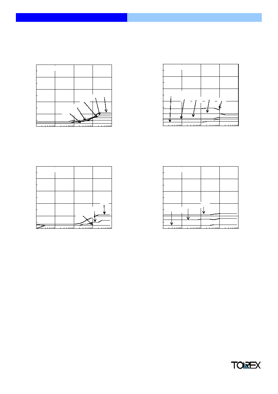
< 1ch Step-Down DC/DC Controller >
(1) Output Voltage vs. Output Current
* When setting V
OUT1
=1.0V, VIN=8.0V or 10.0V,
CL=94
µ
F (Tantalum) + 100
µ
F (OS Capacitor)
14
2ch. Step-Down / Inverting DCDC Controller ICs
XC9505 Series
FOSC=180kHz, V
OUT1
=5.0V
4.7
4.8
4.9
5.0
5.1
5.2
0.1
1
10
100
1000
Output Current1 I
OUT1
(mA)
Out
put
Volt
age1 V
OU
T1
(V)
PWM/PFM Switching Control
PWM Control
L1=47
µ
H(CDRH6D38), CL1=94
µ
F(Tantalum)
SD1:CMS02, Tr1:XP162A12A6P
VIN= 6.0V 8.0V 10V
FOSC=180kHz, V
OUT1
=1.0V
0.7
0.8
0.9
1.0
1.1
1.2
0.1
1
10
100
1000
Output Current1 I
OUT1
(mA)
Out
put
Volt
age1 V
OU
T1
(V)
PWM/PFM Switching Control
L1=47
µ
H(CDRH6D38), CL1=94
µ
F(Tantalum)
SD1:CMS02, Tr1:XP162A12A6P
10V
FOSC=180kHz, V
OUT1
=3.3V
3.0
3.1
3.2
3.3
3.4
3.5
0.1
1
10
100
1000
Output Current1 I
OUT1
(mA)
Out
put
Volt
age1 V
OU
T1
(V)
PWM/PFM Switching Control
PWM Control
L1=47
µ
H(CDRH6D38), CL1=94
µ
F(Tantalum)
SD1:CMS02, Tr1:XP162A12A6P
VIN=4.2V 5.0V 6.0V 8.0V 10V
FOSC=300kHz, V
OUT1
=1.0V
0.7
0.8
0.9
1.0
1.1
1.2
0.1
1
10
100
1000
Output Current1 I
OUT1
(mA)
Out
put
Volt
age1 V
OU
T1
(V)
PWM Control
VIN=2.7V 3.3V 4.2V 5.0V
6.0V 8.0V 10V
L1=22
µ
H(CDRH5D28), CL1=94
µ
F(Tantalum)
SD1:CMS02, Tr1:XP162A12A6P
FOSC=180kHz, V
OUT1
=1.0V
0.7
0.8
0.9
1.0
1.1
1.2
0.1
1
10
100
1000
Output Current1 I
OUT1
(mA)
Out
put
Volt
age1 V
OU
T1
(V)
PWM Control
L1=47
µ
H(CDRH6D38), CL1=94
µ
F(Tantalum)
SD1:CMS02, Tr1:XP162A12A6P
10V
VIN=2.7V 3.3V 4.2V
5.0V 6.0V 8.0V
4.2V 5.0V 6.0V 8.0V
VIN=2.7V 3.3V
FOCS=300kHz, V
OUT1
=1.0V
0.7
0.8
0.9
1.0
1.1
1.2
0.1
1
10
100
1000
Output Current1 I
OUT1
(mA)
Out
put
Volt
age1 V
OU
T1
(V)
PWM/PFM Switching Control
VIN=2.7V 3.3V
L1=22
µ
H(CDRH5D28), CL1=94
µ
F(Tantalum)
SD1:CMS02, Tr1:XP162A12A6P
5.0V
4.2V 6.0V 8.0V 10V

< 1ch Step-Down DC/DC Controller >
(1) Output Voltage vs. Output Current (Continued)
* When setting V
OUT1
=1.0V, VIN=8.0V or 10.0V,
CL=94
µ
F (Tantalum) + 100
µ
F (OS Capacitor)
15
XC9505 Series
2ch. Step-Down / Inverting DCDC Controller ICs
FOSC=300kHz, V
OUT1
=3.3V
3.0
3.1
3.2
3.3
3.4
3.5
0.1
1
10
100
1000
Output Current1 I
OUT1
(mA)
Out
put
Volt
age1 V
OU
T1
(V)
PWM Control
L1=22
µ
H(CDRH5D28), CL1=94
µ
F(Tantalum)
SD1:CMS02, Tr1:XP162A12A6P
10.0V
VIN=4.2V 5.0V 6.0V 8.0V
FOSC=300kHz, V
OUT1
=1.8V
1.5
1.6
1.7
1.8
1.9
2.0
0.1
1
10
100
1000
Output Current1 I
OUT1
(mA)
Out
put
Volt
age1 V
OU
T1
(V)
PWM Control
L1=22
µ
H(CDRH5D28), CL1=94
µ
F(Tantalum)
SD1:CMS02, Tr1:XP162A12A6P
VIN= 2.7V 3.3V 4.2V
5.0V 6.0V 8.0V 10V
FOSC=300kHz, V
OUT1
=1.8V
1.5
1.6
1.7
1.8
1.9
2.0
0.1
1
10
100
1000
Output Current1 I
OUT1
(mA)
Out
put
Volt
age1 V
OU
T1
(V)
PWM/PFM Switching Control
L1=22
µ
H(CDRH5D28), CL1=94
µ
F(Tantalum)
SD1:CMS02, Tr1:XP162A12A6P
VIN= 2.7V 3.3V 4.2V 5.0V
6.0V 8.0V 10V
FOSC=300kHz, V
OUT1
=2.5V
2.2
2.3
2.4
2.5
2.6
2.7
0.1
1
10
100
1000
Output Current1 I
OUT1
(mA)
Out
put
Volt
age1 V
OU
T1
(V)
PWM/PFM Switching Control
L1=22
µ
H(CDRH5D28), CL1=94
µ
F(Tantalum)
SD1:CMS02, Tr1:XP162A12A6P
10V
3.3V 4.2V 5.0V 6.0V
8.0V
VIN=2.7V
FOSC=300kHz, V
OUT1
=2.5V
2.2
2.3
2.4
2.5
2.6
2.7
0.1
1
10
100
1000
Output Current1 I
OUT1
(mA)
Out
put
Volt
age1 V
OU
T1
(V)
PWM Control
L1=22
µ
H(CDRH5D28), CL1=94
µ
F(Tantalum)
SD1:CMS02, Tr1:XP162A12A6P
10.0V
VIN= 2.7V 3.3V 4.2V
5.0V 6.0V 8.0V
FOSC=300kHz, V
OUT1
=3.3V
3.0
3.1
3.2
3.3
3.4
3.5
0.1
1
10
100
1000
Output Current1 I
OUT1
(mA)
Out
put
Volt
age1 V
OU
T1
(V)
PWM/PFM Switching Control
L1=22
µ
H(CDRH5D28), CL1=94
µ
F(Tantalum)
SD1:CMS02, Tr1:XP162A12A6P
10.0V
VIN=4.2V 5.0V 6.0V 8.0V

< 1ch Step-Down DC/DC Controller >
(1) Output Voltage vs. Output Current (Continued)
* When setting V
OUT1
=1.0V, VIN=8.0V or 10.0V,
CL=94
µ
F (Tantalum) + 100
µ
F (OS Capacitor)
16
XC9505 Series
2ch. Step-Down / Inverting DCDC Controller ICs
FOSC=500kHz, V
OUT1
=3.3V
3.0
3.1
3.2
3.3
3.4
3.5
0.1
1
10
100
1000
Output Current1 I
OUT1
(mA)
Out
put
Volt
age1 V
OU
T1
(V)
PWM Control
L1=10
µ
H(CDRH5D28), CL1=94
µ
F(Tantalum)
SD1:CMS02, Tr1:XP162A12A6P
VIN=4.2V 5.0V 6.0V 8.0V 10V
FOSC=500kHz, V
OUT1
=1.0V
0.7
0.8
0.9
1.0
1.1
1.2
0.1
1
10
100
1000
Output Current1 I
OUT1
(mA)
Out
put
Volt
age1 V
OU
T1
(V)
PWM Control
L1=10
µ
H(CDRH5D28), CL1=94
µ
F(Tantalum)
SD1:CMS02, Tr1:XP162A12A6P
VIN=2.7V 3.3V 4.2V 5.0V
6.0V 8.0V 10V
FOSC=500kHz, V
OUT1
=1.0V
0.7
0.8
0.9
1.0
1.1
1.2
0.1
1
10
100
1000
Output Current1 I
OUT1
(mA)
Out
put
Volt
age1 V
OU
T1
(V)
PWM/PFM Switching Control
L1=10
µ
H(CDRH5D28), CL1=94
µ
F(Tantalum)
SD1:CMS02, Tr1:XP162A12A6P
VIN=2.7V 3.3V 4.2V 5.0V
6.0V 8.0V 10V
FOSC=500kHz, V
OUT1
=3.3V
3.0
3.1
3.2
3.3
3.4
3.5
0.1
1
10
100
1000
Output Current1 I
OUT1
(mA)
Out
put
Volt
age1 V
OU
T1
(V)
PWM/PFM Switching Control
L1=10
µ
H(CDRH5D28), CL1=94
µ
F(Tantalum)
SD1:CMS02, Tr1:XP162A12A6P
VIN=4.2V 5.0V 6.0V 8.0V
10V
FOSC=300kHz, V
OUT1
=5.0V
4.7
4.8
4.9
5.0
5.1
5.2
0.1
1
10
100
1000
Output Current1 I
OUT1
(mA)
Out
put
Volt
age1 V
OU
T1
(V)
PWM Control
L1=22
µ
H(CDRH5D28), CL1=94
µ
F(Tantalum)
SD1:CMS02, Tr1:XP162A12A6P
10.0V
VIN= 6.0V 8.0V
FOSC=300kHz, V
OUT1
=5.0V
4.7
4.8
4.9
5.0
5.1
5.2
0.1
1
10
100
1000
Output Current1 I
OUT1
(mA)
Out
put
Volt
age1 V
OU
T1
(V)
PWM/PFM Switching Control
L1=22
µ
H(CDRH5D28), CL1=94
µ
F(Tantalum)
SD1:CMS02, Tr1:XP162A12A6P
10.0V
VIN= 6.0V 8.0V

< 1ch Step-Down DC/DC Controller >
(1) Output Voltage vs. Output Current (Continued)
* When setting V
OUT1
=1.0V, VIN=8.0V or 10.0V,
CL=94
µ
F (Tantalum) + 100
µ
F (OS Capacitor)
17
XC9505 Series
2ch. Step-Down / Inverting DCDC Controller ICs
FOSC=500kHz, V
OUT1
=5.0V
4.7
4.8
4.9
5.0
5.1
5.2
0.1
1
10
100
1000
Output Current1 I
OUT1
(mA)
Out
put
Volt
age1 V
OU
T1
(V)
PWM/PFM Switching Control
PWM Control
L1=10
µ
H(CDRH5D28), CL1=94
µ
F(Tantalum)
SD1:CMS02, Tr1:XP162A12A6P
VIN= 6.0V 8.0V 10V

< 1ch Step-Down DC/DC Controller >
(2) Efficiency vs. Output Current
* When setting V
OUT1
=1.0V, VIN=8.0V or 10.0V,
CL=94
µ
F (Tantalum) + 100
µ
F (OS Capacitor)
18
XC9505 Series
2ch. Step-Down / Inverting DCDC Controller ICs
FOSC=300kHz, V
OUT1
=1.0V
0
20
40
60
80
100
0.1
1
10
100
1000
Output Current1 I
OUT1
(mA)
E
ffi
ci
e
n
cy1
E
FFI1
(
%
)
L1=22
µ
H(CDRH5D28), CL1=94
µ
F(Tantalum)
SD1:CMS02, Tr1:XP162A12A6P
VIN=2.7V
4.2V
3.3V
PWM/PFM Switching Control
PWM Control
FOSC=300kHz, V
OUT1
=1.0V
0
20
40
60
80
100
0.1
1
10
100
1000
Output Current1 I
OUT1
(mA)
E
ffi
ci
e
n
cy1
E
FFI1
(
%
)
L1=22
µ
H(CDRH5D28), CL1=94
µ
F(Tantalum)
SD1:CMS02, Tr1:XP162A12A6P
8.0V
VIN=5.0V
10V
6.0V
PWM/PFM Switching Control
PWM Control
FOSC=180kHz, V
OUT1
=1.0V
0
20
40
60
80
100
0.1
1
10
100
1000
Output Current1 I
OUT1
(mA)
E
ffi
ci
e
n
cy1
E
FFI1
(
%
)
L1=47
µ
H(CDRH6D28), CL1=94
µ
F(Tantalum)
SD1:CMS02, Tr1:XP162A12A6P
VIN=2.7V
4.2V
3.3V
PWM/PFM Switching Control
PWM Control
FOSC=180kHz, V
OUT1
=3.3V
0
20
40
60
80
100
0.1
1
10
100
1000
Output Current1 I
OUT1
(mA)
E
ffi
ci
e
n
cy1
E
FFI1
(
%
)
L1=47
µ
H(CDRH6D28), CL1=94
µ
F(Tantalum)
SD1:CMS02, Tr1:XP162A12A6P
6.0V
VIN=4.2V
10V
8.0V
5.0V
PWM/PFM Switching Control
PWM Control
FOSC=180kHz, V
OUT1
=5.0V
0
20
40
60
80
100
0.1
1
10
100
1000
Output Current1 I
OUT1
(mA)
E
ffi
ci
e
n
cy1
E
FFI1
(
%
)
L1=47
µ
H(CDRH6D28), CL1=94
µ
F(Tantalum)
SD1:CMS02, Tr1:XP162A12A6P
8.0V
VIN=6.0V
10V
PWM/PFM Switching Control
PWM Control
FOSC=180kHz, V
OUT1
=1.0V
0
20
40
60
80
100
0.1
1
10
100
1000
Output Current1 I
OUT1
(mA)
E
ffi
ci
e
n
cy1
E
FFI1
(
%
)
L1=47
µ
H(CDRH6D28), CL1=94
µ
F(Tantalum)
SD1:CMS02, Tr1:XP162A12A6P
6.0V
VIN=5.0V
10V
8.0V
PWM/PFM Switching Control
PWM Control

< 1ch Step-Down DC/DC Controller >
(2) Efficiency vs. Output Current (Continued)
* When setting V
OUT1
=1.0V, VIN=8.0V or 10.0V,
CL=94
µ
F (Tantalum) + 100
µ
F (OS Capacitor)
19
XC9505 Series
2ch. Step-Down / Inverting DCDC Controller ICs
FOSC=300kHz, V
OUT1
=2.5V
0
20
40
60
80
100
0.1
1
10
100
1000
Output Current1 I
OUT1
(mA)
E
ffi
ci
e
n
cy1
E
FFI1
(
%
)
L1=22
µ
H(CDRH5D28), CL1=94
µ
F(Tantalum)
SD1:CMS02, Tr1:XP162A12A6P
4.2V
VIN=2.7V
3.3V
PWM/PFM Switching Control
PWM Control
FOSC=300kHz, V
OUT1
=1.8V
0
20
40
60
80
100
0.1
1
10
100
1000
Output Current1 I
OUT1
(mA)
E
ffi
ci
e
n
cy1
E
FFI1
(
%
)
L1=22
µ
H(CDRH5D28), CL1=94
µ
F(Tantalum)
SD1:CMS02, Tr1:XP162A12A6P
3.3V
VIN= 2.7V
4.2V
PWM/PFM Switching Control
PWM Control
FOSC=300kHz, V
OUT1
=2.5V
0
20
40
60
80
100
0.1
1
10
100
1000
Output Current1 I
OUT1
(mA)
E
ffi
ci
e
n
cy1
E
FFI1
(
%
)
L1=22
µ
H(CDRH5D28), CL1=94
µ
F(Tantalum)
SD1:CMS02, Tr1:XP162A12A6P
8.0V
VIN=5.0V
10V
6.0V
PWM/PFM Switching Control
PWM Control
FOSC=300kHz, V
OUT1
=1.8V
0
20
40
60
80
100
0.1
1
10
100
1000
Output Current1 I
OUT1
(mA)
E
ffi
ci
e
n
cy1
E
FFI1
(
%
)
L1=22
µ
H(CDRH5D28), CL1=94
µ
F(Tantalum)
SD1:CMS02, Tr1:XP162A12A6P
6.0V
VIN=5.0V
8.0V
10V
PWM/PFM Switching Control
PWM Control
FOSC=300kHz, V
OUT1
=3.3V
0
20
40
60
80
100
0.1
1
10
100
1000
Output Current1 I
OUT1
(mA)
E
ffi
ci
e
n
cy1
E
FFI1
(
%
)
L1=22
µ
H(CDRH5D28), CL1=94
µ
F(Tantalum)
SD1:CMS02, Tr1:XP162A12A6P
5.0V
VIN=4.2V
6.0V
10V
8.0V
PWM/PFM Switching Control
PWM Control
FOSC=300kHz, V
OUT1
=5.0V
0
20
40
60
80
100
0.1
1
10
100
1000
Output Current1 I
OUT1
(mA)
E
ffi
ci
e
n
cy1
E
FFI1
(
%
)
L1=22
µ
H(CDRH5D28), CL1=94
µ
F(Tantalum)
SD1:CMS02, Tr1:XP162A12A6P
8.0V
VIN=6.0V
10V
PWM/PFM Switching Control
PWM Control

< 1ch Step-Down DC/DC Controller >
(2) Efficiency vs. Output Current (Continued)
* When setting V
OUT1
=1.0V, VIN=8.0V or 10.0V,
CL=94
µ
F (Tantalum) + 100
µ
F (OS Capacitor)
20
XC9505 Series
2ch. Step-Down / Inverting DCDC Controller ICs
FOSC=500kHz, V
OUT1
=1.0V
0
20
40
60
80
100
0.1
1
10
100
1000
Output Current1 I
OUT1
(mA)
E
ffi
ci
e
n
cy1
E
FFI1
(
%
)
L1=10
µ
H(CDRH5D28), CL1=94
µ
F(Tantalum)
SD1:CMS02, Tr1:XP162A12A6P
4.2V
3.3V
VIN=2.7V
PWM/PFM Switching Control
PWM Control
FOSC=500kHz, V
OUT1
=3.3V
0
20
40
60
80
100
0.1
1
10
100
1000
Output Current1 I
OUT1
(mA)
E
ffi
ci
e
n
cy1
E
FFI1
(
%
)
L1=10
µ
H(CDRH5D28), CL1=94
µ
F(Tantalum)
SD1:CMS02, Tr1:XP162A12A6P
8.0V
VIN=6.0V
10V
FOSC=500kHz, V
OUT1
=1.0V
0
20
40
60
80
100
0.1
1
10
100
1000
Output Current1 I
OUT1
(mA)
E
ffi
ci
e
n
cy1
E
FFI1
(
%
)
L1=10
µ
H(CDRH5D28), CL1=94
µ
F(Tantalum)
SD1:CMS02, Tr1:XP162A12A6P
10V
VIN=5.0V
8.0V
6.0V
PWM/PFM Switching Control
PWM Control
FOSC=500kHz, V
OUT1
=3.3V
0
20
40
60
80
100
0.1
1
10
100
1000
Output Current1 I
OUT1
(mA)
E
ffi
ci
e
n
cy1
E
FFI1
(
%
)
L1=10
µ
H(CDRH5D28), CL1=94
µ
F(Tantalum)
SD1:CMS02, Tr1:XP162A12A6P
10V
VIN=4.2V
5.0V
6.0V
8.0V
PWM/PFM Switching Control
PWM Control
PWM/PFM Switching Control
PWM Control

< 1ch Step-Down DC/DC Controller >
(3) Ripple Voltage vs. Output Current
* When setting V
OUT1
=1.0V, VIN=8.0V or 10.0V,
CL=94
µ
F (Tantalum) + 100
µ
F (OS Capacitor)
21
XC9505 Series
2ch. Step-Down / Inverting DCDC Controller ICs
FOSC=180kHz, V
OUT1
=3.3V
0
20
40
60
80
100
0.1
1
10
100
1000
Output Current1 I
OUT1
(mA)
R
i
pple Volt
age1 (m
V)
PWM Control
L1=47
µ
H(CDRH6D28), CL1=94
µ
F(Tantalum)
SD1:CMS02, Tr1:XP162A12A6P
8.0V
VIN=4.2V 6.0V
10V
5.0V
FOSC=180kHz, V
OUT1
=3.3V
0
20
40
60
80
100
0.1
1
10
100
1000
Output Current1 I
OUT1
(mA)
R
i
pple Volt
age1 (m
V)
PWM/PFM Switching Control
L1=47
µ
H(CDRH6D28), CL1=94
µ
F(Tantalum)
SD1:CMS02, Tr1:XP162A12A6P
5.0V
VIN=4.2V
10V
8.0V
6.0V
FOSC=180kHz, V
OUT1
=5.0V
0
20
40
60
80
100
0.1
1
10
100
1000
Output Current1 I
OUT1
(mA)
R
i
pple Volt
age1 (m
V)
PWM Control
L1=47
µ
H(CDRH6D28), CL1=94
µ
F(Tantalum)
SD1:CMS02, Tr1:XP162A12A6P
10V
VIN=6.0V
8.0V
FOSC=180kHz, V
OUT1
=5.0V
0
20
40
60
80
100
0.1
1
10
100
1000
Output Current1 I
OUT1
(mA)
R
i
pple Volt
age1 (m
V)
PWM/PFM Switching Control
L1=47
µ
H(CDRH6D28), CL1=94
µ
F(Tantalum)
SD1:CMS02, Tr1:XP162A12A6P
10V
VIN=6.0V
8.0V
FOSC=180kHz, V
OUT1
=1.0V
0
20
40
60
80
100
0.1
1
10
100
1000
Output Current1 I
OUT1
(mA)
R
i
pple Volt
age1 (m
V)
VIN=2.7V
PWM/PFM Switching Control
L1=47
µ
H(CDRH6D28), CL1=94
µ
F(Tantalum)
SD1:CMS02, Tr1:XP162A12A6P
6.0V
10V
8.0V
5.0V
4.2V
3.3V
FOSC=180kHz, V
OUT1
=1.0V
0
20
40
60
80
100
0.1
1
10
100
1000
Output Current1 I
OUT1
(mA)
R
i
pple Volt
age1 (m
V)
PWM Control
L1=47
µ
H(CDRH6D28), CL1=94
µ
F(Tantalum)
SD1:CMS02, Tr1:XP162A12A6P
VIN=2.7V 3.3V 4.2V 5.0V
6.0V 8.0V 10V

< 1ch Step-Down DC/DC Controller >
(3) Ripple Voltage vs. Output Current (Continued)
* When setting V
OUT1
=1.0V, VIN=8.0V or 10.0V,
CL=94
µ
F (Tantalum) + 100
µ
F (OS Capacitor)
22
XC9505 Series
2ch. Step-Down / Inverting DCDC Controller ICs
FOSC=300kHz, V
OUT1
=1.8V
0
20
40
60
80
100
0.1
1
10
100
1000
Output Current1 I
OUT1
(mA)
R
i
pple Volt
age1 (m
V)
PWM/PFM Switching Control
L1=22
µ
H(CDRH5D28), CL1=94
µ
F(Tantalum)
SD1:CMS02, Tr1:XP162A12A6P
10V
VIN=2.7V
3.3V
4.2V
5.0V
6.0V
8.0V
FOSC=300kHz, V
OUT1
=1.8V
0
20
40
60
80
100
0.1
1
10
100
1000
Output Current1 I
OUT1
(mA)
R
i
pple Volt
age1 (m
V)
PWM Control
L1=22
µ
H(CDRH5D28), CL1=94
µ
F(Tantalum)
SD1:CMS02, Tr1:XP162A12A6P
VIN=2.7V 3.3V 4.2V 5.0V
6.0V 8.0V 10V
FOSC=300kHz, V
OUT1
=2.5V
0
20
40
60
80
100
0.1
1
10
100
1000
Output Current1 I
OUT1
(mA)
R
i
pple Volt
age1 (m
V)
PWM/PFM Switching Control
L1=22
µ
H(CDRH5D28), CL1=94
µ
F(Tantalum)
SD1:CMS02, Tr1:XP162A12A6P
5.0V
VIN=2.7V
3.3V
4.2V
6.0V
8.0V
10V
FOSC=300kHz, V
OUT1
=1.0V
0
20
40
60
80
100
0.1
1
10
100
1000
Output Current1 I
OUT1
(mA)
R
i
pple Volt
age1 (m
V)
PWM/PFM Switching Control
L1=22
µ
H(CDRH5D28), CL1=94
µ
F(Tantalum)
SD1:CMS02, Tr1:XP162A12A6P
5.0V
VIN=2.7V
3.3V
8.0V
4.2V
10V
6.0V
FOSC=300kHz, V
OUT1
=1.0V
0
20
40
60
80
100
0.1
1
10
100
1000
Output Current1 I
OUT1
(mA)
R
i
pple Volt
age1 (m
V)
PWM Control
L1=22
µ
H(CDRH5D28), CL1=94
µ
F(Tantaum)
SD1:CMS02, Tr1:XP162A12A6P
4.2V
8.0V 10V
VIN=2.7V 3.3V 5.0V 6.0V
FOSC=300kHz, V
OUT1
=2.5V
0
20
40
60
80
100
0.1
1
10
100
1000
Output Current1 I
OUT1
(mA)
R
i
pple Volt
age1 (m
V)
PWM Control
L1=22
µ
H(CDRH5D28), CL1=94
µ
F(Tantalum)
SD1:CMS02, Tr1:XP162A12A6P
VIN=2.7V 3.3V 4.2V 5.0V
6.0V 8.0V 10V

< 1ch Step-Down DC/DC Controller >
(3) Ripple Voltage vs. Output Current (Continued)
* When setting V
OUT1
=1.0V, VIN=8.0V or 10.0V,
CL=94
µ
F (Tantalum) + 100
µ
F (OS Capacitor)
23
XC9505 Series
2ch. Step-Down / Inverting DCDC Controller ICs
FOSC=300kHz, V
OUT1
=3.3V
0
20
40
60
80
100
0.1
1
10
100
1000
Output Current1 I
OUT1
(mA)
R
i
pple Volt
age1 (m
V)
PWM Control
L1=22
µ
H(CDRH5D28), CL1=94
µ
F(Tantalum)
SD1:CMS02, Tr1:XP162A12A6P
VIN=4.2V 5.0V 6.0V
8.0V 10V
FOSC=300kHz, V
OUT1
=3.3V
0
20
40
60
80
100
0.1
1
10
100
1000
Output Current1 I
OUT1
(mA)
R
i
pple Volt
age1 (m
V)
PWM/PFM Switching Control
L1=22
µ
H(CDRH5D28), CL1=94
µ
F(Tantalum)
SD1:CMS02, Tr1:XP162A12A6P
10.0V
VIN=4.2V
8.0V
6.0V
5.0V
FOSC=300kHz, V
OUT1
=5.0V
0
20
40
60
80
100
0.1
1
10
100
1000
Output Current1 I
OUT1
(mA)
R
i
pple Volt
age1 (m
V)
PWM Control
L1=22
µ
H(CDRH5D28), CL1=94
µ
F(Tantalum)
SD1:CMS02, Tr1:XP162A12A6P
10V
VIN=6.0V
8.0V
FOSC=300kHz, V
OUT1
=5.0V
0
20
40
60
80
100
0.1
1
10
100
1000
Output Current1 I
OUT1
(mA)
R
i
pple Volt
age1 (m
V)
PWM/PFM Switching Control
L1=22
µ
H(CDRH5D28), CL1=94
µ
F(Tantalum)
SD1:CMS02, Tr1:XP162A12A6P
10.0V
VIN=6.0V
8.0V
FOSC=500kHz, V
OUT1
=1.0V
0
20
40
60
80
100
0.1
1
10
100
1000
Output Current1 I
OUT1
(mA)
R
i
pple Volt
age1 (m
V)
PWM Control
L1=10
µ
H(CDRH5D28), CL1=94
µ
F(Tantalum)
SD1:CMS02, Tr1:XP162A12A6P
VIN=2.7V 3.3V 4.2V 5.0V
6.0V 8.0V 10V
FOSC=500kHz, V
OUT1
=1.0V
0
20
40
60
80
100
0.1
1
10
100
1000
Output Current1 I
OUT1
(mA)
R
i
pple Volt
age1 (m
V)
PWM/PFM Switching Control
L1=10
µ
H(CDRH5D28), CL1=94
µ
F(Tantalum)
SD1:CMS02, Tr1:XP162A12A6P
4.2V
6.0V
5.0V
10V
8.0V
VIN=2.7V
3.3V
< 1ch Step-Down DC/DC Controller >
(3) Ripple Voltage vs. Output Current (Continued)
* When setting V
OUT1
=1.0V, VIN=8.0V or 10.0V,
CL=94
µ
F (Tantalum) + 100
µ
F (OS Capacitor)
24
XC9505 Series
2ch. Step-Down / Inverting DCDC Controller Ics
FOSC=500kHz, V
OUT1
=3.3V
0
20
40
60
80
100
0.1
1
10
100
1000
Output Current1 I
OUT1
(mA)
R
i
pple Volt
age1 (m
V)
PWM Control
L1=10
µ
H(CDRH5D28), CL1=94
µ
F(Tantalum)
SD1:CMS02, Tr1:XP162A12A6P
10V
VIN=4.2V
5.0V
6.0V
8.0V
FOSC=500kHz, V
OUT1
=5.0V
0
20
40
60
80
100
0.1
1
10
100
1000
Output Current1 I
OUT1
(mA)
R
i
pple Volt
age1 (m
V)
PWM Control
L1=10
µ
H(CDRH5D28), CL1=94
µ
F(Tantalum)
SD1:CMS02, Tr1:XP162A12A6P
8.0V
VIN=6.0V
10V
FOSC=500kHz, V
OUT1
=5.0V
0
20
40
60
80
100
0.1
1
10
100
1000
Output Current1 I
OUT1
(mA)
R
i
pple Volt
age1 (m
V)
PWM/PFM Switching Control
L1=10
µ
H(CDRH5D28), CL1=94
µ
F(Tantalum)
SD1:CMS02, Tr1:XP162A12A6P
8.0V
VIN=6.0V
10V
FOSC=500kHz, V
OUT1
=3.3V
0
20
40
60
80
100
0.1
1
10
100
1000
Output Current1 I
OUT1
(mA)
R
i
pple Volt
age1 (m
V)
PWM/PFM Switching Control
L1=10
µ
H(CDRH5D28), CL1=94
µ
F(Tantalum)
SD1:CMS02, Tr1:XP162A12A6P
10V
VIN=4.2V
8.0V
6.0V
5.0V

Typical Performance Characteristics
< 2ch. Inverting DC/DC Controller >
(4) Output Voltage vs. Output Current
<Ceramic Capacitor and Compact Inductor use>
25
XC9505 Series
2ch. Step-Down / Inverting DC/DC Controller ICs
FOSC=300kHz, VOUT2= -7.5V
-7.8
-7.7
-7.6
-7.5
-7.4
-7.3
0.1
1
10
Output Current 2 IOUT2 (mA)
Out
put
Volt
age 2 VOU
T
2 (V)
VIN=2.7V 3.3V 4.2V 5.0V
L2=47
µ
H(LLB2520), CL2=10uF(ceramic)
SD2:CRS02, Tr2:XP152A12C0MR
PWM/PFM Switching Control
PWM Control
FOSC=180kHz, VOUT2= -7.5V
-7.8
-7.7
-7.6
-7.5
-7.4
-7.3
0.1
1
10
Output Current 2 IOUT2 (mA)
Out
put
Volt
age 2 VOU
T
2 (V)
VIN=2.7V 3.3V 4.2V 5.0V
L2=22
µ
H(LLB2520), CL2=10
µ
F(ceramic)
SD2:CRS02, Tr2:XP152A12C0MR
PWM/PFM Switching Control
PWM Control
FOSC=180kHz, VOUT2= -10.0V
-10.6
-10.4
-10.2
-10.0
-9.8
-9.6
0.1
1
10
Output Current 2 IOUT2 (mA)
Out
put
Volt
age 2 VOU
T
2 (V)
VIN=2.7V 3.3V 4.2V 5.0V
PWM/PFM Switching Control
PWM Control
L2=22uH(LLB2520), CL2=10uF(ceramic)
SD2:CRS02, Tr2:XP152A12C0MR

< 2ch. Inverting DC/DC Controller >
(4) Output Voltage vs. Output Current
<Ceramic Capacitor use>
26
XC9505 Series
2ch. Step-Down / Inverting DC/DC Controller ICs
FOSC=180kHz, VOUT2= -7.5V
-7.8
-7.7
-7.6
-7.5
-7.4
-7.3
0.1
1
10
100
Output Current 2 IOUT2 (mA)
Out
put
Volt
age 2 VOU
T
2 (V)
4.2V 5.0V
VIN=2.7V 3.3V
L2=22
µ
H(CDRH4D18C), CL2=10
µ
F(ceramic)
SD2:CRS02, Tr2:XP152A12C0MR
PWM/PFM Switching Control
PWM Control
FOSC=180kHz, VOUT2= -10.0V
-10.6
-10.4
-10.2
-10.0
-9.8
-9.6
0.1
1
10
100
Output Current 2 IOUT2 (mA)
Out
put
Volt
age 2 VOU
T
2 (V)
VIN=2.7V 3.3V 4.2V 5.0V
L2=15
µ
H(CDRH4D18C), CL2=10
µ
F(ceramic)
SD2:CRS02, Tr2:XP152A12C0MR
PWM/PFM Switching Control
PWM Control
FOSC=180kHz, VOUT2= -10.0V
-10.6
-10.4
-10.2
-10.0
-9.8
-9.6
0.1
1
10
100
Output Current 2 IOUT2 (mA)
Out
put
Volt
age 2 VOU
T
2 (V)
4.2V
VIN=2.7V 3.3V
L2=100
µ
H(CDRH4D18C), CL2=10
µ
F(ceramic)
SD2:CRS02, Tr2:XP152A12C0MR
5.0V
PWM/PFM Switching Control
PWM Control
FOSC=180kHz, VOUT2= -7.5V
-7.8
-7.7
-7.6
-7.5
-7.4
-7.3
0.1
1
10
100
Output Current 2 IOUT2 (mA)
Out
put
Volt
age 2 VOU
T
2 (V)
VIN=2.7V
L2=100
µ
H(CDRH4D18C), CL2=10
µ
F(ceramic)
SD2:CRS02, Tr2:XP152A12C0MR
4.2V
3.3V
5.0V
PWM/PFM Switching Control
PWM Control

< 2ch. Inverting DC/DC Controller >
(4) Output Voltage vs. Output Current
<Tantalum Capacitor use>
27
XC9505 Series
2ch. Step-Down / Inverting DC/DC Controller ICs
FOSC=180kHz, VOUT2= -7.5V
-7.8
-7.7
-7.6
-7.5
-7.4
-7.3
0.1
1
10
100
1000
Output Current 2 IOUT2 (mA)
Out
put
Volt
age 2 VOU
T
2 (V)
4.2V 5.0V
VIN=2.7V 3.3V
L2=22
µ
H(CDRH5D28), CL2=94
µ
F(Tantalum)
SD2:MA2Q737, Tr2:XP162A12A6P
PWM/PFM Switching Control
PWM Control
FOSC=180kHz, VOUT2= -10.0V
-10.6
-10.4
-10.2
-10.0
-9.8
-9.6
0.1
1
10
100
1000
Output Current 2 IOUT2 (mA)
Out
put
Volt
age 2 VOU
T
2 (V)
VIN=2.7V 3.3V 4.2V 5.0V
L2=22
µ
H(CDRH5D28), CL2=94
µ
F(Tantalum)
SD2:MA2Q737, Tr2:XP162A12A6P
PWM/PFM Switching Control
PWM Control
FOSC=300kHz, VOUT2= -5.0V
-5.3
-5.2
-5.1
-5.0
-4.9
-4.8
0.1
1
10
100
1000
Output Current 2 IOUT2 (mA)
Out
put
Volt
age 2 VOU
T
2 (V)
VIN=2.7V 3.3V
L2=15
µ
H(CDRH5D28), CL2=94
µ
F(Tantalum)
SD2:CRS02, Tr2:XP152A12C0MR
5.0V
PWM/PFM Switching Control
PWM Control
FOSC=300kHz, VOUT2= -7.5V
-7.8
-7.7
-7.6
-7.5
-7.4
-7.3
0.1
1
10
100
1000
Output Current 2 IOUT2 (mA)
Out
put
Volt
age 2 VOU
T
2 (V)
VIN=2.7V 3.3V
L2=15
µ
H(CDRH5D28), CL2=94
µ
F(Tantalum)
SD2:CRS02, Tr2:XP152A12C0MR
5.0V
PWM/PFM Switching Control
PWM Control
FOSC=300kHz, VOUT2= -10.0V
-10.6
-10.4
-10.2
-10.0
-9.8
-9.6
0.1
1
10
100
1000
Output Current 2 IOUT2 (mA)
Out
put
Volt
age 2 VOU
T
2 (V)
VIN=2.7V 3.3V 5.0V
L2=15
µ
H(CDRH5D28), CL2=94
µ
F(Tantalum)
SD2:CRS02, Tr2:XP152A12C0MR
PWM/PFM Switching Control
PWM Control
FOSC=300kHz, VOUT2= -15.0V
-15.6
-15.4
-15.2
-15.0
-14.8
-14.6
0.1
1
10
100
1000
Output Current 2 IOUT2 (mA)
Out
put
Volt
age 2 VOU
T
2 (V)
VIN=2.7V 3.3V
L2=15
µ
H(CDRH5D28), CL2=94
µ
F(Tantalum)
SD2:CRS02, Tr2:XP152A12C0MR
5.0V
PWM/PFM Switching Control
PWM Control

< 2ch. Inverting DC/DC Controller >
(5) Efficiency vs. Output Current
<Ceramic Capacitor and Compact Inductor use>
28
XC9505 Series
2ch. Step-Down / Inverting DC/DC Controller ICs
FOSC=180kHz, VOUT2= -7.5V
0
20
40
60
80
100
0.1
1
10
Output Current 2 IOUT2 (mA)
E
ffi
ci
e
n
cy2
E
FFI 2
(
%
)
3.3V
VIN=2.7V
4.2V
5.0V
L2=22
µ
H(LLB2520), C
L2
=10
µ
F(ceramic)
SD2:CRS02, Tr2:XP152A12C0MR
PWM/PFM Switching Control
PWM Control
FOSC=180kHz, VOUT2= -10.0V
0
20
40
60
80
100
0.1
1
10
Output Current 2 IOUT2 (mA)
E
ffi
ci
e
n
cy2
E
FFI 2
(
%
)
4.2V
VIN=2.7V
5.0V
3.3V
L2=22
µ
H(LLB2520), C
L2
=10
µ
F(ceramic)
SD2:CRS02, Tr2:XP152A12C0MR
PWM/PFM Switching Control
PWM Control
FOSC=300kHz, VOUT2= -7.5V
0
20
40
60
80
100
0.1
1
10
Output Current 2 IOUT2 (mA)
E
ffi
ci
e
n
cy2
E
FFI 2
(
%
)
3.3V
VIN=2.7V
5.0V
L2=47
µ
H(LLB2520), CL2=10
µ
F(ceramic)
SD2:CRS02, Tr2:XP152A12C0MR
PWM/PFM Switching Control
PWM Control

< 2ch. Inverting DC/DC Controller >
(5) Efficiency vs. Output Current (Continued)
<Ceramic Capacitor use>
29
XC9505 Series
2ch. Step-Down / Inverting DC/DC Controller ICs
FOSC=180kHz, VOUT2= -7.5V
0
20
40
60
80
100
0.1
1
10
100
Output Current 2 IOUT2 (mA)
E
ffi
ci
e
n
cy2
E
FFI 2
(
%
)
3.3V
VIN=2.7V
L2=100
µ
H(CDRH4D18C), CL2=10
µ
F(ceramic)
SD2:CRS02, Tr2:XP152A12C0MR
5.0V
4.2V
PWM/PFM Switching Control
PWM Control
FOSC=180kHz, VOUT2= -10.0V
0
20
40
60
80
100
0.1
1
10
100
Output Current 2 IOUT2 (mA)
E
ffi
ci
e
n
cy2
E
FFI 2
(
%
)
4.2V
VIN=2.7V
L2=100
µ
H(CDRH4D18C), CL2=10
µ
F(ceramic)
SD2:CRS02, Tr2:XP152A12C0MR
5.0V
3.3V
PWM/PFM Switching Control
PWM Control
FOSC=180kHz, VOUT2= -7.5V
0
20
40
60
80
100
0.1
1
10
100
Output Current 2 IOUT2 (mA)
E
ffi
ci
e
n
cy2
E
FFI 2
(
%
)
3.3V
VIN=2.7V
L2=22
µ
H(CDRH4D18C), CL2=10
µ
F(ceramic)
SD2:CRS02, Tr2:XP152A12C0MR
5.0V
4.2V
PWM/PFM Switching Control
PWM Control
FOSC=180kHz, VOUT2= -10.0V
0
20
40
60
80
100
0.1
1
10
100
Output Current 2 IOUT2 (mA)
E
ffi
ci
e
n
cy2
E
FFI 2
(
%
)
3.3V
VIN=2.7V
L2=15
µ
H(CDRH4D18C), CL2=10
µ
F(ceramic)
SD2:CRS02, Tr2:XP152A12C0MR
4.2V
5.0V
PWM/PFM Switching Control
PWM Control

< 2ch. Inverting DC/DC Controller >
(5) Efficiency vs. Output Current (Continued)
<Tantalum Capacitor use>
30
XC9505 Series
2ch. Step-Down / Inverting DC/DC Controller ICs
FOSC=180kHz, VOUT2= -7.5V
0
20
40
60
80
100
0.1
1
10
100
1000
Output Current 2 IOUT2 (mA)
E
ffi
ci
e
n
cy2
E
FFI 2
(
%
)
3.3V
VIN=2.7V
L2=22
µ
H(CDRH5D28), CL2=94
µ
F(Tantalum)
SD2:MA2Q737, Tr2:XP162A12A6P
5.0V
4.2V
PWM/PFM Switching Control
PWM Control
FOSC=300kHz, VOUT2= -10.0V
0
20
40
60
80
100
0.1
1
10
100
1000
Output Current 2 IOUT2 (mA)
E
ffi
ci
e
n
cy2
E
FFI 2
(
%
)
3.3V
VIN=2.7V
5.0V
L2=15
µ
H(CDRH5D28), CL2=94
µ
F(Tantalum)
SD2:CRS02, Tr2:XP152A12C0MR
PWM/PFM Switching Control
PWM Control
FOSC=180kHz, VOUT2= -10.0V
0
20
40
60
80
100
0.1
1
10
100
1000
Output Current 2 IOUT2 (mA)
E
ffi
ci
e
n
cy2
E
FFI 2
(
%
)
3.3V
VIN=2.7V
5.0V
4.2V
L2=22
µ
H(CDRH5D28), CL2=94
µ
F(Tantalum)
SD2:MA2Q737, Tr2:XP162A12A6P
PWM/PFM Switching Control
PWM Control
FOSC=300kHz, VOUT2= -5.0V
0
20
40
60
80
100
0.1
1
10
100
1000
Output Current 2 IOUT2 (mA)
E
ffi
ci
e
n
cy2
E
FFI 2
(
%
)
3.3V
VIN=2.7V
5.0V
L2=15
µ
H(CDRH5D28), CL2=94
µ
F(Tantalum)
SD2:CRS02, Tr2:XP152A12C0MR
PWM/PFM Switching Control
PWM Control
FOSC=300kHz, VOUT2= -7.5V
0
20
40
60
80
100
0.1
1
10
100
1000
Output Current 2 IOUT2 (mA)
E
ffi
ci
e
n
cy2
E
FFI 2
(
%
)
3.3V
VIN=2.7V
5.0V
L2=15
µ
H(CDRH5D28), CL2=94
µ
F(Tantalum)
SD2:CRS02, Tr2:XP152A12C0MR
PWM/PFM Switching Control
PWM Control
FOSC=300kHz, VOUT2= -15.0V
0
20
40
60
80
100
0.1
1
10
100
1000
Output Current 2 IOUT2 (mA)
E
ffi
ci
e
n
cy2
E
FFI 2
(
%
)
3.3V
VIN=2.7V
5.0V
L2=15
µ
H(CDRH5D28), CL2=94
µ
F(Tantalum)
SD2:CRS02, Tr2:XP152A12C0MR
PWM/PFM Switching Control
PWM Control

< 2ch. Inverting DC/DC Controller >
(6) Ripple Voltage vs. Output Current
<Ceramic Capacitor and Compact Inductor use>
31
XC9505 Series
2ch. Step-Down / Inverting DC/DC Controller ICs
FOSC=180kHz, VOUT2= -7.5V
0
20
40
60
80
100
0.1
1
10
Output Current 2 IOUT2 (mA)
R
i
pple Volt
age2 (m
V)
4.2V
VIN=2.7V
L2=22
µ
H(LLB2520), CL2=10
µ
F(ceramic)
SD2:CRS02, Tr2:XP152A12C0MR
5.0V
3.3V
FOSC=180kHz, VOUT2= -10.0V
0
20
40
60
80
100
0.1
1
10
Output Current 2 IOUT2 (mA)
R
i
pple Volt
age2 (m
V)
4.2V
VIN=2.7V
L2=22
µ
H(LLB2520), CL2=10
µ
F(ceramic)
SD2:CRS02, Tr2:XP152A12C0MR
5.0V
3.3V
PWM/PFM Switching Control
PWM Control
PWM/PFM Switching Control
PWM Control
FOSC=300kHz, VOUT2= -7.5V
0
20
40
60
80
100
0.1
1
10
Output Current 2 IOUT2 (mA)
R
i
pple Volt
age2 (m
V)
VIN=2.7V
3.3V
5.0V
L2=22
µ
H(LLB2520), C
L2
=10
µ
F(ceramic)
SD2:CRS02, Tr2:XP152A12C0MR
PWM/PFM Switching Control
PWM Control

< 2ch. Inverting DC/DC Controller >
(6) Ripple Voltage vs. Output Current (Continued)
<Ceramic Capacitor use>
32
XC9505 Series
2ch. Step-Down / Inverting DC/DC Controller ICs
FOSC=180kHz, VOUT2= -7.5V
0
20
40
60
80
100
0.1
1
10
100
Output Current 2 IOUT2 (mA)
R
i
pple Volt
age2 (m
V)
5.0V
VIN=2.7V
L2=22
µ
H(CDRH4D18C), CL2=10
µ
F(ceramic)
SD2:CRS02, Tr2:XP152A12C0MR
3.3V
4.2V
PWM/PFM Switching Control
PWM Control
FOSC=180kHz, VOUT2= -10.0V
0
20
40
60
80
100
0.1
1
10
100
Output Current 2 IOUT2 (mA)
R
i
pple Volt
age2 (m
V)
VIN=2.7V
L2=15
µ
H(CDRH4D18C), CL2=10
µ
F(ceramic)
SD2:CRS02, Tr2:XP152A12C0MR
4.2V
3.3V
PWM/PFM Switching Control
PWM Control
5.0V
FOSC=180kHz, VOUT2= -7.5V
0
20
40
60
80
100
0.1
1
10
100
Output Current 2 IOUT2 (mA)
R
i
pple Volt
age2 (m
V)
L2=100
µ
H(CDRH4D18C), CL2=10
µ
F(ceramic)
SD2:CRS02, Tr2:XP152A12C0MR
VIN=2.7V
3.3V
4.2V
5.0V
PWM/PFM Switching Control
PWM Control
FOSC=180kHz, VOUT2= -10.0V
0
20
40
60
80
100
0.1
1
10
100
Output Current 2 IOUT2 (mA)
R
i
pple Volt
age2 (m
V)
L2=100
µ
H(CDRH4D18C), CL2=10
µ
F(ceramic)
SD2:CRS02, Tr2:XP152A12C0MR
VIN=2.7V
3.3V
4.2V
5.0V
PWM/PFM Switching Control
PWM Control

< 2ch. Inverting DC/DC Controller >
(6) Ripple Voltage vs. Output Current (Continued)
<Tantalum Capacitor use>
33
XC9505 Series
2ch. Step-Down / Inverting DC/DC Controller ICs
FOSC=300kHz, VOUT2= -5.0V
0
20
40
60
80
100
0.1
1
10
100
1000
Output Current 2 IOUT2 (mA)
R
i
pple Volt
age2 (m
V)
3.3V
VIN=2.7V
5.0V
L2=15
µ
H(CDRH5D28), CL2=94
µ
F(Tantalum)
SD2:CRS02, Tr2:XP152A12C0MR
PWM/PFM Switching Control
PWM Control
FOSC=300kHz, VOUT2= -7.5V
0
20
40
60
80
100
0.1
1
10
100
1000
Output Current 2 IOUT2 (mA)
R
i
pple Volt
age2 (m
V)
VIN=2.7V
5.0V
L2=15
µ
H(CDRH5D28), CL2=94
µ
F(Tantalum)
SD2:CRS02, Tr2:XP152A12C0MR
PWM/PFM Switching Control
PWM Control
FOSC=180kHz, VOUT2= -15.0V
0
20
40
60
80
100
0.1
1
10
100
1000
Output Current 2 IOUT2 (mA)
R
i
pple Volt
age2 (m
V)
3.3V
VIN=2.7V
5.0V
L2=15
µ
H(CDRH5D28), CL2=94
µ
F(Tantalum)
SD2:CRS02, Tr2:XP152A12C0MR
PWM/PFM Switching Control
PWM Control
PWM/PFM Switching Control
PWM Control
FOSC=180kHz, VOUT2= -10.0V
0
20
40
60
80
100
0.1
1
10
100
1000
Output Current 2 IOUT2 (mA)
R
i
pple Volt
age2 (m
V)
4.2V
VIN=2.7V
L2=22
µ
H(CDRH5D28), CL2=94
µ
F(Tantalum)
SD2:MA2Q737, Tr2:XP162A12A6P
3.3V 5.0V
PWM/PFM Switching Control
PWM Control
FOSC=180kHz, VOUT2= -7.5V
0
20
40
60
80
100
0.1
1
10
100
1000
Output Current 2 IOUT2 (mA)
R
i
pple Volt
age2 (m
V)
4.2V
VIN=2.7V
L2=22
µ
H(CDRH5D28), CL2=94
µ
F(Tantalum)
SD2:MA2Q737, Tr2:XP162A12A6P
5.0V
3.3V
PWM/PFM Switching Control
PWM Control
3.3V
FOSC=300kHz, VOUT2= -10.0V
0
20
40
60
80
100
0.1
1
10
100
1000
Output Current 2 IOUT2 (mA)
R
i
pple Volt
age2 (m
V)
VIN=2.7V
5.0V
L2=15
µ
H(CDRH5D28), CL2=94
µ
F(Tantalum)
SD2:CRS02, Tr2:XP152A12C0MR
PWM/PFM Switching Control
PWM Control
3.3V

< 2ch. Inverting DC/DC Controller >
(7) Breakdown of Output Voltage
34
XC9505 Series
2ch. Step-Down / Inverting DC/DC Controller ICs
FOSC=300kHz,VIN= 3.3V
0
20
40
60
80
100
0.1
1
10
100
1000
Output Current 2 IOUT2 (mA)
E
ffi
ci
e
n
cy2
E
FFI 2
(
%
)
VOUT=-5.0V
-15.0V
-10.0V
-7.5V
PWM Control
L2=15
µ
H(CDRH5D28), CL2=94
µ
F(Tantalum)
SD2:MA2Q737,Tr2:XP162A12A6P
FOSC=500kHz,VIN= 3.3V
0
20
40
60
80
100
0.1
1
10
100
1000
Output Current 2 IOUT2 (mA)
E
ffi
ci
e
n
cy2
E
FFI 2
(
%
)
VOUT=-5.0V
-15.0V
-10.0V
-7.5V
PWM Control
L2=10
µ
H(CDRH5D28), CL2=94
µ
F(Tantalum)
SD2:MA2Q737,Tr2:XP162A12A6P
FOSC=300kHz,VIN= 3.3V
0
20
40
60
80
100
0.1
1
10
100
1000
Output Current 2 IOUT2 (mA)
R
i
pple Volt
age2 (m
V)
-7.5V
VOUT=-5.0V
L2=15
µ
H(CDRH5D28), CL2=94
µ
F(Tantalum)
SD2:MA2Q737, Tr2:XP162A12A6P
-15.0V
-10.0V
PWM Control
FOSC=500kHz,VIN= 3.3V
0
20
40
60
80
100
0.1
1
10
100
1000
Output Current 2 IOUT2 (mA)
R
i
pple Volt
age2 (m
V)
-7.5V
VOUT=-5.0V
L2=10
µ
H(CDRH5D28), CL2=94
µ
F(Tantalum)
SD2:MA2Q737, Tr2:XP162A12A6P
-15.0V
-10.0V
PWM Control
FOSC=300kHz,VIN= 3.3V
0
20
40
60
80
100
0.1
1
10
Output Current 2 IOUT2 (mA)
R
i
pple Volt
age2 (m
V)
L2=47
µ
H(LLB2520), CL2=10
µ
F(ceramic)
SD2:CRS02, Tr2:XP152A12C0MR
VOUT= - 5.0V
-7.5V
-10.0V
-15.0V
PWM/PFM Switching Control
PWM Control
FOSC=300kHz,VIN= 3.3V
0
20
40
60
80
100
0.1
1
10
Output Current 2 IOUT2 (mA)
E
ffi
ci
e
n
cy2
E
FFI 2
(
%
)
-7.5V
VOUT= -5.0V
-15.0V
-10.0V
L2=47
µ
H(LLB2520), CL2=10
µ
F(ceramic)
SD2:CRS02, Tr2:XP152A12C0MR
PWM/PFM Switching Control
PWM Control

< 2ch. Inverting DC/DC Controller >
(8) Breakdown of Coil Inductance Value
35
XC9505 Series
2ch. Step-Down / Inverting DC/DC Controller ICs
FOSC=300kHz,VIN3.3V,Output2= -7.5V
0
20
40
60
80
100
0.1
1
10
100
1000
Output Current 2 IOUT2 (mA)
E
ffi
ci
e
n
cy2
E
FFI 2
(
%
)
L=15u
47u
22uH
100uH
PWM Control
L2=CDRH5D28, CL2=94
µ
F(Tantalum)
SD2:MA2Q737, Tr2:XP162A12C0MR
FOSC=300kHz,VIN=3.3V,Output2= -7.5V
0
20
40
60
80
100
1
10
100
1000
Output Current 2 IOUT2 (mA)
R
i
pple Volt
age2 (m
V)
22u
L=15u
L2=CDRH5D28, CL2=94
µ
F(Tantalum)
SD2:MA2Q737, Tr2:XP162A12A6P
47uH
100uH
PWM Control

!
Typical Performacen Characteristics (Continued)
(9) Supply Current 1 vs. Supply Voltage
(10) Supply Current 1-1 vs. Supply Voltage
(11) Supply Current 1-2 vs. Supply Voltage
(12) Supply Current 1-3 vs. Supply Voltage
(13) Supply Current 1-4 vs. Supply Voltage
(14) Supply Current 2 vs. Supply Voltage
36
XC9505 Series
2ch. Step-Down / Inverting DC/DC Controller ICs
XC9505B092 (180KHz)
0
50
100
150
200
250
300
0
2
4
6
8
10
Supply Voltage VDD (V)
Supply
C
u
rrent
1 I
D
D
1
(µA)
Topr=85
o
C
25
o
C
-40
o
C
XC9505B092 (180KHz)
0
50
100
150
200
250
0
2
4
6
8
10
Supply Voltage VDD (V)
Supply
C
u
rrent
2 I
D
D
2
(µA)
XC9505B092 (180KHz)
0
50
100
150
200
250
300
0
2
4
6
8
10
Supply Current VDD (V)
Supply
C
u
rrent
1-4 I
D
D
1
-4 (µA)
XC9505B095 (180KHz)
0
50
100
150
200
250
0
2
4
6
8
10
Supply Voltage VDD (V)
Supply
C
u
rrent
1-3 I
D
D
1
-3 (µA)
XC9505B092 (180KHz)
0
50
100
150
200
250
0
2
4
6
8
10
Supply Voltage VDD (V)
Supply
C
u
rrent
1-2 I
D
D
1
-2 (µA)
XC9505B092 (180KHz)
0
50
100
150
200
0
2
4
6
8
10
Supply Voltage VDD (V)
Supply
C
u
rrent
1-1 I
D
D
1
-1 (µA)
Topr=85
o
C
25
o
C
-40
o
C
Topr=85
o
C
25
o
C
-40
o
C
Topr=85
o
C
25
o
C
-40
o
C
Topr=85
o
C
25
o
C
-40
o
C
Topr=85
o
C
25
o
C
-40
o
C

(15) Stand-by Current vs. Supply Voltage
(16) Oscillation Frequency vs. Supply Voltage
(17) PWM1, 2 'H''L' Voltage vs. Supply Voltage
(18) EN1, 2 'H''L' Voltage vs. Supply Voltage
(19) Maximum Duty Ratio 2 vs. Supply Voltage
(20) Soft-start Time vs. Supply Voltage
37
XC9505 Series
2ch. Step-Down / Inverting DC/DC Controller ICs
XC9505B092 (180kHz)
150
160
170
180
190
200
210
0
2
4
6
8
10
Supply Voltage VDD (V)
Os
c
illat
i
on F
r
equenc
y
F
o
s
c
(k
H
z
)
Topr=25
o
C
85
o
C
-40
o
C
XC9505B092 (180kHz)
0
2
4
6
8
10
0
2
4
6
8
10
Supply Voltage VDD (V)
St
and-by
C
u
rrent
I
S
T
B
(µA)
XC9505B092 (180kHz)
0
0.2
0.4
0.6
0.8
0
2
4
6
8
10
Supply Voltage VDD (V)
PW
M
1
,
2 'H
'' L' Volt
age
VPW
M
1
,
2
(V)
Topr=25
o
C
85
o
C
- 40
o
C
XC9505B092 (180KHz)
0
0.2
0.4
0.6
0.8
0
2
4
6
8
10
Supply Voltage VDD (V)
EN
1,
2 'H
'' L' Volt
age
VPW
M
1
,
2 (V)
- 40
o
C
85
o
C
Topr=25
o
C
XC9505B092 (180kHz)
0
5
10
15
20
25
0
2
4
6
8
10
Supply Voltage VDD (V)
S
o
ft-
sta
r
t
Ti
me
TS
S
1
(
m
se
c)
XC9505B092 (180kHz)
65
70
75
80
85
90
0
2
4
6
8
10
Supply Voltage VDD (V)
Ma
xi
mu
m Du
ty Ra
ti
o
2
Ma
xd
ty2
(%)
Topr=85
o
C
25
o
C
- 40
o
C
Topr=85
o
C
25
o
C
-40
o
C

(21) EXT1, 2 High ON Resistance vs. Supply Voltage
(22) EXT1, 2 Low ON Resistance vs. Supply Voltage
(23) Output Voltge vs. Ambient Temperature
(24) PFM Duty Ratio1, 2 vs. Supply Voltage
38
XC9505 Series
2ch. Step-Down / Inverting DC/DC Controller ICs
XC9505B092 (180kHz)
0
10
20
30
40
50
0
2
4
6
8
10
Supply Voltage VDD (V)
EXT
1,
2 H
ON
R
e
s
i
s
t
anc
e (
)
Topr=85
o
C
25
o
C
- 40
o
C
XC9505B092 (180kHz)
0
10
20
30
40
50
0
2
4
6
8
10
Supply Voltage VDD (V)
EXT
1,
2 L ON
R
e
s
i
s
t
anc
e (
)
Topr=85
o
C
25
o
C
- 40
o
C
XC9505B093(300kHz)
3.0
3.1
3.2
3.3
3.4
3.5
-50
-20
10
40
70
100
Ambient Temterature Ta (
0
C)
Out
put
Volt
age VOU
T
(V)
L=22uH(CDRH5D28), CL=94uF(Tantalum)
Tr:XP162A12A6, SD:CMS02
VIN=5.0V
IOUT=200mA
XC9505B092(180kHz)
20
25
30
35
40
0
2
4
6
8
10
Supply Voltage VDD (V)
P
F
M Du
ty Ra
ti
o
1
,
2
(
%
)
Topr=85
o
C
25
o
C
- 40
o
C

!
Load Transient Response
< 1 ch. Step-Up DC/DC Controller >
< VOUT1 = 3.3V, VIN = 5.0V
IOUT1 =100
µ
A
!
300mA >
"
PWM Control
"
PWM/PFM Switching Control
39
XC9505 Series
2ch. Step-Down / Inverting DC/DC Controller ICs
100µA
300mA
3.3V
CH1
CH2
200µsec/div
CH1:V
OUT1
, AC-COUPLED, 100mV/div
CH2:I
OUT1
, 150mA/div
FOSC=300kHz, V
OUT1
=3.3V
VIN=5.0V, I
OUT1
=100µA
300mA
100µA
300mA
3.3V
CH1
CH2
10msec/div
FOSC=300kHz, V
OUT1
=3.3V
VIN=5.0V, I
OUT1
=300mA
100µA
100µA
300mA
3.3V
CH1
CH2
10msec/div
100µA
300mA
3.3V
CH1
CH2
200µsec/div
FOSC=300kHz, V
OUT1
=3.3V
VIN=5.0V, I
OUT1
=100µA
300mA
FOSC=300kHz, V
OUT1
=3.3V
VIN=5.0V, I
OUT1
=300mA
100µA
CH1:V
OUT1
, AC-COUPLED, 50mV/div
CH2:I
OUT1
, 150mA/div
CH1:V
OUT1
, AC-COUPLED, 100mV/div
CH2:I
OUT1
, 150mA/div
CH1:V
OUT1
, AC-COUPLED, 100mV/div
CH2:I
OUT1
, 150mA/div

< 1 ch. Step-Up DC/DC Controller >
< VOUT1 = 3.3V, VIN = 5.0V
IOUT1 =10mA
!
300mA >
"
PWM Control
"
PWM/PFM Switching Control
40
XC9505 Series
2ch. Step-Down / Inverting DC/DC Controller ICs
300mA
3.3V
CH1
CH2
200µsec/div
10mA
300mA
3.3V
CH1
CH2
200µsec/div
10mA
300mA
3.3V
CH1
CH2
200µsec/div
10mA
300mA
3.3V
CH1
CH2
400µsec/div
10mA
FOSC=300kHz, V
OUT1
=3.3V
VIN=5.0V, I
OUT1
=10mA
300mA
FOSC=300kHz, V
OUT1
=3.3V
VIN=5.0V, I
OUT1
=10mA
300mA
FOSC=300kHz, V
OUT1
=3.3V
VIN=5.0V, I
OUT1
=300mA
10mA
FOSC=300kHz, V
OUT1
=3.3V
VIN=5.0V, I
OUT1
=300mA
10mA
CH1:V
OUT1
, AC-COUPLED, 50mV/div
CH2:I
OUT1
, 150mA/div
CH1:V
OUT1
, AC-COUPLED, 100mV/div
CH2:I
OUT1
, 150mA/div
CH1:V
OUT1
, AC-COUPLED, 50mV/div
CH2:I
OUT1
, 150mA/div
CH1:V
OUT1
, AC-COUPLED, 50mV/div
CH2:I
OUT1
, 150mA/div

< 1 ch. Step-Up DC/DC Controller >
< VOUT1 = 0.9V, VIN = 3.3V
IOUT1 =100
µ
A
!
300mA >
"
PWM Control
"
PWM/PFM Switching Control
41
XC9505 Series
2ch. Step-Down / Inverting DC/DC Controller ICs
100µA
300mA
0.9V
CH1
CH2
200µsec/div
100µA
300mA
0.9V
CH1
CH2
4msec/div
100µA
300mA
0.9V
CH1
CH2
4msec/div
100µA
300mA
0.9V
CH1
CH2
200µsec/div
CH1:V
OUT1
, AC-COUPLED, 20mV/div
CH2:I
OUT1
, 150mA/div
CH1:V
OUT1
, AC-COUPLED, 20mV/div
CH2:I
OUT1
, 150mA/div
CH1:V
OUT1
, AC-COUPLED, 20mV/div
CH2:I
OUT1
, 150mA/div
CH1:V
OUT1
, AC-COUPLED, 20mV/div
CH2:I
OUT1
, 150mA/div
FOSC=300kHz, V
OUT1
=0.9V
VIN=3.3V, I
OUT1
=100µA
300mA
FOSC=300kHz, V
OUT1
=0.9V
VIN=3.3V, I
OUT1
=100µA
300mA
FOSC=300kHz, V
OUT1
=0.9V
VIN=3.3V, I
OUT1
=300mA
100µA
FOSC=300kHz, V
OUT1
=0.9V
VIN=3.3V, I
OUT1
=300mA
100µA

< 1 ch. Step-Up DC/DC Controller >
< VOUT1 = 0.9V, VIN = 3.3V
IOUT1 =10mA
!
300mA >
"
PWM Control
"
PWM/PFM Switching Control
42
XC9505 Series
2ch. Step-Down / Inverting DC/DC Controller ICs
10mA
300mA
0.9V
CH1
CH2
200µsec/div
10mA
300mA
0.9V
CH1
CH2
200µsec/div
10mA
300mA
0.9V
CH1
CH2
100µsec/div
10mA
300mA
0.9V
CH1
CH2
100µsec/div
CH1:V
OUT1
, AC-COUPLED, 20mV/div
CH2:I
OUT1
, 150mA/div
CH1:V
OUT1
, AC-COUPLED, 20mV/div
CH2:I
OUT1
, 150mA/div
CH1:V
OUT1
, AC-COUPLED, 20mV/div
CH2:I
OUT
, 150mA/div
CH1:V
OUT1
, AC-COUPLED, 20mV/div
CH2:I
OUT1
, 150mA/div
FOSC=300kHz, V
OUT1
=0.9V
VIN=3.3V, I
OUT1
=10mA
300mA
FOSC=300kHz, V
OUT1
=0.9V
VIN=3.3V, I
OUT1
=10mA
300mA
FOSC=300kHz, V
OUT1
=0.9V
VIN=3.3V, I
OUT1
=300mA
10mA
FOSC=300kHz, V
OUT1
=0.9V
VIN=3.3V, I
OUT1
=300mA
10mA

< 1 ch. Step-Up DC/DC Controller >
< PWM Control
!
PWM / PFM Switching Control >
< Soft-Start Wave Form >
* EN2=GND
43
XC9505 Series
2ch. Step-Down / Inverting DC/DC Controller ICs
0.65V
3.3V
CH1
CH2
400µsec/div
CH1:V
OUT1
, AC-COUPLED ,10mV/div
CH2:PWM1 , 0.5V/div
0V
FOSC=300kHz, V
OUT1
=3.3V
VIN=5.0V, I
OUT1
=5mA PWM1 'L'
'H'
0.65V
3.3V
CH1
CH2
200µsec/div
0V
FOSC=300kHz, V
OUT1
=3.3V
VIN=5.0V, I
OUT1
=5A PWM1 'H'
'L'
CH1:V
OUT1
, AC-COUPLED ,20mV/div
CH2:PWM1, 0.5V/div
FOSC=300kHz, V
OUT1
=3.3V
VIN=5.0V, I
OUT1
=300mA
EN1 'L'
'H', CIN=47µF
CH1
CH2
CH3
3.3V
0.65V
200mA
4ms/div
CH1:V
OUT1
, 2.0V/div
CH2:I
IN1
, 100mA/div
CH3:EN1 , 0.5V/div
FOSC=300kHz, V
OUT1
=3.3V
VIN=5.0V, I
OUT1
=100mA
EN1 'L'
'H', CIN=47µF
CH1
CH2
CH3
3.3V
0.65V
75mA
4ms/div
CH1:V
OUT1
, 2.0V/div
CH2:I
IN1
, 50mA/div
CH3:EN1 , 0.5V/div

< 2 ch. Inverting DC/DC Controller >
< VOUT2 = - 7.5V, VIN = 3.3V
IOUT2 = - 100
µ
A
!
- 50mA >
(Tantalum Capacitor use)
!
PWM Control
!
PWM/PFM Switching Control
44
XC9505 Series
2ch. Step-Down / Inverting DC/DC Controller ICs
-100µA
-50mA
-7.5V
CH1
CH2
10msec/div
CH1:V
OUT2
, AC-COUPLED, 50mV/div
CH2:I
OUT2
, 50mA/div
FOSC=180kHz, V
OUT2
=-7.5V
VI
N=3.3V, I
OUT2
=-100µA
-50mA
-100µA
-50mA
-7.5V
CH1
CH2
200µsec/div
FOSC=180kHz, V
OUT2
=-7.5V
VIN=3.3V, I
OUT2
=-50mA
-100µA
-100µA
-50mA
-7.5V
CH1
CH2
200µsec/div
-100µA
-50mA
-7.5V
CH1
CH2
10msec/div
FOSC=180kHz, V
OUT2
=-7.5V
VIN=3.3V, I
OUT2
=-100µA
-50mA
FOSC=180kHz, V
OUT2
=-7.5V
VIN=3.3V, I
OUT2
=-50mA
-100µA
CH1:V
OUT2
, AC-COUPLED, 50mV/div
CH2:I
OUT2
, 50mA/div
CH1:V
OUT2
, AC-COUPLED, 50mV/div
CH2:I
OUT2
, 50mA/div
CH1:V
OUT2
, AC-COUPLED, 50mV/div
CH2:I
OUT2
, 50mA/div

< 2 ch. Inverting DC/DC Controller >
< VOUT2 = - 7.5V, VIN = 3.3V
IOUT2 = - 100
µ
A
!
- 20mA >
(Ceramic Capacitor use when coil current is discontinued.)
"
PWM Control
"
PWM/PFM Switching Control
45
XC9505 Series
2ch. Step-Down / Inverting DC/DC Controller ICs
-100µA
-20mA
-7.5V
CH1
CH2
1msec/div
CH1:V
OUT2
, AC-COUPLED, 20mV/div
CH2:I
OUT2
, 10mA/div
FOSC=180kHz, V
OUT2
=-7.5V
VIN=3.3V, I
OUT2
=-100µA
-20mA
-100µA
-20mA
-7.5V
CH1
CH2
200µsec/div
FOSC=180kHz, V
OUT2
=-7.5V
VIN=3.3V, I
OUT2
=-20mA
-100µA
-100µA
-20mA
-7.5V
CH1
CH2
200µsec/div
-100µA
-20mA
-7.5V
CH1
CH2
2msec/div
FOSC=180kHz, V
OUT2
=-7.5V
VIN=3.3V, I
OUT2
=-100µA
-20mA
FOSC=180kHz, V
OUT2
=-7.5V
VIN=3.3V, I
OUT2
=-20mA
-100µA
CH1:V
OUT2
, AC-COUPLED, 20mV/div
CH2:I
OUT2
, 10mA/div
CH1:V
OUT2
, AC-COUPLED, 50mV/div
CH2:I
OUT2
, 10mA/div
CH1:V
OUT2
, AC-COUPLED, 50mV/div
CH2:I
OUT2
, 10mA/div

< 2 ch. Inverting DC/DC Controller >
< VOUT2 = - 7.5V, VIN = 3.3V
IOUT2 = - 1mA
!
- 20mA >
"
PWM Control
"
PWM / PFM Switching Control
46
XC9505 Series
2ch. Step-Down / Inverting DC/DC Controller ICs
-1mA
-20mA
-7.5V
CH1
CH2
200µsec/div
CH1:V
OUT2
, AC-COUPLED, 20mV/div
CH2:I
OUT2
, 10mA/div
FOSC=180kHz, V
OUT2
=-7.5V
VIN=3.3V, I
OUT2
=-1mA
-20mA
-1mA
-20mA
-7.5V
CH1
CH2
200µsec/div
FOSC=180kHz, V
OUT2
=-7.5V
VIN=3.3V, I
OUT2
=-20mA
-1mA
-1mA
-20mA
-7.5V
CH1
CH2
400µsec/div
-1mA
-20mA
-7.5V
CH1
CH2
400µsec/div
FOSC=180kHz, V
OUT2
=-7.5V
VIN=3.3V, I
OUT2
=-1mA
-20mA
FOSC=180kHz, V
OUT2
=-7.5V
VIN=3.3V, I
OUT2
=-20mA
-1mA
CH1:V
OUT2
, AC-COUPLED, 20mV/div
CH2:I
OUT2
, 10mA/div
CH1:V
OUT2
, AC-COUPLED, 20mV/div
CH2:I
OUT2
, 10mA/div
CH1:V
OUT2
, AC-COUPLED, 20mV/div
CH2:I
OUT2
, 10mA/div

< 2 ch. Inverting DC/DC Controller >
< PWM Control
!
PWM / PFM Switching Control >
47
XC9505 Series
2ch. Step-Down / Inverting DC/DC Controller ICs
0.65V
-7.5V
CH1
CH2
200µsec/div
CH1:V
OUT2
, AC-COUPLED ,20mV/div
CH2:PWM
2
, 0.5V/div
0V
FOSC=180kHz, V
OUT2
=-7.5V
VIN=3.3V, I
OUT2
= - 5mA PWM2 'L'
"
'H'
0.65V
-7.5V
CH1
CH2
200µsec/div
0V
FOSC=180kHz, V
OUT2
=-7.5V
VIN=3.3V, I
OUT2
= - 5mA PWM2 'H'
"
'L'
CH1:VOUT
2
, AC-COUPLED ,20mV/div
CH2:PWM
2
, 0.5V/div