 | –≠–ª–µ–∫—Ç—Ä–æ–Ω–Ω—ã–π –∫–æ–º–ø–æ–Ω–µ–Ω—Ç: XC95093AR | –°–∫–∞—á–∞—Ç—å:  PDF PDF  ZIP ZIP |
September 30, 2003 Ver. 1
Synchronous Step-Down DC/DC Converter with Built-In LDO Regulator in Parallel plus Voltage Detector
!
Input Voltage Range
2.4V ~ 6.0V
"
APPLICATIONS
!
Output Voltage Range
DC/DC
0.9 ~ 4.0V (
±
2%)
#
HDD
VR
0.9 ~ 4.0V (
±
2%)
#
CD-R / RW, DVD
VD
0.9 ~ 5.0V (
±
2%)
#
PDAs, portable communication modem
!
Switching Frequency
300kHz, 600kHz, 1.2MHz
#
Cellular phones
!
Output Current
DC/DC
600mA
#
Palmtop computers
VR
200mA
#
Cameras, video recorders
!
Ultra Small Packages
MSOP-10, USP-10
!
Ceramic Capacitor Compatible
"
GENERAL DESCRIPTION
"
FEATURES
Input Voltage Range :
2.4V ~ 6.0V
Load Capacitors :
Ceramic Capacitors Compatible
(Low ESR Capacitors)
VD Function :
Sense internally either
VDD, DCOUT, or VROUT.
Nch Open Drain Output
<DC/DC Converter>
Output Voltage Range :
0.9 ~ 4.0V (
±
2%)
Output Current :
600mA
Controls :
PWM Control
Oscillation Frequency :
300kHz, 600kHz, 1.2MHz
<Regulator>
Output Voltage Range :
0.9 ~ 4.0V (
±
2%)
Current Limit
300mA
Dropout Voltage :
80mV @ IOUT=100mA (VOUT=2.8V)
High Ripple Rejection
60dB @1kHz (VOUT=2.8V)
"
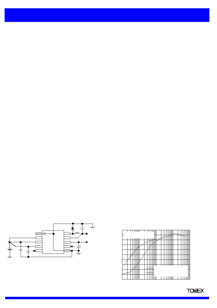
TYPICAL APPLICATION CIRCUIT
"
TYPICAL PERFORMANCE CHARACTERISTICS
XC9509 Series
PWM, PWM / PFM Automatic
Switching External
The XC9509 series consists of a step-down DC/DC converter and a
high-speed LDO regulator connected in parallel with the DC/DC
converter's output. A voltage detector is also built-in. Since the input
for the LDO voltage regulator block comes from the input power supply,
it is suited for use with various applications.
The DC/DC converter block incorporates a P-Channel driver transistor
and a synchronous N-Channel switching transistor. With an external
coil, diode and two capacitors, the XC9509 can deliver output currents
up to 600mA at efficiencies over 90%. The XC9509 is designed for
use with small ceramic capacitors.
A choice of three switching frequencies are available, 300 kHz,
600 kHz, and 1.2 MHz.
Output voltage settings for the DC/DC and VR are set-up internally in
0.1V steps within the range of 0.9V to 4.0V (
±
2.0%). For the VD, the
range is of 0.9V to 5.0V (
±
2.0%).
The soft start time of the series is internally set to 5ms. With the built-
in U.V.L.O. (Under Voltage Lock Out) function, the internal P-channel
driver transistor is forced OFF when input voltage becomes 1.4 V or
lower.
The functions of the MODE pin can be selected via the external control
pin to switch the DC/DC control mode and the disable pin to shut down
either the DC/DC block or the regulator block.
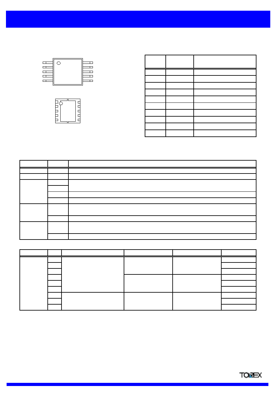
MSOP-10
(TOP VIEW)
LX
DCOUT
VROUT
MODE
AGND
PGND
CE
PVDD
AVDD
1
CL2
L
CL1
SD
( )
2
3
4
5
6
7
8
9
10
CIN2
VDOUT
VROUT
DCOUT
Semiconductor Ltd.
CIN1
XC9509Hxxxx
0
10
20
30
40
50
60
70
80
90
100
0.1
1
10
100
1000
DC/DC Output Current IDOUT (mA)
Ef
fi
c
i
e
n
c
y
EF
F
I
(%
)
PWM/PFM Switching Control
PWM Control
DC/DC Efficiency
(DCOUT:2.2V, 1.2MHz)
VIN=3.6V, Topr=25
O
C, L:4.7uH(CDRH4D28C)
CIN:4.7uF(ceramic), CL1:10uF(ceramic), CL2: 1uF(ceramic)
Data Sheet
1
Synchronous Step-Down DC/DC Converter with Built-In LDO Regulator in Parallel plus Voltage Detector
"
PIN CONFIGURATION
"
PIN ASSIGNMENT
1
2
3
4
5
6
7
8
9
10
"
SELECTION GUIDE
#
Ordering Information
XC9509
123456
The input for the voltage regulator block comes from VDD.
Control Methods, the MODE pin, the VD Sense pin (See the chart below)
Setting voltage and specifications of each DC/DC, VR, and VD (Based on the internal standard)
Oscillation Frequency of DC/DC :
300kHz
600kHz
1.2MHz
Package Type :
MSOP-10
USP-10
Device Orientation :
Embossed Tape : Standard Feed
Embossed Tape : Reverse Feed
%
Control Methods, MODE Pins, and VD SENSE Pins
* The XC9509A to F series' MODE pin switches either the regulator block or DC/DC block to stand-by mode.
When the CE mode is off, every function except for the VD function enters into stand-by mode.
(The MODE pin does not operate independently.)
PWM Control
PFM/PWM Auto Switch
PWM Control
VDD
DCOUT
VROUT
DC/DC : OFF
DC/DC : ON
VDD
DCOUT
VROUT
VDD
DCOUT
VROUT
H
K
PWM, PFM/PWM Manual Switch
XC9509 Series
VD SENSE
VR : OFF
VR : ON
SERIES
XC9509
A
1
L
B
C
D
E
F
PIN
NUMBER
FUNCTION
PIN NAME
Power Ground
PGND
VROUT
A
D
VR Output
Switch
LX
DCOUT
DC/DC Output
MODE
CE
PVDD
VDOUT
AVDD
AGND
Mode Switch
Chip Enable
Power Supply 1
VD Input
Power Supply 2
Analog Ground
1
23
DESIGNATOR
DESCRIPTION
SYMBOL
R
L
6
5
4
3
6
C
DC/DC CONTROL METHODS
MODE PINS (H LEVEL)
MODE PINS (L LEVEL)
Semiconductor Ltd.
PGND 1
CE 2
PVDD 3
AVDD 4
VDOUT 5
10 LX
9 DCOUT
8 VROUT
7 MODE
6 AGND
MSOP-10 (TOP VIEW)
USP-10 (TOP VIEW)
PGND 1
CE 2
PVDD 3
AVDD 4
VDOUT 5
10 LX
9 DCOUT
8 VROUT
7 MODE
6 AGND
Data Sheet
2

Synchronous Step-Down DC/DC Converter with Built-In LDO Regulator in Parallel plus Voltage Detector
"
PACKAGING INFORMATION
%
MSOP-10
%
USP-10
"
BLOCK DIAGRAM
* Diodes shown in the above circuits are protective diodes.
"
ABSOLUTE MAXIMUM RATINGS
Ta=25
O
C
(*1) IOUT = Pd / (VIN - VOUT) when PC board mounting.
(*2) Package power dissipation
V
VDOUT
CE Pin Voltage
MODE Pin Voltage
USP-10
MSOP-10
MODE
- 0.3 ~ VDD + 0.3
- 0.3 ~ VDD + 0.3
V
DCOUT
- 0.3 ~ VDD + 0.3
V
PVDD
V
CE
- 0.3 ~ VDD + 0.3
SYMBOL
RATINGS
UNITS
AVDD
- 0.3 ~ 6.5
V
- 0.3 ~ VDD + 0.3
V
- 55 ~ + 125
O
C
O
C
120 (*2)
Topr
Tstg
Storage Temperature Range
VDOUT Pin Voltage
LX Pin Voltage
Continuous Power Dissipation (*1)
Operating Temperature Range
VROUT Pin Voltage
AVDD Pin Voltage
PVDD Pin Voltage
DCOUT Pin Voltage
PARAMETER
350
Pd
XC9509 Series
mW
LX
VROUT
- 0.3 ~ VDD + 0.3
V
- 0.3 ~ VDD + 0.3
V
- 40 ~ + 85
0.15+0.01
0.
53+
0
.10
0~5
O
-
-
3.00+0.10
3.00+0.
1
0
4.90+0.
1
0
-
-
-
0.
8
6
+
0
.
0
5
0
.0
7
5
+
0
.0
2
5
(0.5
)
(0.2)
-
-
2.7+0.05
2.
6+
0.
06
M
AX 0.
6
0.30
0.15
0.
25+
0.
0
6
(0
.
1
)
(
1
.
50)
2.30
(0.5)
0.2+0.05
* Soldering fillet surface is not formed
because the sides of the pins are not
plated.
Semiconductor Ltd.
+
-
Vref with
soft start
PWM/PFM
Controller
Phase
Compensation
+
-
Logic
Buffer,
Driver
Current Limit &
Feedback
R amp Wave
Generator,
OSC
DCOUT
AVDD
-
+
U.V.L.O
LX
VROUT
AGND
+
-
Current
Li mi t
Vref
MODE
MODE
CONTROL
eac h
circuit
+
-
VDOUT
PGND
CE
ON/OFF,
CONTROL
eac h
circuit
Vref
PVDD
SENSE
(VDD or DCOUT or VROUT)
Data Sheet
3

Synchronous Step-Down DC/DC Converter with Built-In LDO Regulator in Parallel plus Voltage Detector
"
ELECTRICAL CHARACTERISTICS
XC9509HxxCAx
%
Common Characteristics
%
DC/DC Converter (2.2V product)
%
Regulator (1.8V product)
VMH
IROUT=30mA
IDOUT=30mA
-40
O
C<Topr<85
O
C
MODE 'H' Level Voltage
0.6
Connected to the external components,
IDOUT=10mA
-
1
IMH
- 0.1
Connected to the external components,
IDOUT=30mA
1
V
3
IDD2
3
MODE 'L' Level Current
µ
IML
- 0.1
-
MODE 'H' Level Current
MODE 'L' Level Voltage
VML
VSS
- 0.1
CONDITIONS
µ
-
0.25
V
0.1
µ
Ta=25
O
C
1
0.1
2
Ta=25
O
C
mA
3
mV
7
7
2
ppm
/
O
C
V
2
- 0.1
-
0.1
21
UNITS
mA
-
3
-
-
0.25
-
VDD
0.1
-
1.2
-
38
30
CE 'L' Level Voltage
VCEL
VSS
3
VDD
µ
1
V
1
3
V
1.40
2.5
-
µ
-
6.0
1.78
Supply Current 2
-
µ
1
300
-
µ
1
-
240
PARAMETER
SYMBOL
MIN.
IDD1
VIN=CE=DCOUT=5.0V
MAX.
UNITS
TEST CIRCUIT
V
3
mA
2
mS
VROUT=VSS
VIN={VOUT(T) + 1.0} VDC + 0.5Vp-pAC
IROUT=30mA, f=1kHz
-
60
2
6
-
0.5
-
5
3
-
-
-
-
MAX.
3
TYP.
±
100
3
TEST CIRCUIT
PFM Duty Ratio
CONDITIONS
%
UNITS
-
%
0
%
-
Connected to the external components,
No Load
DCOUT=VIN
TEST CIRCUIT
2.156
2.200
2.244
V
3
MIN.
TYP.
MAX.
Manimum Duty Ratio
MINDUTY
3
4
MAXDUTY
1.02
Oscillation Frequency
FOSC
Maximum Duty Ratio
DCOUT=0V
PFMDUTY
3
1.20
1.38
MHz
100
-
-
-
4
RLXL
LX SW 'High' On Resistance
(note 3)
RLXH
-
DCOUT=0V, LX=VIN-0.05V
0.5
600
%
Connected to the external components,
IDOUT=100mA
-
90
-
A
-
Efficiency (note 4)
EFFI
Temperature Characteristics
!
Topr
#
VOUT
Output Voltage
!
VOUT
TSS
-
PARAMETER
SYMBOL
MIN.
Connected to the external components,
CE=0V
"
VIN, IDOUT=1mA
Latch Time (note 5)
Tlat
CONDITIONS
%/V
2
Maximum Output Current
IMAX2
200
-
Load Regulation
!
VROUT
Dropout Voltage 1 (note 6)
Vdif 1
mV
2
15
50
mV
2
30
-
-
85
-
0.6
Current Limit
Line Regulation
ILIM2
Output Voltage
VROUT(E)
CE 'H' Level Current
ICEH
!
VOUT
Soft Start Time
Stand-by Current (note 1)
ISTB
CE 'H' Level Voltage
VCEH
VIN
Input Voltage Range
VUVLO
U.V.L.O. Voltage (note 2)
Supply Current 1
XC9509 Series
Ta=25
O
C
TYP.
VIN=CE=5.0V, DCOUT=0V
V
-
0.6
-
-
VIN=6.5V, CE=0V
1.00
2.4
ILIM1
Current Limit
PARAMETER
Output Voltage
SYMBOL
DCOUT
Maximum Output Current
IMAX1
LX SW 'Low' On Resistance
CE 'L' Level Current
ICEL
IDOUT=30mA
-40
O
C<Topr<85
O
C
mS
-
ppm
/
O
C
5
Connected to the external components,
VIN=CE=5.0V,
Short DCOUT by 1
resistor
-
8
1.800
1.764
1.836
1mA<IROUT<100mA
IROUT=30mA
IROUT=100mA
-
-
-
dB
VROUT(T)+1V<VIN<6V
VROUT=VROUT(E)x0.9
-
-
mA
300
-
-
0.2
PSRR
!
VOUT
-
-
-
±
100
IROUT=30mA
!
VIN
#
VOUT
30
Ripple Rejection Rate
Dropout Voltage 2
Vdif 2
Short-Circuit Current
ISHORT
-
Temperature Characteristics
!
Topr
#
VOUT
Output Voltage
Semiconductor Ltd.
Data Sheet
4

Synchronous Step-Down DC/DC Converter with Built-In LDO Regulator in Parallel plus Voltage Detector
"
ELECTRICAL CHARACTERISTICS (Continued)
%
Detector (2.7V product)
Test Conditions :
Unless otherwise stated;
* VROUT(T) : Setting Output Voltage
DC/DC : VIN=3.6V [@ DCOUT:2.2V]
VD : VIN=6.0V
VR : VIN = VROUT(T) + 1.0 (V) [When VROUT(T) <1.4V, VIN =2.4V]
note 1 : VD operates when in stand-by mode.
note 2 : Including hysteresis operating voltage range.
note 3 : On resistance = 0.05V / ILX
note 4 : EFFI = { ( Output Voltage x Output Current ) / ( Input Voltage x Input Current) } x 100
note 5 : Time until it short-circuits DCOUT with GND through 1
of resistance from a state of operation
and is set to DCOUT=0V from current limit pulse generating.
note 6 : Vdif = (VIN1
(note 7)
- VROUT1
(note 8 )
)
note 7 : VIN 1 = The input voltage when VROUT1 appears as input voltage is gradually decreased.
note 8 : VROUT1 = A voltage equal to 98% of the output voltage whenever an amply stabilized IOUT {VROUT(T) + 1.0V} is input.
Temperature Characteristics
!
Topr
#
VDF
8
-
-40
O
C<Topr<85
O
C
±
100
-
ppm
/
O
C
Output Voltage
!
VDF
%
-
5
8
2.646
2.754
Hysteresis Range
VHYS
3
TEST CIRCUIT
V
8
Detect Voltage
VDF
2.700
VDOUT=0.5V
VD Output Current
IVD
1
UNITS
XC9509 Series
CONDITIONS
Ta=25
O
C
PARAMETER
SYMBOL
TYP.
MAX.
MIN.
-
-
mA
9
Semiconductor Ltd.
Data Sheet
5