
XP152A12C0MR
Power MOS FET
474
u
P-Channel Power MOS FET
Applications
DMOS Structure
Notebook PCs
Low On-State Resistance : 0.3
(max)
Cellular and portable phones
Ultra High-Speed Switching
On - board power supplies
Gate Protect Diode Built-in
Li - ion battery systems
SOT - 23 Package
General Description
Features
The XP152A12C0MR is a P-Channel Power MOS FET with low on-state
Low on-state resistance : Rds (on) = 0.3
( Vgs = -4.5V )
resistance and ultra high-speed switching characteristics.
Rds (on) = 0.5
( Vgs = -2.5V )
Because high-speed switching is possible, the IC can be efficiently
Ultra high-speed switching
set thereby saving energy.
Gate Protect Diode Built-in
In order to counter static, a gate protect diode is built-in.
Operational Voltage : -2.5V
The small SOT-23 package makes high density mounting possible.
High density mounting : SOT - 23
Pin Configuration
Pin Assignment
PIN NUMBER
PIN NAME
G
Gate
S
Source
D
Drain
Equivalent Circuit
Absolute Maximum Ratings
Ta=25
O
C
SYMBOL
RATINGS
UNITS
Vdss
-20V
Vgss
+ 12
V
Id
-0.7
A
Idp
-2.8
A
Idr
-0.7
A
Pd
0.5
W
Tch
150
O
C
Tstg
-55 to 150
O
C
P - Channel MOS FET
( 1 device built-in )
( note ) : When implemented on a ceramic PCB
Storage Temperature
Reverse Drain Current
Continuous Channel
Power Dissipation (note)
Channel Temperature
Drain - Source Voltage
Gate - Source Voltage
Drain Current (DC)
Drain Current (Pulse)
FUNCTION
2
PARAMETER
1
3
SOT - 23 Top View
1
2
3
G
D
S
1
2
3

475
u
Electrical Characteristics
DC characteristics
Ta=25
�
C
PARAMETER
SYMBOL
CONDITIONS
MIN
TYP
MAX
UNITS
Drain Cut-off Current
Idss
Vds = - 20 , Vgs = 0V
- 10
�
A
Gate-Source Leakage Current
Igss
Vgs =
�
12 , Vds = 0V
�
10
�
A
Gate-Source Cut-off Voltage
Vgs (off )
Id = -1mA , Vds = - 10V
- 0.5
- 1.2
V
Drain-Source On-state Resistance
Id = - 0.4A , Vgs = - 4.5V
0.23
0.3
( note )
Id = - 0.4A , Vgs = - 2.5V
0.37
0.5
Forward Transfer Admittance
( note )
Body Drain Diode
Forward Voltage
( note ) : Effective during pulse test.
Dynamic characteristics
Ta=25
�
C
PARAMETER
SYMBOL
CONDITIONS
MIN
TYP
MAX
UNITS
Input Capacitance
Ciss
180pF
Output Capacitance
Coss
Vds = - 10V , Vgs = 0V
120
pF
Feedback Capacitance
Crss
f = 1 MHz
60pF
Switching characteristics
Ta=25
�
C
PARAMETER
SYMBOL
CONDITIONS
MIN
TYP
MAX
UNITS
Turn-on Delay Time
td ( on )
5
ns
Rise Time
tr
Vgs = - 5V , Id = - 0.4A
20
ns
Turn-off Delay Time
td ( off )
Vdd = - 10V
55
ns
Fall Time
tf
70ns
Thermal characteristics
PARAMETER
SYMBOL
CONDITIONS
MIN
TYP
MAX
UNITS
Thermal Resistance
Implement on a ceramic
( channel - surroundings )
PCB
�
C / W
250
Rth ( ch - a )
Vf
If = - 0.7A , Vgs = 0V
V
-0.8
- 1.1
Id = - 0.4A , Vds = - 10V
| Yfs |
Rds ( on )
S
1.5
XP152A12C0MR
Power MOS FET
476
u
-3
-2.5
-2
-1.5
-1
-0.5
0
-3
-2.5
-2
-1.5
-1
-0.5
0
Ta=25, Pulse Test
-2V
-2.5V
-3V
-4.5V
-4V
-5V
-3.5V
-3
-2.5
-2
-1.5
-1
-0.5
0
-3
-2.5
-2
-1.5
-1
-0.5
0
125
25
0
0.2
0.4
0.6
0.8
-10
-8
-6
-4
-2
0
Ta=25, Pulse Test
-0.4A
0.1
1
-3
-2.5
-2
-1.5
-1
-0.5
0
Vgs=-2.5V
-4.5V
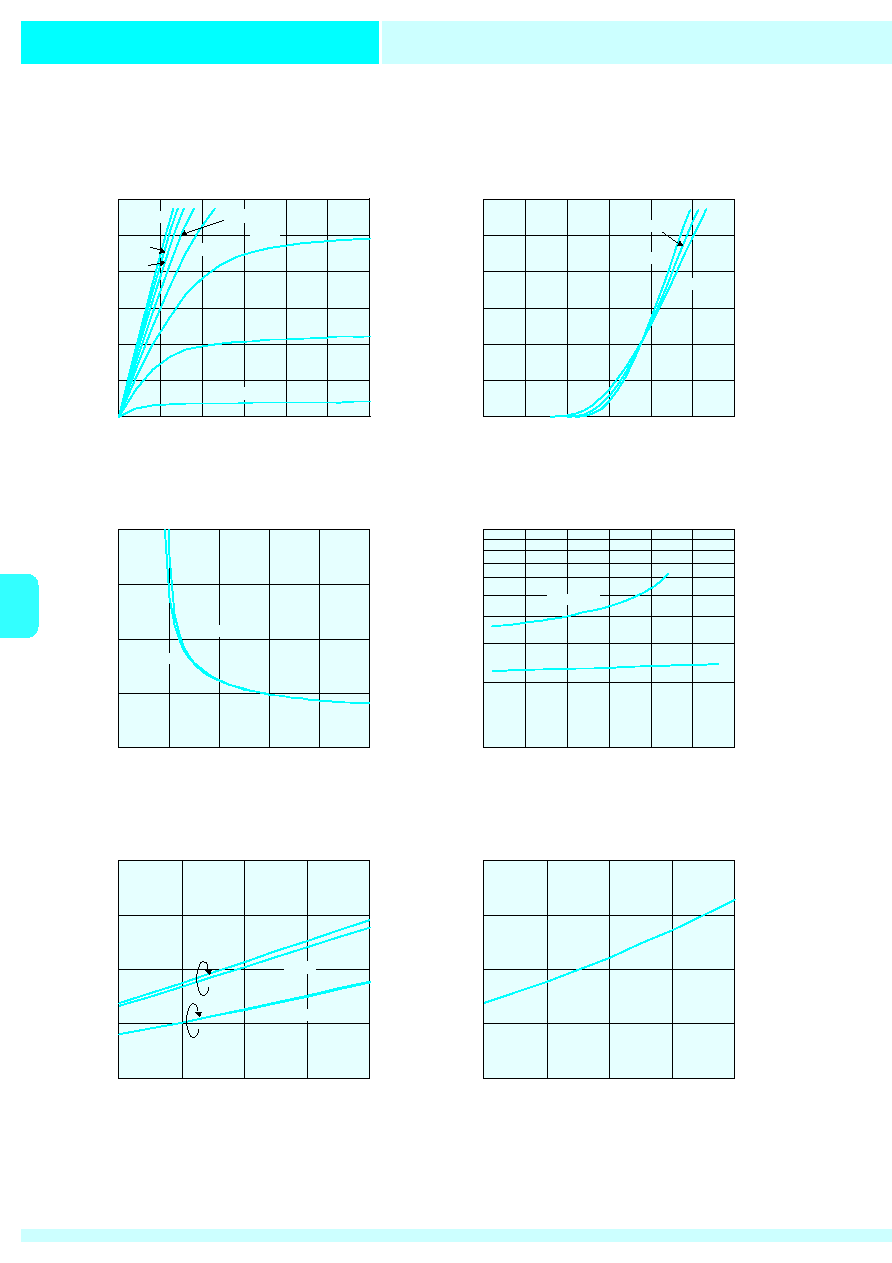
Electrical Characteristics
Drain Current vs. Drain/Source Voltage
Drain Current vs. Gate/Source Voltage
Drain/Source On State Resistance vs. Drain Current
Drain/Source On State Resistance vs. Gate/Source Voltage
Drain/Source Voltage:Vds (V)
Gate/Source Voltage:Vgs (V)
Drain Current:Id (A)
Drain Current:Id (A)
Vds=-10V, Pulse Test
Ta=25, Pulse Test
Drain/Source On State Resistance
:Rds (on) ()
Drain/Source On State Resistance
:Rds (on) ()
Gate/Source Voltage:Vgs (V)
Drain Current:Id (A)
Id=-0.7A
Ta=-55
Vgs=-1.5V
0
0.2
0.4
0.6
0.8
-50
0
50
100
150
-4.5V
-0.4A, -0.7A
-0.4
-0.2
0
0.2
0.4
-50
0
50
100
150
Vgs=-2.5V
Pulse Test
Id=-0.7A
-0.4A
Gate/Source Cut-Off Voltage Variance
:Vgs(off) Variance (V)
Vds=-10V, Id=-1mA
Gate/Source Cut off Voltage Variance vs. Ambient Temperature
Ambient Temp.:Topr ()
Ambient Temp.:Topr ()
Drain/Source On State Resistance
:Rds (on) ()
Drain/Source On State Resistance vs. Ambient Temperature
477
u
10
100
1000
-20
-15
-10
-5
0
Vgs=0V, f=1MHz, Ta=25
Capacitance:C (pF)
Coss
Ciss
Crss
1
10
100
1000
10000
-2
-1.5
-1
-0.5
0
tr
td(on)
td(off)
tf
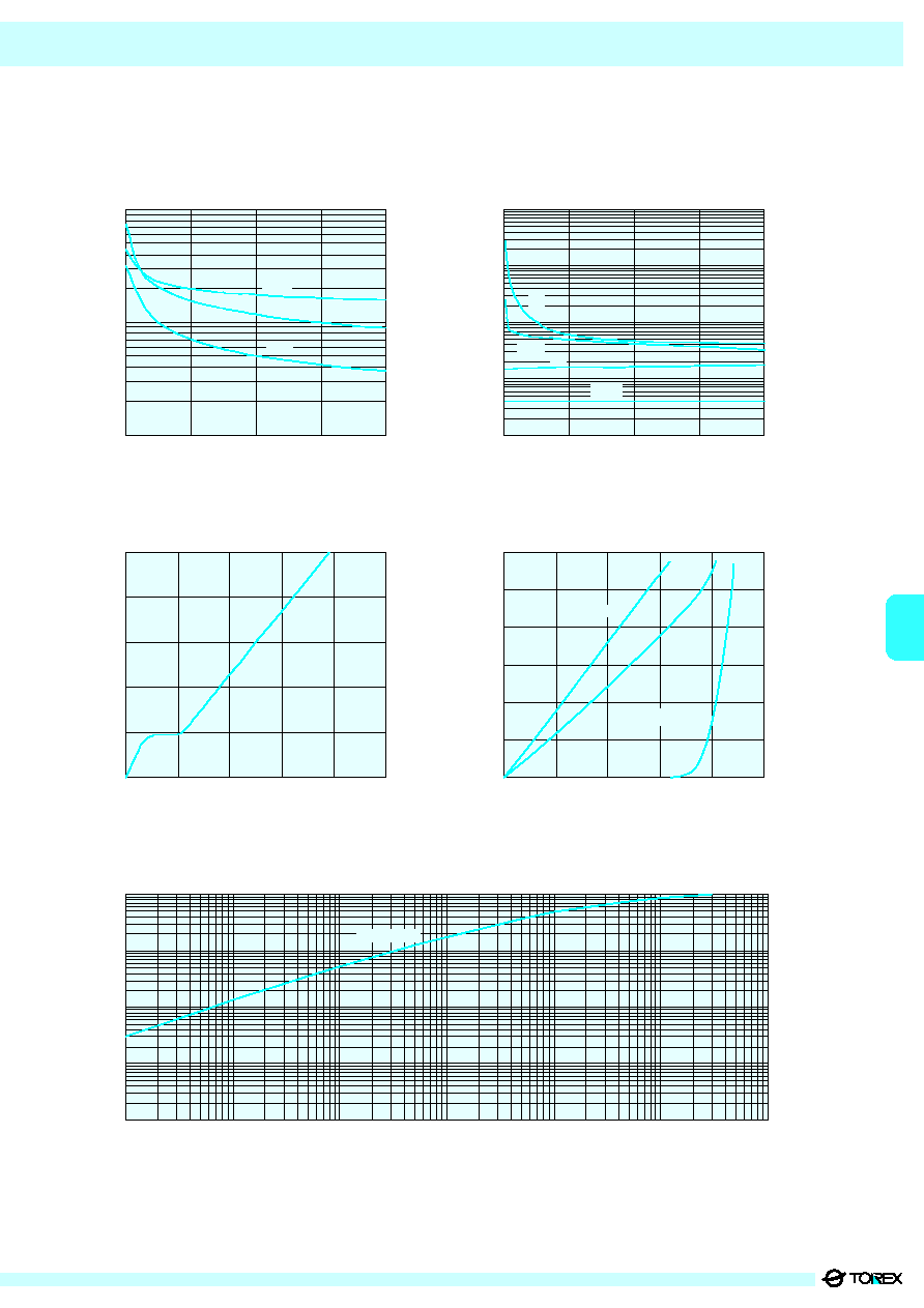
Electrical Characteristics
Drain/Source Voltage:Vds (V)
Drain Current:Id (A)
Switching Time:t (ns)
Vgs=-5V, Vdd-10V, PW=10s, duty1%, Ta=25
Switching Time vs. Drain Current
Capacitance vs. Drain/Source Voltage
-10
-8
-6
-4
-2
0
0
2
4
6
8
10
-3
-2.5
-2
-1.5
-1
-0.5
0
-1
-0.8
-0.6
-0.4
-0.2
0
Vgs=0V, 4.5V
-4.5V
-2.5V
0.0001
0.001
0.01
0.1
1
0.0001
0.001
0.01
0.1
1
10
100
Standardized Transition Thermal Resistance vs. Pulse Width
Pulse Width:PW (s)
Standardized Transition Thermal Resistance:s(t)
Single Pulse
Gate Charge:Qg (nc)
Source/Drain Voltage:Vsd (V)
Gate/Source Voltage:Vgs (V)
Reverse Drain Current:Idr (A)
Vds=-10V, Id=-0.7A, Ta=25
Gate/Source Voltage vs. Gate Charge
Reverse Drain Current vs. Source/Drain Voltage
Ta=25, Pulse Test
Rth(ch-a)=250/W (implemented on a ceramic PCB)