MIG300J2CSB1W
2001-11-13
1
TOSHIBA Intelligent Power Module Silicon N Channel IGBT
MIG300J2CSB1W
(600V/300A 2in1)
High Power
Switching
Applications
Motor Control Applications
∑ Integrates inverter power circuits and control circuits (IGBT drive unit, units for protection against short-circuit
current, overcurrent, undervoltage and overtemperature) into a single package.
∑ The electrodes are isolated from the case.
∑ Low thermal resistance
∑ V
CE (sat)
= 1.9 V (typ.)
∑ UL recognized: File No.E87989
∑ Weight: 278 g (typ.)
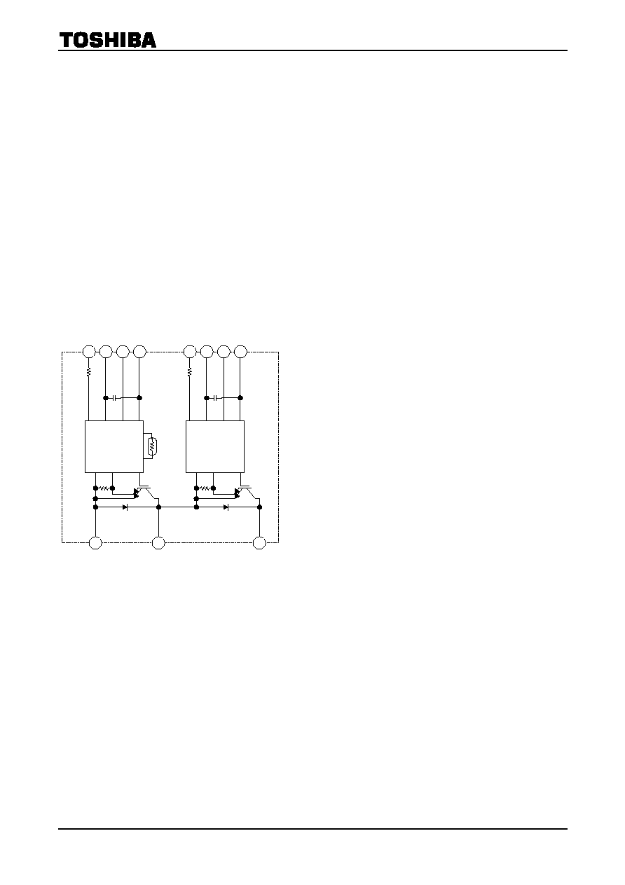
Equivalent Circuit
1. FO
(L) 2. GND
(L)
3. IN
(L)
4.
V
D
(L)
5. FO
(H) 6. GND
(H)
7. IN
(H) 8.
V
D
(H)
FO GND IN V
D
1
2
3
4
GND V
S
OUT
C2/E1
FO GND IN V
D
5
6
7
8
GND V
S
OUT
C1
E2
MIG300J2CSB1W
2001-11-13
2
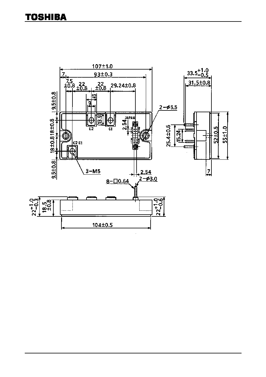
Package Dimensions: TOSHIBA 2-108H1A
Unit: mm
1. FO
(L) 2. GND
(L)
3. IN
(L)
4.
V
D
(L)
5. FO
(H) 6. GND
(H)
7. IN
(H) 8.
V
D
(H)
MIG300J2CSB1W
2001-11-13
3
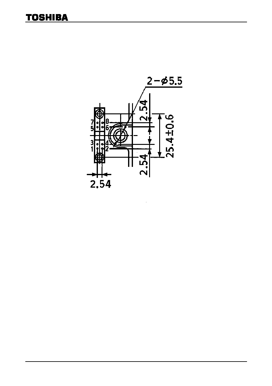
Signal Terminal Layout
Unit: mm
1. FO
(L) 2. GND
(L)
3. IN
(L)
4.
V
D
(L)
5. FO
(H) 6. GND
(H)
7. IN
(H) 8.
V
D
(H)

MIG300J2CSB1W
2001-11-13
4
Maximum Ratings
(T
j
=
=
=
=
25∞C)
Stage Characteristics
Condition
Symbol
Rating
Unit
Supply voltage
P-N power terminal
V
CC
450 V
Collector-emitter voltage
æ
V
CES
600 V
Collector current
Tc
=
25∞C, DC
I
C
300 A
Forward current
Tc
=
25∞C, DC
I
F
300
A
Collector power dissipation
Tc
=
25∞C
P
C
1600 W
Inverter
Junction temperature
æ
T
j
150
∞C
Control supply voltage
V
D
-GND terminal
V
D
20 V
Input voltage
IN-GND terminal
V
IN
20 V
Fault output voltage
FO-GND terminal
V
FO
20 V
Control
Fault output current
FO sink current
I
FO
10 mA
Operating temperature
æ
Tc
-
20~
+
100
∞C
Storage temperature
æ
T
stg
-
40~
+
125
∞C
Isolation voltage
AC 1 min
V
ISO
2500 V
Module
Screw torque
M5
æ
3
N
m
Electrical Characteristics
1. Inverter
stage
Characteristics Symbol
Test
Condition
Min
Typ.
Max
Unit
T
j
=
25∞C
æ
æ
1
Collector cut-off current
I
CEX
V
CE
=
600 V
T
j
=
125∞C
æ
æ
10
mA
T
j
=
25∞C
1.6 1.9 2.3
Collector-emitter saturation voltage
V
CE (sat)
V
D
=
15 V
I
C
=
300 A
V
IN
=
15 V
Æ
0 V
T
j
=
125∞C
æ
2.1
æ
V
Forward voltage
V
F
I
F
=
300 A, T
j
=
25∞C
æ
2.1 2.5
V
t
on
æ
2.0 3.0
t
c (on)
æ
0.4
æ
t
rr
æ
0.2
æ
t
off
æ
1.5 2.5
Switching time
t
c (off)
V
CC
=
300 V, I
C
=
300 A
V
D
=
15 V, V
IN
=
15 V
´
0 V
T
j
=
25∞C, Inductive load
(Note 1)
æ
0.25
æ
m
s
Note 1: Switching time test circuit & timing chart

MIG300J2CSB1W
2001-11-13
5
2. Control
stage
(T
j
=
=
=
=
25∞C)
Characteristics Symbol
Test
Condition
Min
Typ.
Max
Unit
High side
I
D (H)
æ
13 17
Control circuit current
Low side
I
D (L)
V
D
=
15 V
æ
13 17
mA
Input on signal voltage
V
IN (on)
1.4 1.6 1.8
Input off signal voltage
V
IN (off)
V
D
=
15 V
2.2 2.5 2.8
V
Protection I
FO (on)
æ
10 12
Fault output current
Normal I
FO (off)
V
D
=
15 V
æ
æ
0.1
mA
Overcurrent protection trip
level
Inverter OC
V
D
=
15 V, T
j
<
=
125∞C 480
æ
æ
A
Short-circuit protection
trip level
Inverter SC
V
D
=
15 V, T
j
<
=
125∞C 480
æ
æ
A
Overcurrent cut-off time
t
off (OC)
V
D
=
15 V
æ
5
æ
m
s
Trip
level
OT
110 118 125
Overtemperature
protection
Reset level
OTr
Case temperature
æ
98
æ
∞C
Trip
level
UV
11.5 12.0 12.5
Control supply under
voltage protection
Reset level
UVr
æ
12.0 12.5 13.0
V
Fault output pulse width
t
FO
V
D
=
15
V
1 2 3 ms
3. Thermal
resistance
(Tc
=
=
=
=
25∞C)
Characteristics Symbol
Test
Condition
Min
Typ.
Max
Unit
IGBT
æ
æ
0.078
Junction to case thermal resistance
R
th (j-c)
FRD
æ
æ
0.130
∞C/W
Case to fin thermal resistance
R
th (c-f)
Compound
is
applied
æ
0.017
æ
∞C/W