SM12G45,SM12J45,SM12G45A,SM12J45A
2001-07-13
1
TOSHIBA
BI-DIRECTIONAL TRIODE THYRISTOR SILICON PLANAR TYPE
SM12G45,SM12J45,SM12G45A,SM12J45A
AC POWER CONTROL APPLICATIONS
l Repetitive Peak Off-State Voltage : V
DRM
= 400, 600V
l R.M.S On-State Current
: I
T (RMS)
= 12A
l High Commutating (dv / dt)
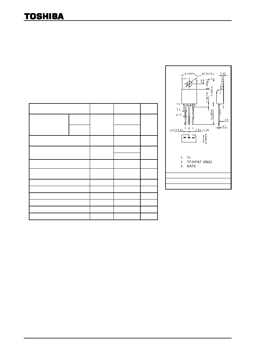
MAXIMUM RATINGS
Unit: mm
JEDEC TO-220AB
JEITA
TOSHIBA 13-10G1A
Weight: 2.0g
CHARACTERISTIC SYMBOL
RATING
UNIT
SM12G45
SM12G45A
400
Repetitive Peak
Off
-State Voltage
SM12J45
SM12J45A
V
DRM
600
V
R.M.S On
-State Current
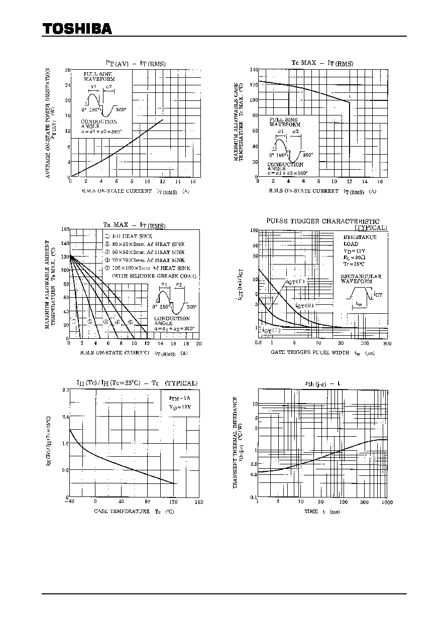
(Full Sine Waveform Tc = 98∞C)
I
T (RMS)
12 A
120 (50Hz)
Peak One Cycle Surge On
-State
Current (Non
-Repetitive)
I
TSM
132 (60Hz)
A
I
2
t Limit Value (t = 1~10ms)
I
2
t 72
A
2
s
Critical Rate of Rise of On-State
Current
di / dt
50
A / µs
Peak Gate Power Dissipation
P
GM
5 W
Average Gate Power Dissipation
P
G (AV)
0.5 W
Peak Gate Voltage
V
GM
10 V
Peak Gate Current
I
GM
2 A
Junction Temperature
T
j
-40~125 ∞C
Storage Temperature Range
T
stg
-40~125 ∞C
SM12G45,SM12J45,SM12G45A,SM12J45A
2001-07-13
2
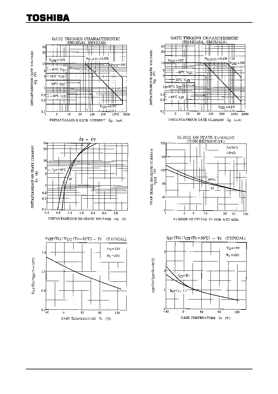
ELECTRICAL CHARACTERISTICS
(Ta = 25∞C)
CHARACTERISTIC SYMBOL
TEST
CONDITION
MIN
TYP.
MAX
UNIT
Repetitive Peak Off-State Current
I
DRM
V
DRM
=Rated, T
j
= 125∞C
2 mA
I
T2 (+) , Gate (+)
2
II
T2 (+) , Gate (-)
2
III T2
(-) , Gate (-)
2
SM12G45
SM12J45
IV T2
(-) , Gate (+)
I
T2 (+) , Gate (+)
1.5
II
T2 (+) , Gate (-)
1.5
III T2
(-) , Gate (-)
1.5
Gate Trigger
Voltage
SM12G45A
SM12J45A
IV
V
GT
V
D
= 12V,
R
L
= 20
T2 (-) , Gate (+)
V
I
T2 (+) , Gate (+)
30
II
T2 (+) , Gate (-)
30
III T2
(-) , Gate (-)
30
SM12G45
SM12J45
IV T2
(-) , Gate (+)
I
T2 (+) , Gate (+)
20
II
T2 (+) , Gate (-)
20
III T2
(-) , Gate (-)
20
Gate Trigger
Current
SM12G45A
SM12J45A
IV
I
GT
V
D
= 12V,
R
L
= 20
T2 (-) , Gate (+)
mA
Peak On-State Voltage
V
TM
I
TM
= 17A
1.5 V
Gate Non-Trigger Voltage
V
GD
V
D
= Rated, Tc = 125∞C
0.2
V
Holding Current
I
H
V
D
= 12V, I
TM
= 1A
50 mA
Thermal Resistance
R
th (j-c)
Junction to Case, AC
1.8
∞C
/
W
SM12G45
SM12J45
10
Critical Rate of Rise of
Off-State Voltage at
Commutation
SM12G45A
SM12J45A
(dv / dt) c
V
DRM
= 400V
(di / dt) c = - 6.5A / ms
4
V / µs
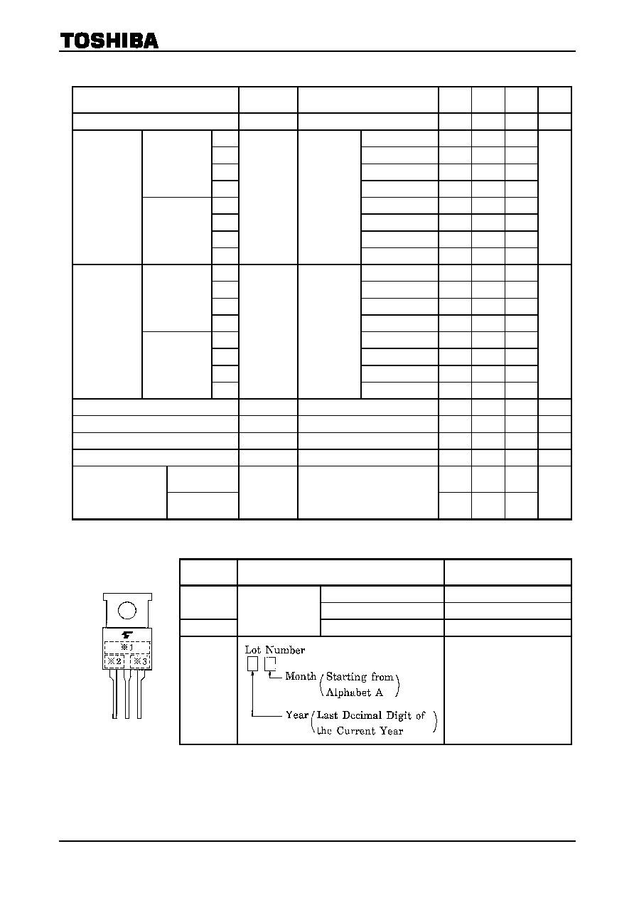
MARKING
NUMBER SYMBOL
MARK
SM12G45, SM12G45A
M12G45
*1
SM12J45, SM12J45A
M12J45
*2
TYPE
SM12G45A, SM12J45A
A
*3
Example
8A : January 1998
8B : February 1998
8L : December 1998
SM12G45,SM12J45,SM12G45A,SM12J45A
2001-07-13
5
∑ TOSHIBA is continually working to improve the quality and reliability of its products. Nevertheless, semiconductor
devices in general can malfunction or fail due to their inherent electrical sensitivity and vulnerability to physical
stress. It is the responsibility of the buyer, when utilizing TOSHIBA products, to comply with the standards of
safety in making a safe design for the entire system, and to avoid situations in which a malfunction or failure of
such TOSHIBA products could cause loss of human life, bodily injury or damage to property.
In developing your designs, please ensure that TOSHIBA products are used within specified operating ranges as
set forth in the most recent TOSHIBA products specifications. Also, please keep in mind the precautions and
conditions set forth in the "Handling Guide for Semiconductor Devices," or "TOSHIBA Semiconductor Reliability
Handbook" etc..
∑ The TOSHIBA products listed in this document are intended for usage in general electronics applications
(computer, personal equipment, office equipment, measuring equipment, industrial robotics, domestic appliances,
etc.). These TOSHIBA products are neither intended nor warranted for usage in equipment that requires
extraordinarily high quality and/or reliability or a malfunction or failure of which may cause loss of human life or
bodily injury ("Unintended Usage"). Unintended Usage include atomic energy control instruments, airplane or
spaceship instruments, transportation instruments, traffic signal instruments, combustion control instruments,
medical instruments, all types of safety devices, etc.. Unintended Usage of TOSHIBA products listed in this
document shall be made at the customer's own risk.
∑ The information contained herein is presented only as a guide for the applications of our products. No
responsibility is assumed by TOSHIBA CORPORATION for any infringements of intellectual property or other
rights of the third parties which may result from its use. No license is granted by implication or otherwise under
any intellectual property or other rights of TOSHIBA CORPORATION or others.
∑ The information contained herein is subject to change without notice.
000707EAA
RESTRICTIONS ON PRODUCT USE