 | –≠–ª–µ–∫—Ç—Ä–æ–Ω–Ω—ã–π –∫–æ–º–ø–æ–Ω–µ–Ω—Ç: T6B70BF | –°–∫–∞—á–∞—Ç—å:  PDF PDF  ZIP ZIP |

T6B70BF
2003-03-13
1
TOSHIBA CMOS Digital Integrated Circuit Silicon Monolithic
T6B70BF
Interface IC for Water Heater
The T6B70BF incorporates two-channel 4-bit DA converter, a
pseudo sine wave generator and an external analog signal
detection/non-detection circuit. It is designed to be used mainly
for communication between water heater and control unit.
Features
∑ On-chip two-channel 4-bit DA converter (opposite polarities)
∑ On-chip pseudo sine wave generator (external clock/16)
∑ On-chip external analog signal detection/non-detection circuit
∑ On-chip two-channel analog switch
Block Diagram
Weight: 0.16 g (typ.)
Divide-by-
16 unit
Pseudo
sine wave
generator
Waveform
initialization block
Modulation
control circuit
Reset
circuit
Zero-cross
waveform
shaping circuit
Cycle measurement counter
Analog signal
detection/non-detection
Amplifier input
circuit
4-bit
DA converter
4-bit
DA converter
1
2
3
4
14
15
11
10
5
13
12
16
7
6
8
9
OSCIN
OSCOUT
FOUT
SCTL
SW1IN
SW1OUT
SW2IN
SW2OUT
RESET
SOUT+
SOUT-
V
DD
AMPIN
AMPOUT
V
SS
DOUT
0∞C
180∞C
Output buffer
T6B70BF
2003-03-13
2
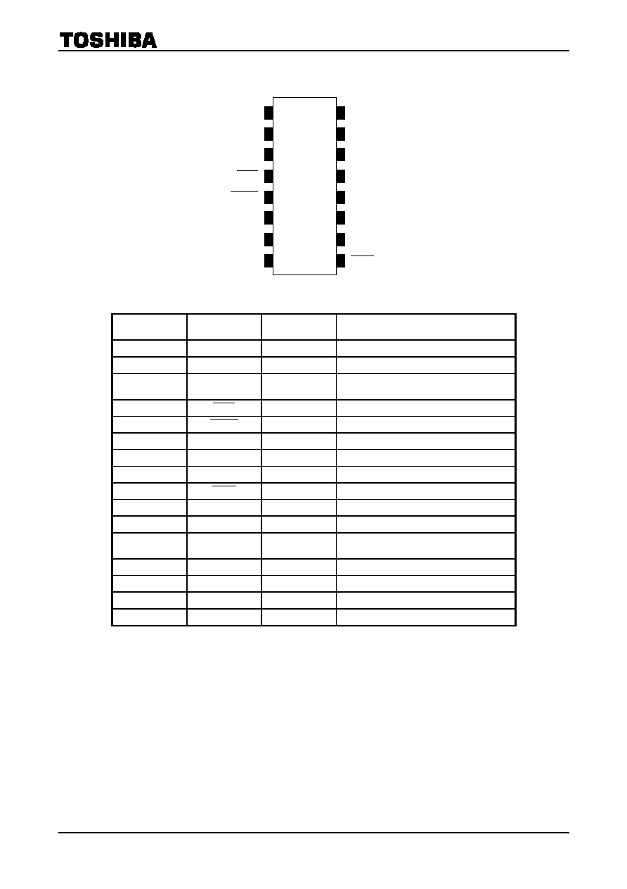
Pin Assignment
Pin Function
No. Symbol
Input/Output
Function
1
OSCIN
Input
Pins connected to oscillation
2
OSCOUT
Output
Pins connected to oscillation
3 FOUT
Output
Output pin for oscillation waveform shaping
circuit
4
SCTL
Input
Modulation control signal input pin
5
RESET
Input
Reset
signal
input
pin
6
AMPOUT
Output
Amplifier signal output pin
7 AMPIN
Input
Amplifier
signal
input
pin
8 V
SS
Device GND pin (0 V)
9
DOUT
Output
Output pin for amplifier input signal detector
10
SW2OUT
Output
Output pin on analog SW2 side
11
SW2IN
Input
Input pin on analog SW2 side
12 SOUT- Output
Pseudo sine wave (opposite polarity of
SOUT+ output) output pin
13
SOUT+
Output
Pseudo sine wave output pin
14
SW1IN
Input
Input pin on analog SW1 side
15
SW1OUT
Output
Output pin on analog SW1 side
16 V
DD
Device power supply pin (+5 V)
OSCIN
SOUT+
SOUT-
V
DD
AMPIN
AMPOUT
V
SS
DOUT
OSCOUT
FOUT
SCTL
SW1IN
SW1OUT
SW2IN
SW2OUT
RESET
1
2
3
4
5
6
7
8
16
15
14
13
12
11
10
9
T6B70BF

T6B70BF
2003-03-13
3
Function Description
(1) Pseudo sine wave generator and 4-bit DA converters (sending block)
Pseudo sine wave signal with Fosc/16 frequency is driven out from pseudo sine wave output pin
(SOUT+ and SOUT-).
The outputs of pins SOUT+ and SOUT- have the opposite polarities.
The block of pseudo sine wave generator and 4-bit DA converter (the side of SOUT+ pin) are shown
below.
The data of pseudo sine wave generator is driven out in the following sequence.
0 1 3 6 9 C E F F E C 9 6 3 1 0 (in hexadecimal)
Thus, the pseudo sine waveform of positive-going and negative-going outputs is like a staircase at
no load.
An analog switch is incorporated so that the driver output buffer is connected to the transmission
line only when transmission is performed.
However, an emitter follower circuit is externally connected to the driver output buffer.
The phase difference between positive-going and negative-going outputs is within 180∞ ± 5∞. (pseudo
sine wave output phase fluctuation)
P
s
eudo s
i
ne
wav
e
generat
or
FOSC
RST
MSB
R
V
SS
R
R R
R R
R
R
LSB
R
R
R
2R
SOUT+ pin
SOUT+
SOUT-
F
250 kHz
F
E
C
9
6
3
1
0
E
C
9
6
3
1 0
FSIN
@FOSC = 4 MHz

T6B70BF
2003-03-13
4
(2) Amplifier input circuit and signal detection/non-detection circuit (receiving block)
The modulation signal input block incorporates two level comparators having a high and a low
threshold values to detect the external sine wave signal with amplitude higher than the specified
threshold. Thus, it avoids signals with amplitude lower than the specified threshold (e.g., noise
signals) being detected erroneously.
The detection frequency range (frequency window) is determined by the divider ratio 1/18 to 1/14 of
Fosc.
In detection/non-detection determined condition, when the signals within the specified frequency
range are detected (or not detected) sequentially, signals are controlled using the majority rule. The
time which detection/non-detection is determined takes 9 to 15 waves to pass when one wave is
referenced to Fosc/16 frequency.
VH
VL
Input
sensitivity
V
PP
Detect reception
Not detect reception
Not detect reception
Not detect reception
AMPIN input sine waveform
AMPOUT output timing (when
RESET
is Low)
VH
VL
Held at High
Held at Low
VBIAS
VBIAS < VL
VBIAS > VH
VH > VBIAS > VL VH > VBIAS > VL
AMPOUT
AMPOUT Truth Table
VA
VB
AMPOUT
VBIAS > VH
L
H
L
VH > VBIAS > VL
H
H
Hold
VBIAS < VL
H
L
H
R1
R2
R3
R4
V
SS
V
SS
APU
APD
7
V
DD
V
DD
AMPIN pin
Reference
voltage
VH
Reference
voltage
VL
High comparator
VA
6
AMPOUT pin
9
DOUT
pin
Cycle
measurement
counter
Analog
signal
detection
/non-
detection
circuit
Low comparator
VB
RESET
V
DD
R
Q
S
Q
RESET
VBIAS

T6B70BF
2003-03-13
5
(3) Function description and timing chart of the sending block
When modulation control input ( SCTL ) is in High-level, pseudo sine wave output is held at 0∞ of
the phase angle of pseudo sine wave. When modulation control input changes from High-level to
Low-level, the pseudo sine wave output (SOUT+) starts from -90∞ (SOUT- starts from +90∞).
In this case, the time which takes to turn ON is as follows.
td (ON) < 500 ns
When modulation control input changes from Low-level to High-level, the phase angle is forcibly
held at 0∞, regardless of the phase of the pseudo sine wave output. (the pseudo sine wave output is
stopped). In this case, the time which takes to turn OFF is as follows.
td (OFF) < 1 µs
(4) Function description and timing chart of the receiving block
When it is ready to receive amplifier input signal, the time T (DET) which takes to change from
High to Low at DOUT pin is within the time which 9 to 15 waves to pass. In this case, one wave is
referenced to 16 Fosc clocks. The time width is determined by the internal clock and amplifier input
signal. The timings of the internal clock and internal detection signal in the majority logic circuit are
synchronous with each other. When input signals with the cycle, which is within the range specified
by the frequency window, are detected (or not detected) sequentially, this rule is valid (the majority
rule).
Note 1: Any communication protocol is used, however, it takes 15 carrier waves to pass when the signal changes its
state.
DOUT
T (DET)
T (DET)
Amplifier input
td (ON)
SCTL
SOUT+ pseudo sine wave output
(SOUT- output pin has the
opposite polarity)
td (OFF)

T6B70BF
2003-03-13
6
Timing Chart
(SOUT+ = SW1IN, SW1OUT, SOUT- = SW2IN, SW2OUT)
TDET
When receiving
TDET
V
OPP
FSIN
When sending
td (ON)
td (OFF)
High-z
V
PP
V
DD
RESET
OSCIN
(4 MHz)
FOUT
AMPOUT
AMPIN
(250 kHz)
SCTL
SOUT+
SOUT-
DOUT
SW1IN
SW1OUT
SW2IN
SW2OUT
High-z
High-z
High-z
High-z
T6B70BF
2003-03-13
7
Maximum Ratings
(Ta = 25∞C ± 1.5∞C)
Characteristics Symbol
Rating
Unit
Power supply voltage
V
DD
-0.3 to 6.0
V
Input voltage
VI
-0.3 to V
DD
+ 0.3
V
Input peak current
IIK
-20 to 20
mA
Operating temperature
T
opr
-20 to 80
∞C
Storage temperature
T
stg
-55 to 125
∞C
Power dissipation
P
D
(Note 1)
0.54 W
Note 1: Decreases approximately 4.35 mW per 1∞C.
Electrical Characteristics
(unless otherwise specified, V
DD
= 5.0 V, V
SS
= 0 V, FOSC = 4 MHz and Ta = -20 to 80∞C)
Characteristics Symbol
Test
Circuit
Test Condition
Min
Typ.
Max
Unit
V
DD
pin (pin 16)
Operating voltage
V
DD
4.5 5.0 5.5 V
Current consumption
I
DD
1
No load, Fosc = 4 MHz
10 mA
OSCIN pin (pin 1) and OSCOUT pin (pin 2)
Oscillation frequency
FOSC
2
1
4
10
MHz
High level
VIHOSC
3
0.7
V
DD
V
DD
Input voltage
Low level
VILOSC
3
V
SS
0.3
V
DD
V
High level
IIHROSC
4
VIN = 5 V, Ta = 25∞C
3.2
6.58
13.2
Input current
Low level
IILROSC
4
VIN = 0 V, Ta = 25∞C
-3.2
-6.58 -13.2
µA
High level
VOHOSC
3
IOH = -0.1 mA
V
DD
-
1.0
V
DD
Output voltage
Low level
VOLOSC
4
IOL = +0.1 mA
V
SS
V
SS
+
0.6
V
RESET
pin (pin 5)
Low to High input switching level
VIHRST
5
0.65
V
DD
V
DD
V
High to Low input switching level
VILRST
5
V
SS
0.35
V
DD
V
High-level input current
IIHRST
6
VIN = V
DD
-10
10 µA
Pull-up resistance 1
IILRRST1
7
VIN = V
SS
, Ta = 25
9
15
21
k
Pull-up resistance 2
IILRRST2
7
VIN = V
SS
, Ta = -20 to 80
6.3
27.3
k
SCTL
pin (pin 4)
Low to High input switching level
VIHSCTL
8
0.65
V
DD
V
DD
V
High to Low input switching level
VILSCTL
8
V
SS
0.35
V
DD
V
High level
IIHSCTL
9
VIN = V
DD
-1
1
Input current
Low level
IILSCTL
9
VIN = V
DD
-1
1
µA
FOUT pin (pin 3)
High level
VOHFOUT
10
IOH = -1.0 mA
V
DD
-
1.0
V
DD
Output voltage
Low level
VOLFOUT
11
IOL = +1.0 mA
V
SS
V
SS
+
0.6
V
Note 2: One direction in which current flow into the IC should be + (sink) and the other direction in which current
flow out from the IC should be - (drain).

T6B70BF
2003-03-13
8
Characteristics Symbol
Test
Circuit
Test Condition
Min
Typ.
Max
Unit
DOUT
pin (pin 9)
High level
VOHDOUT
12
IOH = -1.0 mA
V
DD
-
1.0
V
DD
Output voltage
Low level
VOLDOUT
13
IOL = +1.0 mA
V
SS
V
SS
+
0.6
V
Non-reception to reception detection
time
TDET1 19
Fosc = 4 MHz,
AMPIN = 250 kHz
Time which takes
DOUT
to
change from High to Low
40
60 µs
Reception to non-reception detection
time
TDET2 19
Fosc = 4 MHz,
AMPIN = 250 kHz
Time which takes
DOUT
to
change from Low to High
36
56 µs
AMPIN pin (pin 7)
Input dynamic range
VAMPIN
14
V
SS
V
DD
V
Pull-up resistance 1
IILRAPU1
15
VIN = V
SS
, Ta = 25
11.6
19.4
27.2
k
Pull-up resistance 2
IILRAPU2
15
VIN = V
SS
, Ta = -20 to 80
7
38 k
Pull-down resistance 1
IIHRAPD1
16
VIN = V
DD
, Ta = 25
5.9
9.8
13.7
k
Pull-down resistance 2
IIHRAPD2
16
VIN = V
DD
, Ta = -20 to 80
3
19.2
k
Amplifier input bias voltage
VBIAS
17
No load (design goal)
1.54
1.63
1.71
V
Amplifier input sensitivity
V
PP
18
No load, receivable amplitude
range is 250 kHz, when sine
wave signal is applied.
(design goal)
0.3
0.45
V
Detection frequency range
DETON
19
Fosc = 4 MHz
236
266
kHz
Non-detection frequency
(low frequency)
DETOFF1
19
Fosc = 4 MHz
222
kHz
Non-detection frequency
(high frequency)
DETOFF2
19
Fosc = 4 MHz
286
kHz
SW1IN pin (pin 14) and SW1OUT pin (pin 15)
Analog switch input voltage
VINASW1
V
SS
V
DD
V
Analog switch output voltage
VOUTASW1
V
SS
V
DD
V
OFF-leak current of analog switch 1
IOFFASW1
20
SCTL
= H, SW1IN = V
DD
,
SW1OUT = V
SS
-1
1 µA
ON-resistance of analog switch 1
RONASW1
21
SCTL
= L, SW1IN = 5 V,
SW1OUT = 0 V
Current measure
35
105
SW2IN pin (pin 11) and SW2OUT pin (pin 10)
Analog switch input voltage
VINASW2
V
SS
V
DD
V
Analog switch output voltage
VOUTASW2
V
SS
V
DD
V
OFF-leak current of analog switch 2
IOFFASW2
20
SCTL
= H, SW2IN = V
DD
,
SW2OUT = V
SS
-1
1 µA
ON-resistance of analog switch 2
RONASW2
21
SCTL
= L, SW2IN = 5 V,
SW2OUT = 0 V
Current measure
35
105
SOUT+ pin (pin 13) and SOUT- pin (pin 12)
Output voltage
V
OPP
22
Maximum voltage value at no
load
0.85
V
DD
V
DD
V
Pseudo sine wave output frequency
FSIN
23
FOSC = 4 MHz
250 kHz
Pseudo sine wave output start time
tdON
23
SCTL
= H L
500
ns
Pseudo sine wave output stop time
tdOFF
23
SCTL
= L H
1 µs
Equivalent output impedance
ROUTSIN
24
No load
2.8
4
5.2
k
Note:
One direction in which current flow into the IC should be + (sink) and the other direction in which current
flow out from the IC should be - (drain).

T6B70BF
2003-03-13
9
Test Circuit
(1) Current
consumption
(2) Oscillation
frequency
(3) High-level
input
voltage
Low-level input voltage
High-level output voltage
(4) High-level
input
current
Low-level input current
Low-level output voltage
(5) Low to High input switching level
High to Low input switching level
(6) High-level
input
current
2
3
6
7
4 MHz
PG
13
12
9
OSCIN
OSCOUT
FOUT
SCTL
SW1IN
SW1OUT
SW2IN
SW2OUT
RESET
SOUT+
SOUT-
V
DD
AMPIN
AMPOUT
V
SS
DOUT
15
14
10
11
A
16
1
4
5
8
ICC
5 V
2
3
6
7
VOHOSC
13
12
9
OSCIN
OSCOUT
FOUT
SCTL
SW1IN
SW1OUT
SW2IN
SW2OUT
RESET
SOUT+
SOUT-
V
DD
AMPIN
AMPOUT
V
SS
DOUT
15
14
10
11
16
1
4
5
8
5 V
V
IO
H
-
0.
1 m
A
VILOSC
VIHOSC
13
12
9
OSCIN
OSCOUT
FOUT
SCTL
SW1IN
SW1OUT
SW2IN
SW2OUT
RESET
SOUT+
SOUT-
V
DD
AMPIN
AMPOUT
V
SS
DOUT
15
14
10
11
16
5 V
IILROSC
IIHROSC
VOLOUT V
IO
L
+0.
1
m
A
A
VIN
2
3
6
7
1
4
5
8
A
VIN
2
3
6
7
13
12
9
OSCIN
OSCOUT
FOUT
SCTL
SW1IN
SW1OUT
SW2IN
SW2OUT
RESET
SOUT+
SOUT-
V
DD
AMPIN
AMPOUT
V
SS
DOUT
15
14
10
11
16
1
4
5
8
5 V
IIHRST
Monitor
Fosc
2
3
6
7
1 to 10 MHz
PG
13
12
9
OSCIN
OSCOUT
FOUT
SCTL
SW1IN
SW1OUT
SW2IN
SW2OUT
RESET
SOUT+
SOUT-
V
DD
AMPIN
AMPOUT
V
SS
DOUT
15
14
10
11
16
1
4
5
8
5 V
2
3
6
7
4 MHz
PG
13
12
9
OSCIN
OSCOUT
FOUT
SCTL
SW1IN
SW1OUT
SW2IN
SW2OUT
RESET
SOUT+
SOUT-
V
DD
AMPIN
AMPOUT
V
SS
DOUT
15
14
10
11
16
1
4
5
8
5 V
VILRST
VIHRST
Monitor
Monitor

T6B70BF
2003-03-13
10
(7) Pull-up resistance 1
Pull-up resistance 2
(8) Low to High input switching level
High to Low input switching level
(9) High-level
input
current
Low-level input current
(10) High-level output voltage
(11) Low-level output voltage
(12) High-level output voltage
A
2
3
6
7
13
12
9
OSCIN
OSCOUT
FOUT
SCTL
SW1IN
SW1OUT
SW2IN
SW2OUT
RESET
SOUT+
SOUT-
V
DD
AMPIN
AMPOUT
V
SS
DOUT
15
14
10
11
16
1
4
5
8
5 V
IILRRST2
IILRRST1
A
VIN
2
3
6
7
13
12
9
OSCIN
OSCOUT
FOUT
SCTL
SW1IN
SW1OUT
SW2IN
SW2OUT
RESET
SOUT+
SOUT-
V
DD
AMPIN
AMPOUT
V
SS
DOUT
15
14
10
11
16
1
4
5
8
5 V
IILSCTL
IIHSCTL
13
12
9
OSCIN
OSCOUT
FOUT
SCTL
SW1IN
SW1OUT
SW2IN
SW2OUT
RESET
SOUT+
SOUT-
V
DD
AMPIN
AMPOUT
V
SS
DOUT
15
14
10
11
16
5 V
VOLFOUT V
IO
L
+1.
0
m
A
2
3
6
7
1
4
5
8
2
3
6
7
VOHFOUT
13
12
9
OSCIN
OSCOUT
FOUT
SCTL
SW1IN
SW1OUT
SW2IN
SW2OUT
RESET
SOUT+
SOUT-
V
DD
AMPIN
AMPOUT
V
SS
DOUT
15
14
10
11
16
1
4
5
8
5 V
V
IO
H
-
1.
0 m
A
2
3
6
7
4 MHz
PG
13
12
9
OSCIN
OSCOUT
FOUT
SCTL
SW1IN
SW1OUT
SW2IN
SW2OUT
RESET
SOUT+
SOUT-
V
DD
AMPIN
AMPOUT
V
SS
DOUT
15
14
10
11
16
1
4
5
8
5 V
VOHDOUT V
IO
H
-
1.
0 m
A
2
3
6
7
4 MHz
PG
13
12
9
OSCIN
OSCOUT
FOUT
SCTL
SW1IN
SW1OUT
SW2IN
SW2OUT
RESET
SOUT+
SOUT-
V
DD
AMPIN
AMPOUT
V
SS
DOUT
15
14
10
11
16
1
4
5
8
5 V
VILSCTL
VIHSCTL
Monitor
Monitor

T6B70BF
2003-03-13
11
(13) Low-level output voltage
(14) Input dynamic range
(15) Pull-up resistance 1
Pull-up resistance 2
(16) Pull-down resistance 1
Pull-down resistance 2
(17) Amplifier input bias voltage
(18) Amplifier input sensitivity
A
2
3
6
7
13
12
9
OSCIN
OSCOUT
FOUT
SCTL
SW1IN
SW1OUT
SW2IN
SW2OUT
RESET
SOUT+
SOUT-
V
DD
AMPIN
AMPOUT
V
SS
DOUT
15
14
10
11
16
1
4
5
8
5 V
IILRAPU2
IILRAPU1
2
3
6
7
13
12
9
OSCIN
OSCOUT
FOUT
SCTL
SW1IN
SW1OUT
SW2IN
SW2OUT
RESET
SOUT+
SOUT-
V
DD
AMPIN
AMPOUT
V
SS
DOUT
15
14
10
11
16
1
4
5
8
5 V
V
VBIAS
2
3
6
7
13
12
9
OSCIN
OSCOUT
FOUT
SCTL
SW1IN
SW1OUT
SW2IN
SW2OUT
RESET
SOUT+
SOUT-
V
DD
AMPIN
AMPOUT
V
SS
DOUT
15
14
10
11
16
1
4
5
8
5 V
A
VIN
IIHRAPD2
IIHRAPD1
2
3
6
7
4 MHz
PG
13
12
9
OSCIN
OSCOUT
FOUT
SCTL
SW1IN
SW1OUT
SW2IN
SW2OUT
RESET
SOUT+
SOUT-
V
DD
AMPIN
AMPOUT
V
SS
DOUT
15
14
10
11
16
1
4
5
8
5 V
VOLDOUT V
IO
L
+1.
0
m
A
VAMPIN
2
3
6
7
4 MHz
PG
13
12
9
OSCIN
OSCOUT
FOUT
SCTL
SW1IN
SW1OUT
SW2IN
SW2OUT
RESET
SOUT+
SOUT-
V
DD
AMPIN
AMPOUT
V
SS
DOUT
15
14
10
11
16
1
4
5
8
5 V
Monitor
V
p-p
2
3
6
7
4 MHz
PG
13
12
9
OSCIN
OSCOUT
FOUT
SCTL
SW1IN
SW1OUT
SW2IN
SW2OUT
RESET
SOUT+
SOUT-
V
DD
AMPIN
AMPOUT
V
SS
DOUT
15
14
10
11
16
1
4
5
8
5 V
Monitor
250 kHz
sine wave

T6B70BF
2003-03-13
12
(19) Detection frequency range
Non-detection frequency (low frequency)
Non-detection frequency (high frequency)
Non-reception to reception detection time
Reception to non-reception detection time
(20) OFF-leak current of analog switch 1
OFF-leak current of analog switch 2
(21) ON-resistance of analog switch 1
ON-resistance of analog switch 2
(22) Output voltage
(23) Pseudo sine wave output frequency
Pseudo sine wave output start time
Pseudo sine wave output stop time
(24) Equivalent output impedance
2
3
6
7
13
12
9
OSCIN
OSCOUT
FOUT
SCTL
SW1IN
SW1OUT
SW2IN
SW2OUT
RESET
SOUT+
SOUT-
V
DD
AMPIN
AMPOUT
V
SS
DOUT
15
14
10
11
16
1
4
5
8
5.
0 V
5 V
A
RONASW1
A
RONASW2
5.
0 V
5.
0 V
2
3
6
7
13
12
9
OSCIN
OSCOUT
FOUT
SCTL
SW1IN
SW1OUT
SW2IN
SW2OUT
RESET
SOUT+
SOUT-
V
DD
AMPIN
AMPOUT
V
SS
DOUT
15
14
10
11
16
1
4
5
8
5 V
A
IOFFASW1
A
IOFFASW2
5.
0 V
2
3
6
7
4 MHz
PG
13
12
9
OSCIN
OSCOUT
FOUT
SCTL
SW1IN
SW1OUT
SW2IN
SW2OUT
RESET
SOUT+
SOUT-
V
DD
AMPIN
AMPOUT
V
SS
DOUT
15
14
10
11
16
1
4
5
8
5 V
V
OPP
V
V
V
OPP
2
3
6
7
4 MHz
PG
13
12
9
OSCIN
OSCOUT
FOUT
SCTL
SW1IN
SW1OUT
SW2IN
SW2OUT
RESET
SOUT+
SOUT-
V
DD
AMPIN
AMPOUT
V
SS
DOUT
15
14
10
11
16
1
4
5
8
5 V
5.
0 V
A
ROUTSIN
A
5.
0 V
ROUTSIN
2
3
6
7
4 MHz
PG
13
12
9
OSCIN
OSCOUT
FOUT
SCTL
SW1IN
SW1OUT
SW2IN
SW2OUT
RESET
SOUT+
SOUT-
V
DD
AMPIN
AMPOUT
V
SS
DOUT
15
14
10
11
16
1
4
5
8
5 V
Monitor DEGSOUT
FSIN
Monitor
tdOFF
tdON
2
3
6
7
4 MHz
PG
13
12
9
OSCIN
OSCOUT
FOUT
SCTL
SW1IN
SW1OUT
SW2IN
SW2OUT
RESET
SOUT+
SOUT-
V
DD
AMPIN
AMPOUT
V
SS
DOUT
15
14
10
11
16
1
4
5
8
5 V
DETOFF2
DETOFF1
Monitor
200 to 300 kHz
PG
DETON
TDET2
TDET1

T6B70BF
2003-03-13
13
Markings
LOT CODE
T6B70BF

T6B70BF
2003-03-13
14
Package Dimensions
Weight: 0.16 g (typ.)

T6B70BF
2003-03-13
15
∑ TOSHIBA is continually working to improve the quality and reliability of its products. Nevertheless, semiconductor
devices in general can malfunction or fail due to their inherent electrical sensitivity and vulnerability to physical
stress. It is the responsibility of the buyer, when utilizing TOSHIBA products, to comply with the standards of
safety in making a safe design for the entire system, and to avoid situations in which a malfunction or failure of
such TOSHIBA products could cause loss of human life, bodily injury or damage to property.
In developing your designs, please ensure that TOSHIBA products are used within specified operating ranges as
set forth in the most recent TOSHIBA products specifications. Also, please keep in mind the precautions and
conditions set forth in the "Handling Guide for Semiconductor Devices," or "TOSHIBA Semiconductor Reliability
Handbook" etc..
∑ The TOSHIBA products listed in this document are intended for usage in general electronics applications
(computer, personal equipment, office equipment, measuring equipment, industrial robotics, domestic appliances,
etc.). These TOSHIBA products are neither intended nor warranted for usage in equipment that requires
extraordinarily high quality and/or reliability or a malfunction or failure of which may cause loss of human life or
bodily injury ("Unintended Usage"). Unintended Usage include atomic energy control instruments, airplane or
spaceship instruments, transportation instruments, traffic signal instruments, combustion control instruments,
medical instruments, all types of safety devices, etc.. Unintended Usage of TOSHIBA products listed in this
document shall be made at the customer's own risk.
∑ The products described in this document are subject to the foreign exchange and foreign trade laws.
∑ The information contained herein is presented only as a guide for the applications of our products. No
responsibility is assumed by TOSHIBA CORPORATION for any infringements of intellectual property or other
rights of the third parties which may result from its use. No license is granted by implication or otherwise under
any intellectual property or other rights of TOSHIBA CORPORATION or others.
∑ The information contained herein is subject to change without notice.
000707EBA
RESTRICTIONS ON PRODUCT USE