 | –≠–ª–µ–∫—Ç—Ä–æ–Ω–Ω—ã–π –∫–æ–º–ø–æ–Ω–µ–Ω—Ç: T6K14UBW | –°–∫–∞—á–∞—Ç—å:  PDF PDF  ZIP ZIP |

T6K14
2002-01-16
1
TOSHIBA CMOS DIGITAL INTEGRATED CIRCUIT SILICON MONOLITHIC
T6K14
COLUMN AND ROW DRIVER LSI FOR A DOT MATRIX GRAPHIC LCD
The T6K14 is a driver for a small-to-medium-sized dot matrix
graphic LCD, especially for reflective color STN LCD. It realizes a
4-color or 4-gray-scale display. This driver can be interfaced to
the MPU via an 8-bit (68/80-series) or a serial interface, and is
operated asynchronously with the MPU. Since the T6K14
contains a CR oscillator, it can generate the timing signals
required for the LCD. Since the T6K14 has 128 outputs for the
LCD drive (segment) signals that constitute display data, 65
outputs for the LCD drive (common) signals that constitute
scanning signals and 65 ◊ 128 ◊ 2 bits display RAM, this single
device allows you to drive an LCD panel comprised of up to 128 ◊
64 dots and 128 icons with a minimize of power requirement. It
has 4 gray-scale function. The display RAM of this driver is a 2
port RAM so that the MPU accesses without any wait time. It has
various power circuits such as a voltage regulators, voltage
divider resistors, a power supply op-amp, a contrast control circuit, a temperature compensation circuit, and
DC-DC converter ( ◊2, ◊3, ◊4, ◊5 ). All these circuits enable the LCD panel to be driven with a single power supply.
Features
l LCD driver output
: 64 rows + 128 columns + 128 icons
l Built in display RAM
: 65 ◊ 128 ◊ 2 = 16640 bits, 2-port RAM
l Gray scale
: 4 gray-scale selectable
l Word length
: 8-bit/word
l Duty cycle
: 1/2 duty (power save mode)
1/35, 1/49, 1/57, 1/65 duty selectable (normal display mode)Display mode
l Display modes
: Normal mode (Full display)
Power save mode (Icon display)
Stand by mode (Clock stopped)
l Clock oscillator
: CR oscillator with external resistors
Low frequency operation 82 kHz oscillation for FR frequency 70 Hz (1/65 duty)
l Power circuit
: Voltage regulator, Voltage divider, Voltage follower op-amp.
DC-DC converter (◊2, ◊3, ◊4, ◊5), Temperature compensation circuit, Contrast
control
circuit.
l CPU interface
: Interfacing with 68/80 series MPU and Serial Interface
l Logic operating voltage
: V
DD
= 2.4 to 3.3 V, V
IN
= 2.7 to 3.3 V
l LCD drive voltage
: V
CC1, 2
= 6.0 to 16.5 V, if case of used the voltage Regulator, V
CC2
output voltage
at 12.5 V or 11.0 V (typ.) Ta = 25∞C
l CMOS process
l Low power consumption : I
SS
= 200 µA (typ.)
Condition
:
V
DD
= 2.7 V, V
IN
= 2.7 V, using the DC-DC converter (◊5), no data access, op-amp
on, f
osc
= 82 kHz (internal clock), no load, 1/65 duty, temperature compensation
circuit off.
l Package :
Product Package
T6K14 (◊◊◊, ◊◊◊)
TCP (Tape carrier package)
JBT6K14-AS Gold
bump
chip
Please contact with Toshiba agents for
each packaging outline dimensions.
TCP (Tape Carrier Package)
Lead Pitch
IN OUT
T6K14
(UBW, 5NS)
0.60
0.23
Unit: mm
T6K14
2002-01-16
2
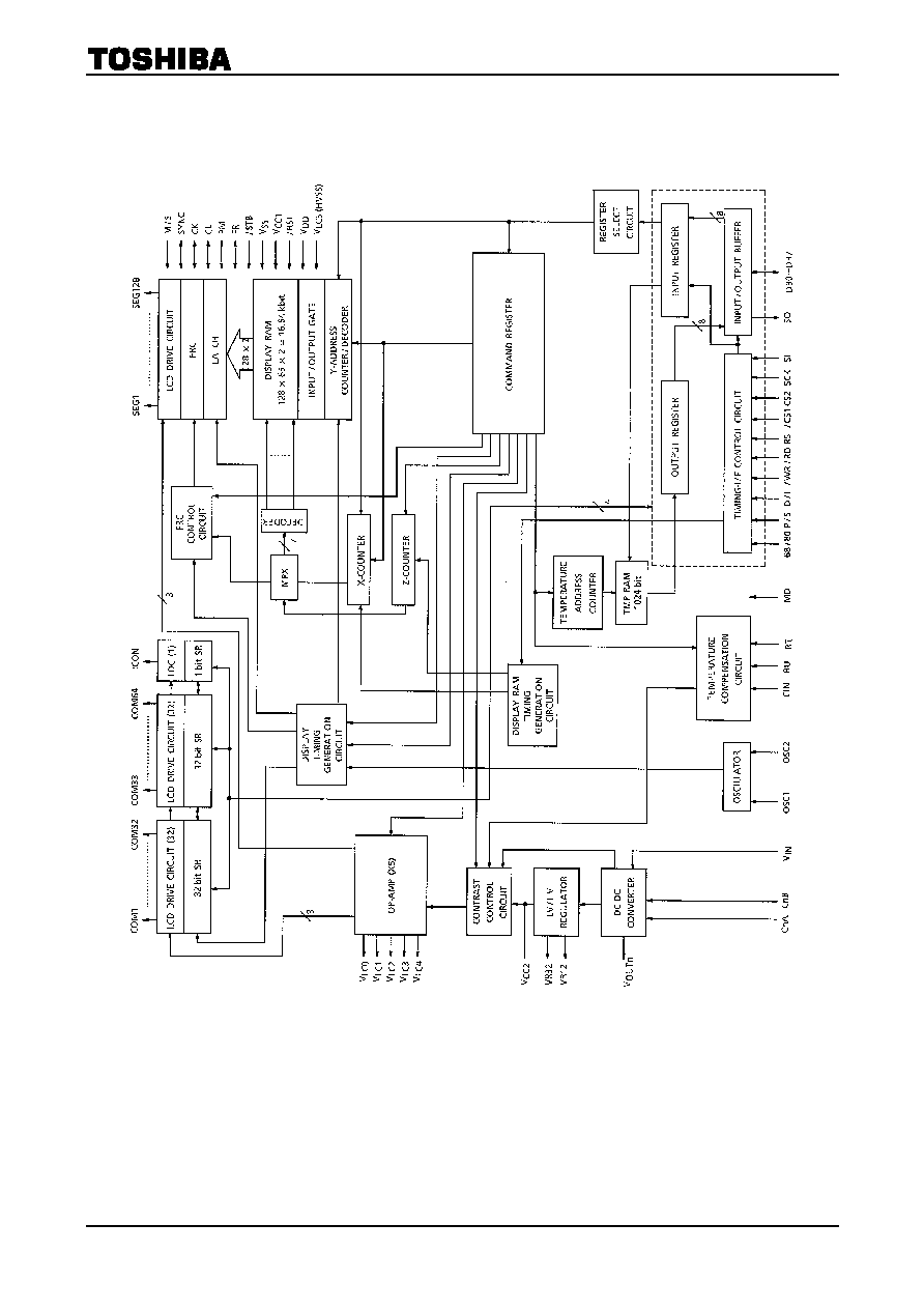
B
l
ock D
i
agr
a
m
T6K14
2002-01-16
3
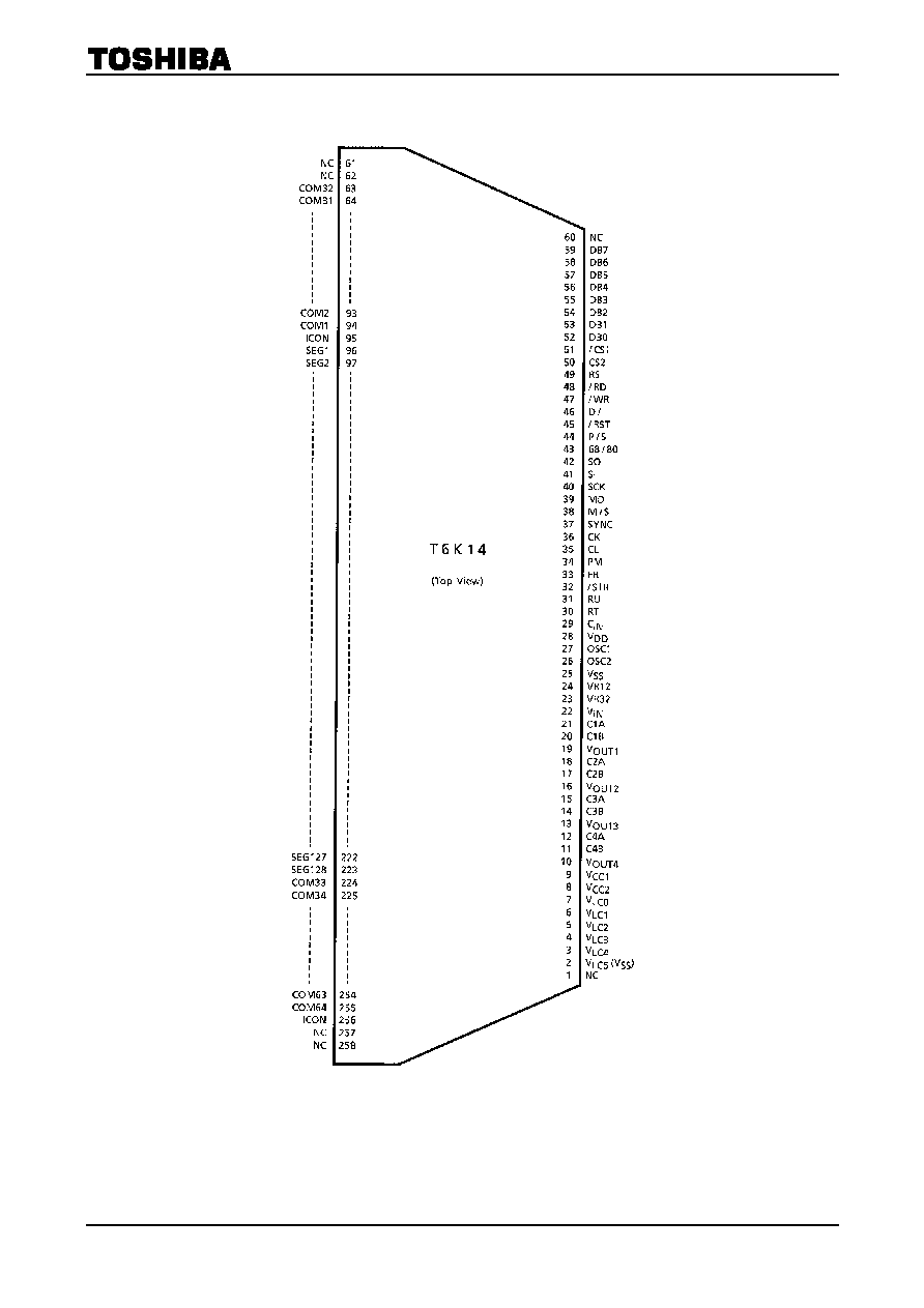
Pin Configuration
Note: Above drawing describes pin configuration of the LSI Chip, it doesn't define the tape carrier package.

T6K14
2002-01-16
4
PAD Specification
Item Size
Unit
Chip Size
8960◊5050
µm
(1)
-4480, -2525
(2)
-4480, 2525
(3)
4480, 2525
Chip Tip Coordinates
(4)
4480,
-2525
µm
Bump Pitch
70 (Min)
µm
Bump Height
15 (Typ.)
µm
Item Number
of
Pins
Input Pin
114 (Including dummy pins)
Output Pin
208 (Including dummy pins)
FUSE Pin
12
(Note 1)
TEST Pin
19
(Note 1)
Note 1: FUSE (No.115 to 126) and TEST (No.335 to 353) are LSI test pins, leave these pins open.

T6K14
2002-01-16
5
Pad Layout

T6K14
2002-01-16
6
Pad Coordinates
[Unit: µm]
No. Name X-Point Y-Point
No. Name X-Point
Y-Point
No.
Name X-Point Y-Point
1 DUMMY1 -4203
-2293 48
V
IN
-737
-2293 95
/RD 2719 -2293
2 V
LC2
-4121
-2293 49 DUMMY11
-665
-2293 96
V
SS
2791
-2293
3 V
LC2
-4049
-2293 50 DUMMY12
-521
-2293 97
RS 2863 -2293
4 DUMMY2 -3977
-2293 51 VR32
-449
-2293 98
V
DD
2935
-2293
5 V
LC1
-3905
-2293 52 VR32
-377
-2293 99
CS2 3007 -2293
6 V
LC1
-3833
-2293 53 VR12
-305
-2293 100
/CS1 3079 -2293
7 DUMMY3 -3761
-2293 54 VR12
-233
-2293 101
V
SS
3151
-2293
8 V
LC0
-3689
-2293 55
V
SS
-161
-2293 102
DB0 3223 -2293
9 V
LC0
-3617
-2293 56
V
SS
-89
-2293 103
DB1 3295 -2293
10 DUMMY4 -3545
-2293 57
V
SS
-17
-2293 104
DB2 3367 -2293
11 DUMMY5 -3401
-2293 58
V
SS
55
-2293 105
DB3 3439 -2293
12 V
CC2
-3329
-2293 59
V
SS
127
-2293 106
DB4 3511 -2293
13 V
CC2
-3257
-2293 60 DUMMY13
199
-2293 107
DB5 3583 -2293
14 DUMMY6 -3185
-2293 61 OSC2
271
-2293 108
DB6 3655 -2293
15 DUMMY7 -3113
-2293 62 DUMMY14
343
-2293 109
DB7 3727 -2293
16 DUMMY8 -3041
-2293 63 OSC1
415
-2293 110 DUMMY16 3799 -2293
17 DUMMY9 -2969
-2293 64 DUMMY15
487
-2293 111 DUMMY17 3871 -2293
18 V
CC1
-2897
-2293 65
V
DD
559
-2293 112 DUMMY18 3943 -2293
19 V
CC1
-2825
-2293 66
V
DD
631
-2293 113 DUMMY19 4015 -2293
20 V
CC1
-2753
-2293 67
V
DD
703
-2293 114 DUMMY20 4097 -2293
21 V
CC1
-2681
-2293 68
V
DD
775
-2293 115
FUSE25 4280 -2129
22 DUMMY10 -2609
-2293 69
C
I
N
847
-2293 116
FUSE24 4280 -1994
23 V
OUT4
-2537
-2293 70
RT
919
-2293 117
FUSE2G 4280 -1869
24 V
OUT4
-2465
-2293 71
RU
991
-2293 118
FUSE23 4280 -1744
25 C4B -2393
-2293 72
V
DD
1063
-2293 119
FUSE22 4280 -1619
26 C4B -2321
-2293 73 /STB
1135
-2293 120
FUSE21 4280 -1494
27 C4A -2249
-2293 74
FR
1207
-2293 121
FUSE35 4280 -1369
28 C4A -2177
-2293 75
PM
1279
-2293 122
FUSE34 4280 -1244
29 V
OUT3
-2105
-2293 76
CL
1351
-2293 123
FUSE3G 4280 -1119
30 V
OUT3
-2033
-2293 77
CK
1423
-2293 124
FUSE33 4280 -994
31 C3B -1961
-2293 78 SYNC
1495
-2293 125
FUSE32 4280 -869
32 C3B -1889
-2293 79
V
SS
1567
-2293 126
FUSE31 4280 -744
33 C3A -1817
-2293 80
M/S
1639
-2293 127 DUMMY21 4280 -619
34 C3A -1745
-2293 81
V
DD
1711
-2293 128
COM32 4280 -468
35 V
OUT2
-1673
-2293 82
MD
1783
-2293 129
COM31 4280 -398
36 V
OUT2
-1601
-2293 83
V
SS
1855
-2293 130
COM30 4280 -328
37 C2B -1529
-2293 84
SCK
1927
-2293 131
COM29 4280 -258
38 C2B -1457
-2293 85
SI
1999
-2293 132
COM28 4280 -188
39 C2A -1385
-2293 86
SO
2071
-2293 133
COM27 4280 -118
40 C2A -1313
-2293 87
V
DD
2143
-2293 134
COM26 4280 -48
41 V
OUT1
-1241
-2293 88 68/80
2215
-2293 135
COM25 4280 22
42 V
OUT1
-1169
-2293 89
V
SS
2287
-2293 136
COM24 4280 92
43 C1B -1097
-2293 90
RS
2359
-2293 137
COM23 4280 162
44 C1B -1025
-2293 91
V
DD
2431
-2293 138
COM22 4280 232
45 C1A -953
-2293 92 /RST
2503
-2293 139
COM21 4280 302
46 C1A -881
-2293 93
D/I
2575
-2293 140
COM20 4280 372
47 V
IN
-809
-2293 94
/WR
2647
-2293 141
COM19 4280 442

T6K14
2002-01-16
7
[Unit: µm]
No. Name X-Point
Y-Point
No. Name X-Point
Y-Point
No.
Name X-Point
Y-Point
142 COM18 4280
512
189 SEG29 2486
2325 236
SEG76 -804 2325
143 COM17 4280
582
190 SEG30 2416
2325 237
SEG77 -874 2325
144 COM16 4280
652
191 SEG31 2346
2325 238
SEG78 -944 2325
145 COM15 4280
722
192 SEG32 2276
2325 239
SEG79 -1014 2325
146 COM14 4280
792
193 SEG33 2206
2325 240
SEG80 -1084 2325
147 COM13 4280
862
194 SEG34 2136
2325 241
SEG81 -1154 2325
148 COM12 4280
932
195 SEG35 2066
2325 242
SEG82 -1224 2325
149 COM11 4280 1002
196 SEG36 1996
2325 243
SEG83 -1294 2325
150 COM10 4280 1072
197 SEG37 1926
2325 244
SEG84 -1364 2325
151 COM9 4280 1142
198 SEG38 1856 2325 245
SEG85 -1434 2325
152 COM8 4280 1212
199 SEG39 1786 2325 246
SEG86 -1504 2325
153 COM7 4280 1282
200 SEG40 1716 2325 247
SEG87 -1574 2325
154 COM6 4280 1352
201 SEG41 1646 2325 248
SEG88 -1644 2325
155 COM5 4280 1422
202 SEG42 1576 2325 249
SEG89 -1714 2325
156 COM4 4280 1492
203 SEG43 1506 2325 250
SEG90 -1784 2325
157 COM3 4280 1562
204 SEG44 1436 2325 251
SEG91 -1854 2325
158 COM2 4280 1632
205 SEG45 1366 2325 252
SEG92 -1924 2325
159 COM1 4280 1702
206 SEG46 1296 2325 253
SEG93 -1994 2325
160 ICOM1A 4280
1772
207 SEG47
1226
2325
254
SEG94 -2064 2325
161 SEG1 4280 1842
208 SEG48 1156 2325 255
SEG95 -2134 2325
162 SEG2 4280 1912
209 SEG49 1086 2325 256
SEG96 -2204 2325
163 SEG3 4280 1982
210 SEG50 1016 2325 257
SEG97 -2274 2325
164 SEG4 4280 2052
211 SEG51 946 2325 258
SEG98 -2344 2325
165 SEG5 4280 2133
212 SEG52 876 2325 259
SEG99 -2414 2325
166 SEG6 4107 2325
213 SEG53 806 2325 260
SEG100 -2484 2325
167 SEG7 4026 2325
214 SEG54 736 2325 261
SEG101 -2554 2325
168 SEG8 3956 2325
215 SEG55 666 2325 262
SEG102 -2624 2325
169 SEG9 3886 2325
216 SEG56 596 2325 263
SEG103 -2694 2325
170 SEG10 3816 2325
217 SEG57
526
2325 264
SEG104 -2764 2325
171 SEG11 3746 2325
218 SEG58
456
2325 265
SEG105 -2834 2325
172 SEG12 3676 2325
219 SEG59
386
2325 266
SEG106 -2904 2325
173 SEG13 3606 2325
220 SEG60
316
2325 267
SEG107 -2974 2325
174 SEG14 3536 2325
221 SEG61
246
2325 268
SEG108 -3044 2325
175 SEG15 3466 2325
222 SEG62
176
2325 269
SEG109 -3114 2325
176 SEG16 3396 2325
223 SEG63
106
2325 270
SEG110 -3184 2325
177 SEG17 3326 2325
224 SEG64
36
2325 271
SEG111 -3254 2325
178 SEG18 3256 2325
225 SEG65
-34 2325 272
SEG112
-3324 2325
179 SEG19 3186 2325
226 SEG66 -104 2325 273
SEG113
-3394 2325
180 SEG20 3116 2325
227 SEG67 -174 2325 274
SEG114
-3464 2325
181 SEG21 3046 2325
228 SEG68 -244 2325 275
SEG115
-3534 2325
182 SEG22 2976 2325
229 SEG69 -314 2325 276
SEG116
-3604 2325
183 SEG23 2906 2325
230 SEG70 -384 2325 277
SEG117
-3674 2325
184 SEG24 2836 2325
231 SEG71 -454 2325 278
SEG118
-3744 2325
185 SEG25 2766 2325
232 SEG72 -524 2325 279
SEG119
-3814 2325
186 SEG26 2696 2325
233 SEG73 -594 2325 280
SEG120
-3884 2325
187 SEG27 2626 2325
234 SEG74 -664 2325 281
SEG121
-3954 2325
188 SEG28 2556 2325
235 SEG75 -734 2325 282
SEG122
-4024 2325

T6K14
2002-01-16
8
[Unit: µm]
No. Name X-Point Y-Point
No. Name X-Point
Y-Point
No.
Name X-Point Y-Point
283 SEG123 -4105 2325
307
COM51 -4280 512 331
V
LC3
-4280
-1797
284 SEG124 -4280 2133
308
COM52 -4280 442 332
V
LC3
-4280
-1869
285 SEG125 -4280 2052
309
COM53 -4280 372 333
DUMMY25
-4280
-1994
286 SEG126 -4280 1982
310
COM54 -4280 302 334
DUMMY26
-4280
-2119
287 SEG127 -4280 1912
311
COM55 -4280 232 335
TEG1 2249 -450
288 SEG128 -4280 1842
312
COM56 -4280 162 336
TEG2 2349 -450
289 COM33 -4280 1772
313
COM57 -4280 92 337
TEG3 2449 -450
290 COM34 -4280 1702
314
COM58 -4280 22 338
TEG4 2588 -450
291 COM35 -4280 1632
315
COM59 -4280
-48 339
TEG5 2688 -450
292 COM36 -4280 1562
316
COM60 -4280
-118 340
TEG6 2788 -450
293 COM37 -4280 1492
317
COM61 -4280
-188 341
TEG7 2249 -301
294 COM38 -4280 1422
318
COM62 -4280
-258 342
TEG8 2349 -301
295 COM39 -4280 1352
319
COM63 -4280
-328 343
TEG9 2449 -301
296 COM40 -4280 1282
320
COM64 -4280
-398 344
TEG10 -2448 1172
297 COM41 -4280 1212
321
ICOM1B
-4280
-468 345
TEG11 -2448 1072
298 COM42 -4280 1142
322
DUMMY22
-4280
-619 346
TEG12 -2448 972
299 COM43 -4280 1072
323 V
LC5
-4280
-744 347
TEG13 -2448 872
300 COM44 -4280 1002
324 V
LC5
-4280
-869 348
TEG14 -2448 699
301 COM45 -4280 932
325
V
LC5
-4280
-994 349
TEG15 -2448 599
302 COM46 -4280 862
326
V
LC5
-4280
-1119 350
TEG16 -2448 499
303 COM47 -4280 792
327
DUMMY23
-4280
-1244 351
TEG17 -2448 399
304 COM48 -4280 722
328
V
LC4
-4280
-1369 352
TEG18 -2448 201
305 COM49 -4280 652
329
V
LC4
-4280
-1441 353
TEG19 -2448 101
306 COM50 -4280 582
330
DUMMY24
-4280
-1619

T6K14
2002-01-16
9
Pin Function
(1)
Pin Name
I/O
Function
SEG1 to SEG128
Output
LCD drive column (segment) signals
COM1 to COM64
Output
LCD drive row (common) signals
ICON
Output
LCD drive row (common) signals for icon
DB0 to DB7
I/O
Data bus
/CS1 Input
Input for chip select signal
Data write : Data write enable at the rising edge of /CS1.
Data read : Data read out while /CS1 is in Low level.
CS2 Input
Input for chip select signal
Data write : Data write enable at the falling edge of CS2.
Data read : Data read out while CS2 is in High level.
D/I Input
Input for Data/Instruction select signal
D/I = H Indicates that the data on DB0 to DB7 or SI is the display data.
D/I = L Indicates that the data on DB0 to DB7 or SI is the instruction data.
/WR Input
Input for write enable signal
/WR = L State of select
/RD Input
Input for read enable signal
/RD = L State of select
RS
Input
Input for register/mode select signal
P/S Input
Input for parallel interface/serial interface select signal
P/S = H Parallel interface is selected. SI and SCK must be connected to V
DD
or
V
SS
.
P/S = L Serial interface is selected. DB0 to DB7, /WR and/RD must connected to
V
DD
or V
SS
.
68/80 Input
Input for 68 series MPU/80 series MPU select signal
68/80 = H 68 series MPU selected
68/80 = L 80 series MPU selected
SO
Output
Output for serial data
SI
Input
Input for serial data
SCK
Input
Input for serial clock
/RST Input
Input for reset signal
/RST = L State of select

T6K14
2002-01-16
10
Pin Function
(2)
Pin Name
I/O
Function
/STB Input
Input for standby signal
Usually connected to V
DD
/STB = L T6K14 is the state of standby.
Column and row drive signal is V
SS
level, and on-chip oscillator is
stop.
OSC1, OSC2
I/O
When using a internal clock oscillator, connect a resistor between OSC1 and OSC2.
When using a external clock, input the clock to OSC1 and leave OSC2 open.
V
IN
Power supply for DC-DC converter
CIN
I/O
Input for clock of temperature compensation
RU
Connect with standard resistor
RT
Connect
with
thermistor
C1A, C1B
Connect with capacitance for ◊2 mode
V
OUT1
DC-DC converter output terminal (◊2 level)
C2A, C2B
Connect with capacitance for ◊3 mode
V
OUT2
DC-DC converter output terminal (◊3 level)
C3A, C3B
Connect with capacitance for ◊4 mode
V
OUT3
DC-DC converter output terminal (◊4 level)
C4A, C4B
Connect with capacitance for ◊5 mode
V
OUT4
DC-DC converter output terminal (◊5 level)
VR12
LV regulator monitor terminal
(Note)
VR32
LV regulator monitor terminal
(Note)
V
CC1
Power supply for LCD driver circuit
V
CC2
Power supply for HV regulator monitor terminal
(Note)
V
LC0
to V
LC5
Power supply for LCD driver circuit
VLC5 terminal is connect to V
SS
. (Note)
V
SS
, V
DD
Power supply for logic circuit. Ground: Reference
Note: Connect the capacitance between this terminal and V
SS
.

T6K14
2002-01-16
11
Pin Function
(3)
Pin Name
I/O
Function
MD
Input
Mode detect pin for Status Read
M/S Input
Input for master/slave selects
M/S = H T6K14 is master chip
M/S = L T6K14 is slave chip
CL I/O
Input/Output for shift clock pulse
Master mode (M/S = H) output
Slave mode (M/S = L) input
PM I/O
Input/Output for frame signal
Master mode (M/S = H) output
Slave mode (M/S = L) input
FR I/O
Input/Output for display synchronous signal
Master mode (M/S = H) output
Slave mode (M/S = L) input
SYNC I/O
Input/Output for grayscale signal data
Master mode (M/S = H) output
Slave mode (M/S = L) input
CK I/O
Input/Output for grayscale signal data
Master mode (M/S = H) output
Slave mode (M/S = L) input
Pin Function
(4)
PS
68/80 Interface
Type /CS1
CS2
D/I
RS
/WR
/RD
SO
SI
SCK
DB0
to
DB7
80 series MPU (/CS1)
/CS1
H
A0
A1
/WR
/RD
Open
L/H
L/H
DB0 to DB7
L
80 series MPU (CS2)
L
CS2
A0
A1
/WR
/RD
Open
L/H
L/H
DB0 to DB7
H
H
68 series MPU
L
H
A0
A1
R/W
E
Open
L/H
L/H
DB0 to DB7
L L/H
Serial
interface
L H L/H
L/H
L/H
L/H
SO
SI SCK Open
Note: H denotes the V
DD
level; L denotes the V
SS
level.

T6K14
2002-01-16
12
Function of Each Block
Interface logic
The T6K14 can be operated with 80 series MPUs or 68 series MPUs or Serial Interface.
Fig. 1 shows an example of interface. For details, please refer to the example interface part of application
circuit.
Fig. 1
Fig. 2
Input register
The register stores 8 bit data from MPU. D/I signal discriminate between command data and display data.
X-address counter
X-address counter is 64-Up/Down counter. It holds the row address for the display RAM. Then it is selected
by the command, writing to or reading the data of display RAM causes the X-address to automatically
increment or decrement.
Y (Page) -address counter
The Y (Page) -address counter is 32-Up/Down counter. It holds the column address for the display RAM. This
counter is selected by the command. Writing to or reading the display RAM causes the Y-address to
automatically increment or decrement.
Z-address counter
The Z-address counter is 64-Up counter that provide the display RAM data for the LCD drive circuit. The
data stored in Z-Address Register is send to Z-Address counter as Z start address.
For instance, when Z start address is 16, the counter increment like this: 16, 17, 18∑∑∑, 62, 63, 0, 1, 2∑∑∑14, 15,
16. Therefore, the display start line is 16-line of the display RAM.

T6K14
2002-01-16
13
Up/Down register
The 1 bit data stored in this register selects Up or Down mode of X and Y (Page) -address counter.
Counter select register
The 1 bit data stored in this register selects X-address counter or Y (Page) -address counter.
Display ON/OFF register
This 1 bit register holds the display ON or OFF state. In the OFF state, the output data from the display
RAM is not selected. In the On state, the display data appears according to the display RAM data. The
display ON or OFF state does not affect the data of display RAM.
Z-address register
This 6 bits register holds the data that indicates the display start line.
Oscillator
The T6K14 has an on-chip oscillator. When using this oscillator, connect an external resistor between OSC1
and OSC2. When using external clock, input the clock to OSC1 and open OSC2, as shown in Fig. 3.
Fig. 3
Timing generation circuit
The circuit divides the signals from the oscillator and generates display timing signals and operating clock.
Shift-register
The T6K14 has two 32 bits shift-register and shift register of ICON. These shift-register construct 65 bits
shift-register.
Latch circuit
This latch circuit latches the data from the display RAM.

T6K14
2002-01-16
14
Column driver circuit
Column driver circuit consists of 128 driver circuits. One of the four LCD driving level is selected by the
combination of M (internal signal) and the display data transferred from the latch circuit. Details of column
driver circuit are shown in Fig. 4.
Fig. 4
Row driver circuit
Row driver circuit consists of 65 drive circuits. One of the four LCD driving level is selected by the
combination of M (internal signal) and the data from the sift register. Details of row driver circuit are shown
in Fig. 5.
Fig. 5
T6K14
2002-01-16
15
DC-DC converter
The T6K14 built in DC-DC converter circuit 2/3/4/5 times.
V
outn
= 0 (V
SS
level) is at the time of /RST = L or /STB = L.
The capacitor for DC-DC converter and the capacitor for DC-DC level maintenance usually use about 1.0µF.
Since the power supply V
IN
terminal for DC-DC converter circuit can input voltage usually higher than a
digital system power supply V
DD
terminal, it can generate required LCD voltage in a DC-DC converter.
However, since the maximum of LCD operation voltage is 16.5 V (max) be careful about the relation of the
voltage conditions (V
IN
voltage) and the number of the DC-DC steps which are used in a DC-DC converter so
that the DC-DC converted voltage (voltage value outputted from Vout) does not exceed 16.5 V.
Note 1: Power supply voltage ........ 3.3 V V
IN
2.7 V, V
IN
V
DD
Note 2: LCD voltage ................... 16.5 V V
IN
◊ n
(n: number of DC-DC steps)
ex) Using the ◊5 mode
About Terminal Processing
Conditions C1A,
C1B
V
OUT1
C2A,
C2B
V
OUT2
C3A,
C3B
V
OUT3
C4A,
C4B V
OUT4
◊2
mode
O
O Open Open Open Open Open Open
◊3
mode
O O O O
Open
Open
Open
Open
◊4
mode
O O O Open O O Open
Open
◊5
mode
O O O
Open
O
Open
O O
None
Open Open Open Open Open Open Open Open
Note: O = Connect the capacitance.
Note: The voltage outputted from DC-DC converter changes with voltage condition, temperature environment,
substrate environment, etc.

T6K14
2002-01-16
16
Voltage driver resistor, contrast control circuit
(Normal mode)
The T6K14 has on-chip resistors to divide bias voltage with op-amp., and a contrast control circuit.
The voltage bias is changed by instruction command. And one of four bias is selected.

T6K14
2002-01-16
17
Contrast control circuit
(Power Save Mode)
Contrast control output voltage
(VLC0)
(Typical Value)
Condition VR32
[V]
V
LC0
(min)
[V]
V
LC0
(max)
[V]
Contrast Step
[mV]
Bias
Power Save
3.2
2.2
5.0
11.0
1/12

T6K14
2002-01-16
18
Temperature compensation circuit
The T6K14 has the temperature compensation circuit.
While this temperature compensation circuit detects temperature, it controls automatically built-in contrast
control. And, original contrast control suitable for all LCD material can be created by writing data in RAM
for temperature compensation circuit (TMP-RAM). Please refer to description of a function about the usage.

T6K14
2002-01-16
19
Command Definition
Command
Reg.
No.
D/I
RS
/WR
/RD
DB7
DB6
DB5 DB4 DB3 DB2 DB1
DB0
Register set (REG)
0 0 0 1 0 0 0
Register
(0
to
31)
Status read (STRD)
0 0 1 0 MD
*
TMP HVR
N/F
DP
Y/X
U/D
Data
mode
(DMD)
R0 0 1 0 1 0 0 0 0 0
D/TM
Y/X
U/D
Display
mode
(DPE)
R1 0 1 0 1 0 CDR SDR
0 0 0
N/F
DP
Power mode (PWE)
R2
0
1
0
1
◊4/◊5
0
0
0
0
VR
OP
DC
Duty/Bias Select (DTE)
R3
0
1
0
1
Bias (5 to 9)
0
0
Duty (0 to
3)
Oscillation
(OSE)
R4 0 1 0 1 0 0 0 0 0 0 0
OSC
1
F/N
X-Address (0 to 63)
X, Y-address
(SXYE)
R5 0 1 0 1
0 0 0
Y-Address
(0
to
31)
Z-address
(SZE)
R6 0 1 0 1 0 0
Z-Address
(0
to
63)
Contrast control (SCE)
R7
0
1
0
1
Contrast Control (0 to 255)
TMP
mode
(TMPM)
R8 0 1 0 1 0 0 0 0
TMO
F
0
time (0 to 3)
TMP-RAM address (TMPA)
R9
0
1
0
1
0
TMP-RAM address (0 to 127)
FRS control mode (FRSC)
R10
0
1
0
1
0
0
FR control (0 to 63)
R11 0 1 0 1
Grayscale (1) (GR1)
Normal display pattern
R12 0 1 0 1
Grayscale pattern data (1)
Normal display data = "00" ∑∑∑ 16 bits
R13 0 1 0 1
Grayscale (2) (GR2)
Normal display pattern
R14 0 1 0 1
Grayscale pattern data (2)
Normal display data = "01" ∑∑∑ 16 bits
R15 0 1 0 1
Grayscale (3) (GR3)
Normal display pattern
R16 0 1 0 1
Grayscale pattern data (3)
Normal display data = "10" ∑∑∑ 16 bits
R17 0 1 0 1
Grayscale (4) (GR4)
Normal display pattern
R18 0 1 0 1
Grayscale pattern data (4)
Normal display data = "11" ∑∑∑ 16 bits
R19 0 1 0 1
Grayscale (5) (GR5)
Power save display pattern
R20 0 1 0 1
Grayscale pattern data (5)
Power save display data = "00" ∑∑∑ 16 bits
R21 0 1 0 1
Grayscale (6) (GR6)
Power save display pattern
R22 0 1 0 1
Grayscale pattern data (6)
Power save display data = "01" ∑∑∑ 16 bits
R23 0 1 0 1
Grayscale (7) (GR7)
Power save display pattern
R24 0 1 0 1
Grayscale pattern data (7)
Power save display data = "10" ∑∑∑ 16 bits
R25 0 1 0 1
Grayscale (8) (GR8)
Power save display pattern
R26 0 1 0 1
Grayscale pattern data (8)
Power save display data = "11" ∑∑∑ 16 bits
TMP-RAM address read
R27
0
1
1
0
*
TMP-RAM address data (7 bits)
Test mode
R28 to
31
0
1
0
1
Please do not using this register
Data write (DAWR)
1 1 0 1
Write
data
Data read (DARD)
1 1 1 0
Read
data

T6K14
2002-01-16
20
Register set
Identify register number
R0 (00H) to R31 (1FH)
Note: R28 to R31 registers are provided for test. Please do not choose these registers.
R0: Data mode
D/TM : Selects between display RAM address and TMP-RAM address counters.
D/TM = 1: Display RAM counter is selected. D/TM = 0: TMP-RAM counter is selected.
Y/X
: Selects between X-counter and Y-counter.
Y/X = 1: Y-counter is selected.
Y/X = 0: X-counter is selected.
U/D
: Sets a counter mode.
U/D = 1: Up mode is selected.
U/D = 0: Down mode is selected.
R1: Display mode
CDR
: Sets the common data scanning direction.
CDR = 1: COM1 COM64 ICON
CDR = 0: COM64 COM1 ICON
SDR
: Sets the segment data direction
See "RAM map and CDR, SDR relation"
N/F
: Selects between normal display mode and Power save mode.
N/F = 1: Normal display mode is selected. N/F = 0: Power save mode (Flag display only) is selected.
DP
: Turns display ON or OFF.
DP = 1: Display is turned ON.
DP = 0: Display is turned OFF.

T6K14
2002-01-16
21
R2: Power management
X4/X5 :
X4/X5 = 0: LCD voltage regulator output voltage is 12.5 V typ. (at Ta = 25∞C)
X4/X5 = 1: LCD voltage regulator output voltage is 11.0 V typ. (at Ta = 25∞C)
VR
: LCD voltage regulator (HVR)
VR = 1: Voltage regulator is turned ON.
VR = 0: Voltage regulator is turned OFF.
Input the voltage to V
CC2
pin.
OP :
Op-amp
OP = 1: Op-amp is turned ON.
OP = 0: Op-amp is turned OFF.
Input various voltage to V
LC0
to V
LC4
pins.
DC :
DC-DC
converter
DC = 1: DC-DC converter is turned ON.
DC = 0: DC-DC converter is turned OFF.
Input the voltage to V
CC1
pin.
Note: Refer to the description of a function for the combination of a power supply setup.
R3: Bias/Duty select
(Note): The T6K14¥s COM output which corresponds to the line of LCD is changed by the Duty.
When CDR = 1, COM outputs in each Duty are shown below.
1/n duty
LCD
1
st
line, 2
nd
line,
∑ ∑ ∑ ∑ ∑ ∑ ∑ ∑ ∑ ∑ ∑ ∑ ∑ ∑ ∑ ∑ ∑ ∑ ∑ ∑ ∑
, n
th
line, ICON
1/65 duty
COM1, COM2,
∑ ∑ ∑ ∑ ∑ ∑ ∑ ∑ ∑ ∑ ∑
,COM32, COM33, COM34,
∑ ∑ ∑ ∑ ∑ ∑
,COM64, ICON
1/57 duty
COM1, COM2,
∑ ∑ ∑ ∑ ∑ ∑ ∑ ∑ ∑
,COM28, COM33, COM34,
∑ ∑ ∑ ∑ ∑ ∑
,COM60, ICON
1/49 duty
COM1, COM2,
∑ ∑ ∑ ∑ ∑ ∑ ∑
,COM24, COM33, COM34,
∑ ∑ ∑ ∑ ∑ ∑
,COM56, ICON
1/35 duty
COM1, COM2,
∑ ∑ ∑ ∑ ∑
,COM17, COM33, COM34,
∑ ∑ ∑ ∑ ∑ ∑
,COM49, ICON
R4: Oscillator control
OSC :
Oscillator
OSC = 1: Oscillator is turned ON.
OSC = 0: Oscillator is turned OFF.
Input an external clock to OSC1 pin.

T6K14
2002-01-16
22
R5: X-address, Y-address set
(1) X-address set
F/N = 0: Sets display RAM address (in the range 0 to 63
(Note)
).
F/N = 1: Sets flag RAM (The data from DB0 to DB5 is ignored)
Note: Since the effective range of X-address changes by duty setup, pleace be careful.
(2) Y-address set
R6: Z-address set
This command sets a Z-address. The display RAM and flag RAM are separated and only the display RAM is
selected. By selecting any address in the column direction of the display RAM, it is possible to set the first
line on the LCD screen. The display data can be scrolled in the vertical direction by setting the first line in
this way.
Since the effective range of Z-address changes by duty setup, please be careful.
Please refer to description of a function for details.
R7: Contrast control
This command sets contrast.
It becomes the maximum contrast when data is 255, and it becomes the minimum contrast when data is 0.
When a temperature compensation circuit is used, data for a contrast control circuit are changed to the sum
of R7 register 8-bit data and TMP-RAM 8-bit data. Therefore, the contrast is controlled.
R8: TMP mode
TMOF: Temperature compensation ON/OFF
TMOF = 1: ON
TMOF = 0: OFF (Note 1)
Note 1: Data on the output bus of the temperature table RAM are
fixed on Low data. Therefore, data on the contrast control
register are inputted to contrast control circuit.

T6K14
2002-01-16
23
R9: TMP-RAM address
This command sets TMP-RAM address.
In case of using this command, counter up mode only.
R10: FRS control
This command sets the number of the row lines for polarity change.
The setting of FRS corresponds to the row line number, see following table.
FRS Frame
0
In case 1/x duty is selected by R3, FR signal inverts on every x line.
(Note)
n
FR signal inverts on every (n + 1) line.
Note: In case FRS = 0;
FR signal inverts synchronously with the earlier edge of COM1.
In case FRS 0 (1 to 63);
FR signal inverts synchronously with the edge of COMm. (m = 1 to 64, or ICON)
"m" shows a COM line right after the instruction practice.
R11 to R26: Grayscale data
This register have the PWM (Pulse Width Modulation) and FRC (Frame Rate Control) control data. PWM
chooses one of 10 kinds and assigns data of PWM to four frames.
This register is constituted from "0th FR data" by 4 bits of "3rd FR data", and inputs PWM data into four FR
data. That is, it becomes data of one color (one grayscale level) by 4 frames.
Display Mode
Display RAM Data
Register No.
Grayscale Data
0
0
R11, 12
4 bits ◊ 4
0
1
R13, 14
4 bits ◊ 4
1
0
R15, 16
4 bits ◊ 4
Normal Display Mode
1
1
R17, 18
4 bits ◊ 4
0
0
R19, 20
4 bits ◊ 4
0
1
R21, 22
4 bits ◊ 4
1
0
R23, 24
4 bits ◊ 4
Power Save Mode
1
1
R25, 26
4 bits ◊ 4

T6K14
2002-01-16
24
Data of PWM
(Pulse Width Modulation)
*:
The phase of PWM turn over by the even/odd of the output pin.
Note: This area is selected to off level (0/9 level)
R27: TMP-RAM address read
This register stores the address equivalent to the temperature detected by the temperature compensation
circuit. (Read out only). When the temperature compensation circuit is used, the contrast is controlled by the
sum of TMP-RAM data specified by this address, and the data in the R7 register.
R28 to 31: Test mode
Please don' t access this register.

T6K14
2002-01-16
25
Status read
MD : When MD terminal is connected to V
DD
level, MD (DB7) = 1.
When MD terminal is connected to V
SS
level, MD (DB7) = 0.
TMP : When TMP = 1, the temperature compensation circuit is turned ON.
When TMP = 0, the temperature compensation circuit is turned OFF.
HVR : When HVR = 1, HV - Regulator X 4 mode is selected.
When HVR = 0, HV - Regulator X 5 mode is selected.
N/F : When N/F = 1, Normal display mode is selected.
When N/F = 0, Power save mode (FLAG display only) is selected.
DP : When DP = 1, Display is turned ON.
When DP = 0, Display is turned OFF.
Y/X : When Y/X = 1, Y - counter is selected.
When Y/X = 0, X - counter is selected.
U/D : When U/D = 1, X and Y counters are in up mode.
When U/D = 0, X and Y counters are in down mode.
Write/read data
(DAWR/DARD)
The command DAWR writes 8-bit data to Display RAM or TMP-RAM.
The command DARD reads 8-bit data from Display RAM or TMP-RAM.

T6K14
2002-01-16
26
Function Description
Display data bit
SDR = 1
SDR = 0
Display mode

T6K14
2002-01-16
27
RAM map and CDR, SDR relation
(1) CDR = 1, SDR = 1
(2) CDR = 1, SDR = 0
(3) CDR = 0, SDR = 1
(4) CDR = 0, SDR = 0

T6K14
2002-01-16
28
Reset function
When/RST = L, reset function is executed and following instruction (resister) are executed.
Command Reg
No.
DB7
DB6
DB5
DB4
DB3
DB2
DB1
DB0
Data
mode
R0 * * * * * 1 1 1
Display
mode
R1 * 1 1 * * * 1 0
Power
mode
R2 1 * * * * 0 0 0
Duty/Bias
R3 1 0 0 1 * * 1 1
Oscillator
R4 * * * * * * * 1
X, Y-address
R5 0 0 0 0 0 0 0 0
Z-address
R6 * * 0 0 0 0 0 0
Contrast
control
R7 0 0 0 0 0 0 0 0
TMP
mode
R8 * * * * 0 * 0 0
TMP-RAM
address
R9 * 0 0 0 0 0 0 0
FRS
control
mode
R10 * * 0 0 0 0 0 0
Gray scale
R11 to
R27
0 0 0 0 0 0 0 0
Standby function
When/STB = L, the T6K14 is in standby state. The internal oscillation is stopped, power consumption is
reduced, and power supply for LCD (V
LC0
to V
LC5
) become V
SS
.

T6K14
2002-01-16
29
Expansion function
The T6K14 has expansion function. When using this function, the T6K14 (2 chip) can drive 256 ◊ 64 + icon
dots LCD panel (maximum) or 128 ◊ 128 + icon dots LCD panel (Maximum).
Next table shows the selectable function by using M/S pins.
M/S
H L
One chip mode Disable expansion
model
Two chips mode (Master chip)
Timing signal and power voltage
supply to Slave chip.
Two chips mode (Slave chip)
Timing signal and power voltage
are supplied from Master chip.
Fig. 6 and Fig.7 illustrate the application example of disable expansion mode and enable expansion mode.
In enable expansion mode (Tow chip mode)
As shown in Fig.7-1, Fig.7-2 Master chip supplies LCD drive signals and power voltage to slave chip. (The
oscillator, the timing circuits, Op-amp, and Contrast control circuit are disable.)
(1) Disable expansion mode
Fig. 6

T6K14
2002-01-16
30
(2) Enable expansion mode
Fig. 7-1
Fig. 7-2

T6K14
2002-01-16
31
X-address counter and Y (Page) -address counter
Fig. 8-1 shows a sample of operating procedure for the X-address counter.
After reset is executed, X-address becomes X-address = 0, then select X-counter/Up mode. Next set the X
-address to 62 by commanding SXYE (R5).
After data has been written to or read, the X-address is automatically incremented by one.
After X-counter/Down mode has been selected and data has been written to or read, the X-address is
automatically decremented by one.
When the X-counter is selected, Y-counter does not count up or down.
And flag-counter does not count up or down too.
Fig. 8-1
Fig. 8-2 shows a sample operating procedure for the Y-address counter.
After reset is executed, Y (Page) -address becomes Y-address = 0, then select Y (Page) -counter/Up -mode.
After data has been written to or read, the Y (Page) -address counter is automatically incremented by one.
After Y (Page) -counter/Down mode has been selected and data has been written to or read, the Y (Page)
-address is automatically decremented by one.
When the Y (Page) -counter is selected, X -counter doesn't count up or down.
Fig. 8-2

T6K14
2002-01-16
32
LCD Driver Waveform
(Case of normal mode)
Maximum Ratings
(Ta = 25∞C)
Item Symbol
Rating
Unit
Supply Voltage (1)
V
DD
(Note 1)
-0.3 to 7.0
V
Supply Voltage (2)
V
LC1, 2, 3, 4, 5
V
CC1
, V
CC2
V
SS
+ 18.0 to V
SS
- 0.3
V
Input Voltage
V
inp
(Note 1, 2)
-0.3 to V
DD
+ 0.3
V
Operating Temperature
Topr
-30 to 85
∞C
Storage Temperature
Tstg
-55 to 125
∞C
Note 1: Referred to V
SS
= 0 V
Note 2: Applied data bus terminals and Input terminals expect V
CC1
, V
CC2
, V
LC0
, V
LC1
, V
LC2
, V
LC3
, V
LC4
, V
LC5
.

T6K14
2002-01-16
33
Electrical Characteristics
DC Characteristics
(1) Test conditions: Unless Otherwise Noted, V
SS
= 0 V,
V
DD
= 2.4 to 3.3 V, V
IN
= 2.7 to 3.3 V, V
CC
= 6.0 to 16.5 V, Ta = 25∞C
Item Symbol
Test
Circuit
Condition Min
Typ.
Max
Unit
Applicable
Terminal
Operating Supply (1)
V
DD
2.4
3.3 V
V
DD
Operating Supply (2)
V
IN
2.7
3.3 V
V
IN
Operating Supply (3)
V
LC0
V
CC1, 2
6.0
- V
SS
16.5
- V
SS
V
V
LC0
, V
CC1
,
V
CC2
V
DD
= 2.8 to 3.3 V
0.7
V
DD
V
DD
H Level
V
IH
V
DD
= 2.4 to 2.8 V
0.8
V
DD
V
DD
V
Input Level
L Level
V
IL
0
0.2
V
DD
V
DB0 to DB7,
D/I,/WR,
/RD,/CS1,
CS2,/RST,
/STB, RS, SI,
SCK, P/S,
68/80, CL,
PM, FR,
SYNC, CK
H Level
V
OH
I
OH
= -400 µA
V
DD
- 0.2
V
DD
V
Output
Level
L Level
V
OL
I
OL
= 400 µA
0
0.2 V
DB0 to DB7,
SO, CL, PM,
FR, SYNC,
CK
Normal
Mode
Rcol1
(Note
1)
7.5 k
SEG1 to
SEG128
Column
Driver On
Resistance
Power
Save
Mode
Rcol2
(Note
2)
15.0 k
SEG1 to
SEG128
Normal
Mode
Rrow1
(Note
1)
1.5 k
COM1 to
COM64,ICON
Row Driver
On
Resistance
Power
Save
Mode
Rrow2
(Note
2)
5.0 k
COM1 to
COM64,
ICON
Input Leakage
I
IL
V
inp
= V
DD
to GND
-1
1 µA
DB0 to DB7,
D/I,/WR,
/RD,/CS1,
CS2,/RST,
/STB, RS, SI,
SCK, P/S,
68/80, CL,
PM, FR,
SYNC, CK
Operating Freq
f
OSC
(Note
7)
69 82 95 kHz
OSC1
External Clock Freq
f
ex
(Note
6)
82 kHz
OSC1
External Clock Duty
f
duty
45 50 55 %
OSC1
External Clock
Rise/Fall Time
tr/tf
50 ns
OSC1
Current Consumption
(1)
I
SS1
(Note
3)
200
350 µA
V
SS
Current Consumption
(2)
I
SS2
(Note
4)
500
700 µA
V
SS
Current Consumption
(3)
I
SSSTB
(Note
5)
-1
1 µA
V
SS
Note 1: V
SS
+ V
LC0
= 11.0 V, Load voltage = ± 0.5 V, 1/9 bias
Note 2: V
SS
+ V
LC0
= 3.0 V, Load voltage = ± 0.5 V, 1/12 bias
Note 3: V
DD
= 2.7 V, V
CC1, 2
= V
OUT4
(X5 mode), No data access, Internal clock (f
OSC
= 82 kHz), LCD out pin No
Load, 1/9 bias, 1/65 duty, op-amp. on, regulator on
Note 4: V
DD
= 3.0 V, V
CC1, 2
= V
OUT4
(X5 mode), Data access cycle f
CE
= 1 MHz, Internal clock (OSC = 82 kHz),
LCD out pin No Load, 1/9 bias, 1/65 duty, op-amp. on, regulator on
Note 5: V
DD
= 3.3 V, V
CC1, 2
- V
SS
= 16.5 V,/STB = L
Note 6: In case of 1/65 duty and f
FR
= 70 Hz
Note 7: V
DD
= 3.0 V, 1/65 duty, f
FR
= 70 Hz, Rosc = 430 k, Ta = 25∞C

T6K14
2002-01-16
34
DC Characteristics
(2)
(Test conditions: Unless Otherwise Noted, V
SS
= 0 V, V
DD
= 2.4 to 3.3 V, Ta = 25∞C)
Item Symbol
Test
Circuit
Condition Min
Typ.
Max
Unit
Applicable
Terminal
Output Voltage
(X2 Mode)
VO1 (1)
(Note
8)
4.60
5.10
V
V
OUT1
Output Voltage
(X3 Mode)
VO2 (2)
(Note
9)
6.80
7.60
V
V
OUT2
Output Voltage
(X4 Mode)
VO3 (3)
(Note
10)
9.10
10.20
V
V
OUT3
Output Voltage
(X5 Mode)
VO4 (4)
(Note
11) 11.40
12.70
V
V
OUT4
Note 8: V
IN
= 2.7 V, ILoad = 200 µA, V
CC1, 2
= 5.40 V (external power supply) CnA - CnB = 1.0 µF,
V
OUT1
- V
SS
= 1.0 µF, OSC = 82 kHz, Ta = 25∞C
Note 9: V
IN
= 2.7 V, ILoad = 200 µA, V
CC1, 2
= 8.10 V (external power supply) CnA - CnB = 1.0 µF,
V
OUT1
- V
SS
= 1.0 µF, OSC = 82 kHz, Ta = 25∞C
Note 10: V
IN
= 2.7 V, I
Load
= 200 µA, V
CC1, 2
= 10.80 V (external power supply) CnA - CnB = 1.0 µF,
V
OUT1
- V
SS
= 1.0 µF, OSC = 82 kHz, Ta = 25∞C
Note 11: V
IN
= 2.7 V, I
Load
= 200 µA, V
CC1, 2
= 13.50 V (external power supply) CnA - CnB = 1.0 µF,
V
OUT1
- V
SS
= 1.0 µF, OSC = 82 kHz, Ta = 25∞C
DC Characteristics
(3)
(Test conditions: Unless Otherwise Noted, V
SS
= 0 V, V
DD
= 2.4 to 3.3 V)
Item Symbol
Test
Circuit
Condition Min
Typ.
Max
Unit
Applicable
Terminal
X4/X5 = 0, Ta = 25∞C
(Note
12)
12.3
12.5
12.7 V
V
CC2
Regulator Reference
High Voltage (1)
VHR
X4/X5 = 1, Ta = 25∞C
(Note
12)
10.8
11.0
11.2 V
V
CC2
Regulator Reference
High Voltage (2)
VHRC
Ta
=
- 20∞C
(Note 12)
0.999
◊ VHR
1.012
◊ VHR
1.025
◊ VHR
V V
CC2
Regulator Reference
High Voltage (3)
VHRH
Ta = 60∞C
(Note 12)
0.982
◊ VHR
0.994
◊ VHR
1.006
◊ VHR
V V
CC2
Note 12: V
CC1
12.8 V at Ta = -20 to 60∞C

T6K14
2002-01-16
35
DC Characteristics
(4)
(Test conditions: Unless Otherwise Noted, V
SS
= 0 V, V
DD
= 2.4 to 3.3 V, Ta = 25∞C)
Item Symbol
Test
Circuit
Condition Min
Typ.
Max
Unit
Applicable
Terminal
Op-amp Output
Voltage Offset (1)
V
opoff
(Note
13)
-100
100 mV
V
LC0,
V
LC1
,
V
LC2
,
VLC3
,
V
LC4
Op-amp Output
Voltage Offset (2)
V
opoffs
(Note
14)
-90
90 mV
V
LC0
, V
LC1
,
V
LC2
, V
LC3
,
V
LC4
Note 13: V
DD
= 2.7 to 3.3 V, V
SS
= 0 V, 1/9 bias, 1/65 duty
V
CC1
= 13.0 V, V
CC2
= 12.5 V, Contrast control = max
Op-amp ON, DC-DC OFF, regulator OFF, LCD outpin No Load
Case
of
V
LC0
: 12.5 - V
LC0
= V
opoff
V
LC1
: (V
LC0
◊ 8/9) - V
LC1
= V
opoff
V
LC2
: (V
LC0
◊ 7/9) - V
LC2
= V
opof
f
V
LC3
: (V
LC0
◊ 2/9) - V
LC3
= V
opof
f
V
LC4
: (V
LC0
◊ 1/9) - V
LC4
= V
opoff
Note 14: V
DD
= 2.7 to 3.3 V, V
SS
= 0 V, 1/9 bias, 1/65 duty
V
CC1
= 13.0 V, V
CC2
= 12.5 V, Contrast control = max
Op-amp ON, DC-DC OFF, regulator OFF, LCD outpin No Load
V
opoffs
= ((V
LC1
- V
LC2
) - (V
LC0
- V
LC1
)) + ((V
LC3
- V
LC4
) - (V
LC4
- V
LC5
))

T6K14
2002-01-16
36
Test Circuit
(1) DC-DC converter X2 mode
(2) DC-DC converter X3 mode

T6K14
2002-01-16
37
(3) DC-DC converter X4 mode
(4) DC-DC converter X5 mode

T6K14
2002-01-16
38
AC Characteristics (1)
Switching characteristics
(80 series MPU 8
-
bit interface)
Test Conditions
(Unless Otherwise Noted,, V
SS
= 0 V, V
DD
= 2.4 to 3.3 V, Ta = 25∞C)
Item Symbol
Min
Max
Unit
Enable Cycle Time
tcycE
500
ns
Enable Pulse Width
PWEL
410
ns
Enable Rise/Fall Time
tEr, tEf
25 ns
Address Set-up Time
tAS
20
ns
Address Hold Time
tAH
0
ns
Data Set-up Time
tDS
140
ns
Data Hold Time
tDHW
20
ns
Data Delay Time
tDD (Note)
330
ns
Data Hold Time
tDHR (Note)
20
ns
Note: Connect to Load circuit.
Load Circuit
T6K14
2002-01-16
39
AC Characteristics (2)
Switching characteristics
(80 series MPU 8
-
bit interface)
Test Conditions
(Unless Otherwise Noted, V
SS
= 0 V, V
DD
= 2.4
to
3.3 V, Ta = 25∞C)
Item Symbol
Min
Max
Unit
Enable Cycle Time
tcycE
500
ns
Enable Pulse Width
PWEH
410
ns
Enable Rise/Fall Time
tEr, tEf
25 ns
Address Set-up Time
tAS
20
ns
Address Hold Time
tAH
0
ns
Data Set-up Time
tDS
140
ns
Data Hold Time
tDHW
20
ns
Data Delay Time
tDD (Note)
330
ns
Data Hold Time
tDHR (Note)
20
ns
Note: Connect to Load circuit.
Load Circuit

T6K14
2002-01-16
40
AC Characteristics (3)
Switching characteristics
(68 series MPU 8
-
bit interface)
Test Conditions
(Unless Otherwise Noted, V
SS
= 0 V, V
DD
= 2.4
to
3.3 V, Ta = 25∞C)
Item Symbol
Min
Max
Unit
Enable Cycle Time
tcycE
500
ns
Enable Pulse Width
PWEH
410
ns
Enable Rise/Fall Time
tEr, tEf
25 ns
Address Set-up Time
tAS
20
ns
Address Hold Time
tAH
0
ns
Data Set-up Time
tDS
140
ns
Data Hold Time
tDHW
20
ns
Data Delay Time
tDD (Note)
330
ns
Data Hold Time
tDHR (Note)
20
ns
Note: Connect to Load circuit.
Load Circuit

T6K14
2002-01-16
41
AC Characteristics (4)
Switching characteristics
(serial interface)
Test Conditions
(Unless Otherwise Noted, V
SS
= 0 V, V
DD
= 2.4 to 3.3 V, Ta = 25∞C)
Item Symbol
Min
Max
Unit
Clock Cycle Time
tcycC
2000
ns
Clock Pulse Width
PWCL, PWCH
900
ns
Clock Rise/Fall Time
tCr, tCf
25 ns
Data Set-up Time
tDS
300
ns
Data Hold Time
tDH
100
ns
Data Delay Time
tDD
200
ns

T6K14
2002-01-16
42
AC Characteristics (5)
Switching characteristics
Test Condition
(Unless Otherwise Noted, V
SS
= 0 V, V
DD
= 2.4 to 3.3 V, Ta = 25∞C)
Item Symbol
Min
Max
Unit
VDD Rise Time
VDST
1 ms
Reset Hold Time
VRST
1
µs
Reset Pulse Width
RSTW
1
µs

T6K14
2002-01-16
43
Application Circuit
(1)
T6K14 One chip mode
Using CR oscillator
LCD drive bias 1/9
Using DC-DC converter (X5 mode)
Using 80 series MPU
Using temperature compensation

T6K14
2002-01-16
44
Application Circuit (2
)
T6K14
T
w
o chi
p
m
ode
Us
i
n
g CR o
s
cil
l
a
t
o
r
LC
D
dr
iv
e bias
1/9
Us
i
n
g
DC
-
DC co
n
v
e
r
te
r (X
5
m
o
de
)
U
s
ing
80
ser
i
es MPU
U
s
ing
t
e
mp
er
at
ur
e c
o
mp
ens
a
t
i
on

T6K14
2002-01-16
45
∑ TOSHIBA is continually working to improve the quality and reliability of its products. Nevertheless, semiconductor
devices in general can malfunction or fail due to their inherent electrical sensitivity and vulnerability to physical
stress. It is the responsibility of the buyer, when utilizing TOSHIBA products, to comply with the standards of
safety in making a safe design for the entire system, and to avoid situations in which a malfunction or failure of
such TOSHIBA products could cause loss of human life, bodily injury or damage to property.
In developing your designs, please ensure that TOSHIBA products are used within specified operating ranges as
set forth in the most recent TOSHIBA products specifications. Also, please keep in mind the precautions and
conditions set forth in the "Handling Guide for Semiconductor Devices," or "TOSHIBA Semiconductor Reliability
Handbook" etc..
∑ The TOSHIBA products listed in this document are intended for usage in general electronics applications
(computer, personal equipment, office equipment, measuring equipment, industrial robotics, domestic appliances,
etc.). These TOSHIBA products are neither intended nor warranted for usage in equipment that requires
extraordinarily high quality and/or reliability or a malfunction or failure of which may cause loss of human life or
bodily injury ("Unintended Usage"). Unintended Usage include atomic energy control instruments, airplane or
spaceship instruments, transportation instruments, traffic signal instruments, combustion control instruments,
medical instruments, all types of safety devices, etc.. Unintended Usage of TOSHIBA products listed in this
document shall be made at the customer's own risk.
∑ Polyimide base film is hard and thin. Be careful not to injure yourself on the film or to scratch any other parts with
the film. Try to design and manufacture products so that there is no chance of users touching the film after
assembly, or if they do , that there is no chance of them injuring themselves. When cutting out the film, try to
ensure that the film shavings do not cause accidents. After use, treat the leftover film and reel spacers as
industrial waste.
∑ Light striking a semiconductor device generates electromotive force due to photoelectric effects. In some cases
this can cause the device to malfunction.
This is especially true for devices in which the surface (back), or side of the chip is exposed. When designing
circuits, make sure that devices are protected against incident light from external sources. Exposure to light both
during regular operation and during inspection must be taken into account.
∑ The products described in this document are subject to the foreign exchange and foreign trade laws.
∑ The information contained herein is presented only as a guide for the applications of our products. No
responsibility is assumed by TOSHIBA CORPORATION for any infringements of intellectual property or other
rights of the third parties which may result from its use. No license is granted by implication or otherwise under
any intellectual property or other rights of TOSHIBA CORPORATION or others.
∑ The information contained herein is subject to change without notice.
000707EBE
RESTRICTIONS ON PRODUCT USE