 | –≠–ª–µ–∫—Ç—Ä–æ–Ω–Ω—ã–π –∫–æ–º–ø–æ–Ω–µ–Ω—Ç: T6L37A | –°–∫–∞—á–∞—Ç—å:  PDF PDF  ZIP ZIP |

T6L37A
2002-01-07
1
TOSHIBA CMOS Digital Integrated Circuits Silicon Monolithic
T6L37A
Source Driver for TFT LCD Panels
The T6L37A is a 64 gray-level and 300/309-channel-output source
driver for TFT LCD panels. To meet the need for large-sized LCD
panels, it allows a maximum operating frequency of 55 MHz. The
device accepts 6-bit digital data inputs, which combined with the
internal DA converter and 11 external power supplies allows
display of up to 260,000 colors.
Based on high-speed CMOS, the T6L37A offers both low power
consumption and high-speed operation. The T6L37A allows
configuration of an XGA-or SVGA-compatible, high-performance
TFT LCD module.
Features
l Grayscale data
: 18-bit digital (3 outputs ◊ 6 bits)
parallel transfer method,
selectable write direction.
l Panel drive outputs
: 300/309 outputs, 64 gray levels, DAC system, reference analog voltage
l Fast operation
: Max. 55 MHz
l Power supply voltage
: Digital power supply voltage..........3.0 to 3.6 V
Analog power supply voltage..........4.5 to 5.5 V
l Operating temperature
: -20 to 75∞C
l Package
: Tape carrier package (TCP)
l Cascading multiple devices

T6L37A
2002-01-07
2
Block Diagram

T6L37A
2002-01-07
3
Pin Assignment
The above diagram shows the device's pin configuration only and does not necessarily correspond to the pad
layout on the chip. Please contact Toshiba or our distributor for the latest TCP specification.

T6L37A
2002-01-07
4
Pin Function
Pin Name
I/O
Function
Data transfer enable pin
These pins, become active at the high signal, initiated the transferred data into the sampling
register of the device.
One is configured as an input and the other is configured as an output of which directions are
determined by U/D as shown below.
U/D DI/O DO/I
H Input
Output
L Output
Input
DI/O
DO/I
I/O
When set for input
A high on DI/O or DO/I is latched into the internal logic synchronously with the rising edge of CPH.
When the internal circuit is in standby state, the device is ready to transfer data. The grayscale
data is latched in sequentially, starting at the next rise of CPH.
When set for output
The pin is used to transfer the enable signal to the T6L37A at the next stage of the LCD driver.
The pin enters standby state after outputting a high.
U/D I
Transfer direction select pin
This pin controls the direction in which the data is transferred into the sampling register. Data is
transferred synchronously with each rising edge of CPH in one of the following sequences:
When U/D is high, data is transferred in the order D1 to D3, D4 to D6, D7 to D9, ......
When U/D is low, the direction is reversed to give D307 to D309, D304 to D306, D301 to D303,
......
The voltage applied to this pin must be a DC-level voltage that is either high or low.
CPH I
Sampling clock input
This clock input is used to transfer grayscale data.
DA1 to DA 3
DB1 to DB 3
DC1 to DC 3
DD1 to DD 3
DE1 to DE 3
DF1 to DF 3
I
Grayscale data bus
The data inputs consist of 6-bit word for each three channel that are transferred in parallel at the
rising edge of CPH. The relationship between the grayscale data and the weight of each bit is as
follows:
Grayscale data
= 32 ¥ DFn + 16 ¥ DEn + 8 ¥ DDn + 4 ¥ DCn + 2 ¥ DBn + DAn
(*) where n
= 1 to 3
The relationship between the grayscale data and the output pins is as follows:
DA1, DB1, DC1, DD1, DE1, DF1...D(3m-2)
DA2, DB2, DC2, DD2, DE2, DF2...D(3m-1)
DA3, DB3, DC3, DD3, DE3, DF3...D(3m)
*where m
= 1 to 103
MODE I
Output select pin
This signal selects either 300-pin mode or 309-pin mode for the LCD panel driver.
When MODE
= high, 300-output-pin mode is selected, in which case D151 through D159 are
not used. (Voltages appearing at D151 through D159 are indeterminate.)
When MODE
= low, 309-output-pin mode is selected.
This pin is internally pulled up in the chip.
LOAD I
Data load input pin
When a high voltage supply to the load input, the data is transferred from the Sampling register to
the Load register synchronously at the rising edge of CPH. All 300 or 309 LCD panel drive pin
outputs are simultaneously updated.
The selected analog voltage corresponding to the data are send the LCD.
V0 to V10
Reference analog input pins
These pins are used to input the voltage used for the DAC.
Conditions
: AV
SS
< V0 £ V1 £ V2 £ V3 £ V4 £ V5 £ V6 £ V7 £ V8 £ V9 £ V10 < AV
DD
or
AV
SS
< V10 £ V9 £ V8 £ V7 £ V6 £ V5 £ V4 £ V3 £ V2 £ V1 £ V0 < AV
DD
D1 to D309
O
LCD panel drive pins
AV
DD
Analog power supply pin
AV
SS
Analog GND pin
This pin must be at the same potential level as the digital GND pin.
DV
DD
Digital power supply pin.
DV
SS
Digital GND pin
This pin must be at the same potential level as the analog GND pin.

T6L37A
2002-01-07
5
Device Operation
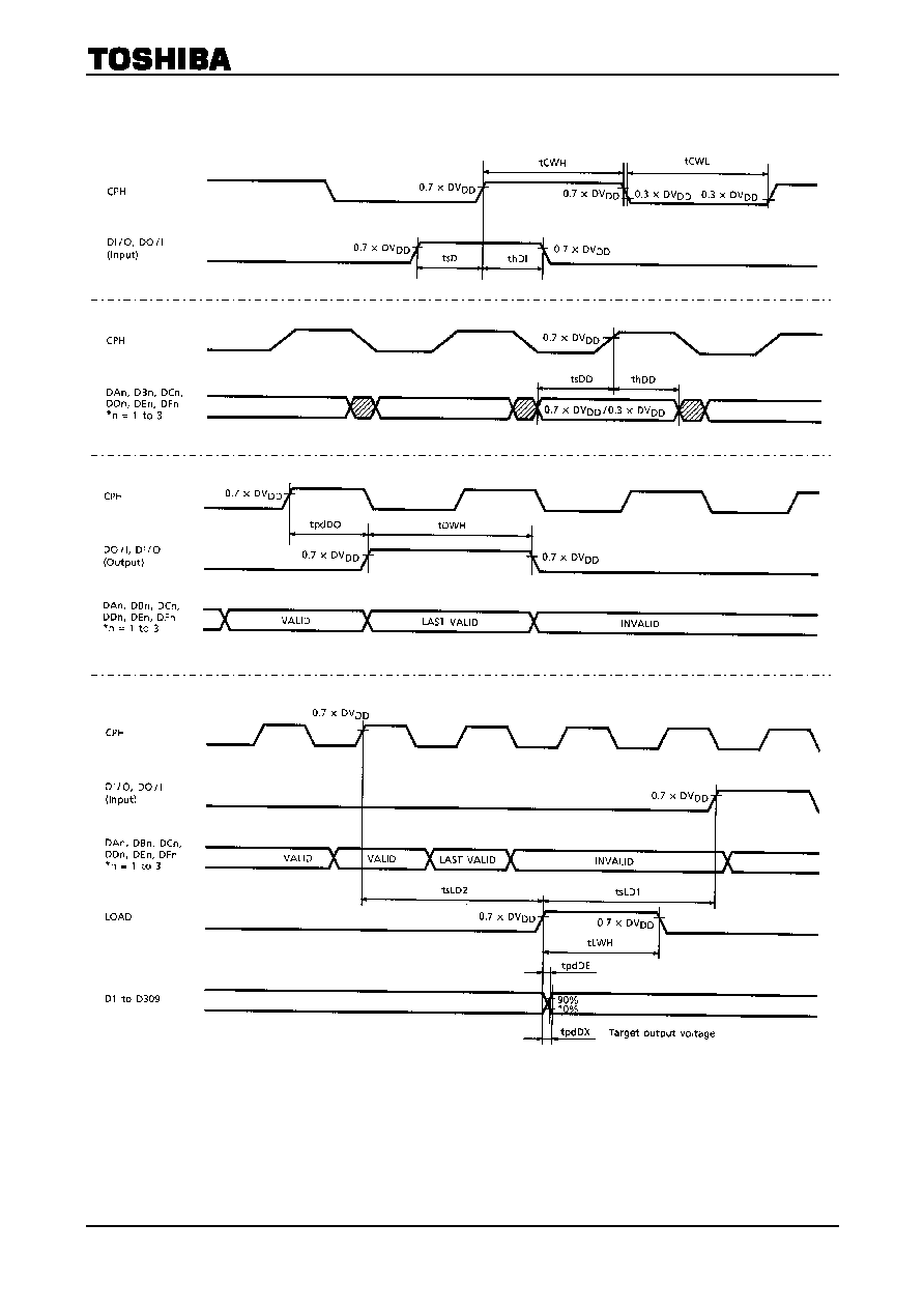
(1) Starting data transfer
A high input to the data transfer enable pin (DI/O or DO/I) is latched into the internal logic synchronously
with the rising edge of CPH, setting the device ready to transfer data. Data transfer starts at the next rise
of CPH (see Fig. 1-1 and 2-1).
This enable pin must not be held for more than one CPH period.
(2) Data transfer method
The data is latched in from the grayscale bus to the sampling register (REG1) synchronously with each
rising edge of CPH.
Grayscale data for three outputs are latched into the device simultaneously in one transfer.
Therefore, the data is latched in 300-output mode by performing 100 transfers, and data is latched in
309-output mode by performing 103 transfers. When the data loading is completed, the device enters a
standby state.
(3) Terminating data transfer
The data transfer enable pin (DO/I or DI/O) output goes high synchronously with the rising edge of CPH one
clock period before the last data is latched in. It is held high until the next rise of CPH (see Fig. 1-1 and
2-1).
The output from this pin can be connected directly as input to the data transfer enable pin (DI/O or DO/I) of
the next stage LCD driver. In this way, multiple devices can be easily cascaded to drive a large screen.
(4) Panel drive output
When a high voltage supplies to the load input, the data in the sampling register (REG1) is transferred to
the load register (REG2) and the device starts updating output to the LCD panel drive pins.
CPH must be held at the DC level for the duration from three CPH periods after a high input to LOAD is
latched in until one clock period before CPH goes high after a high on the data transfer enable pin is latched
in following a 1H period (see Fig. 1-2).

T6L37A
2002-01-07
6
(5) Reference power supply circuit
The connection between the device and the external reference power supply for Reference analog supply is
configured with 7 or 8 resistors of the same specification in series (total of 64 resistor ladders).

T6L37A
2002-01-07
7
(6) Grayscale data and output voltages
The LCD drive output voltages are determined by the grayscale values and the 11 reverence analog inputs
line voltages (V0 to V10).
The three high-order data bits select a pair of reference analog voltages. Calculation of the output voltage
involves multiplying a value derived from the selected reference analog values by a factor determined by the
values of the three low-order bits and dividing by either seven or eight.
Three high-order data bits
DF
n
DE
n
DD
n
Selected
Reference
Voltages
0
0
0
V0 or V1 and V2
0 0 1
V2
and
V3
0 1 0
V3
and
V4
0 1 1
V4
and
V5
1 0 0
V5
and
V6
1 0 1
V6
and
V7
1 1 0
V7
and
V8
1
1
1
V8 and V9 or V10
Three low-order data bits

T6L37A
2002-01-07
8
Grayscale data and output voltages
Note: n
= 1 to 3
Gray-
scale
Data
DFn DEn DDn DCn
DBn DAn
Output
Voltage
Gray-
scale
Data
DFn
DEn
DDn
DCn
DBn DAn
Output
Voltage
00H 0 0 0 0 0 0
V0
20H 1 0 0 0 0 0
V6
+ (V5 - V6) ¥ 7/8
01H 0 0 0 0 0 1
V2
+ (V1 - V2) ¥ 6/7
21H 1 0 0 0 0 1
V6
+ (V5 - V6) ¥ 6/8
02H 0 0 0 0 1 0
V2
+ (V1 - V2) ¥ 5/7
22H 1 0 0 0 1 0
V6
+ (V5 - V6) ¥ 5/8
03H 0 0 0 0 1 1
V2
+ (V1 - V2) ¥ 4/7
23H 1 0 0 0 1 1
V6
+ (V5 - V6) ¥ 4/8
04H 0 0 0 1 0 0
V2
+ (V1 - V2) ¥ 3/7
24H 1 0 0 1 0 0
V6
+ (V5 - V6) ¥ 3/8
05H 0 0 0 1 0 1
V2
+ (V1 - V2) ¥ 2/7
25H 1 0 0 1 0 1
V6
+ (V5 - V6) ¥ 2/8
06H 0 0 0 1 1 0
V2
+ (V1 - V2) ¥ 1/7
26H 1 0 0 1 1 0
V6
+ (V5 - V6) ¥ 1/8
07H 0 0 0 1 1 1
V2
27H 1 0 0 1 1 1
V6
08H 0 0 1 0 0 0
V3
+ (V2 - V3) ¥ 7/8
28H 1 0 1 0 0 0
V7
+ (V6 - V7) ¥ 7/8
09H 0 0 1 0 0 1
V3
+ (V2 - V3) ¥ 6/8
29H 1 0 1 0 0 1
V7
+ (V6 - V7) ¥ 6/8
0AH 0 0 1 0 1 0
V3
+ (V2 - V3) ¥ 5/8
2AH 1 0 1 0 1 0
V7
+ (V6 - V7) ¥ 5/8
0BH 0 0 1 0 1 1
V3
+ (V2 - V3) ¥ 4/8
2BH 1 0 1 0 1 1
V7
+ (V6 - V7) ¥ 4/8
0CH 0 0 1 1 0 0
V3
+ (V2 - V3) ¥ 3/8
2CH 1 0 1 1 0 0
V7
+ (V6 - V7) ¥ 3/8
0DH 0 0 1 1 0 1
V3
+ (V2 - V3) ¥ 2/8
2DH 1 0 1 1 0 1
V7
+ (V6 - V7) ¥ 2/8
0EH 0 0 1 1 1 0
V3
+ (V2 - V3) ¥ 1/8
2EH 1 0 1 1 1 0
V7
+ (V6 - V7) ¥ 1/8
0FH 0 0 1 1 1 1
V3
2FH 1 0 1 1 1 1
V7
10H 0 1 0 0 0 0
V4
+ (V3 - V4) ¥ 7/8
30H 1 1 0 0 0 0
V8
+ (V7 - V8) ¥ 7/8
11H 0 1 0 0 0 1
V4
+ (V3 - V4) ¥ 6/8
31H 1 1 0 0 0 1
V8
+ (V7 - V8) ¥ 6/8
12H 0 1 0 0 1 0
V4
+ (V3 - V4) ¥ 5/8
32H 1 1 0 0 1 0
V8
+ (V7 - V8) ¥ 5/8
13H 0 1 0 0 1 1
V4
+ (V3 - V4) ¥ 4/8
33H 1 1 0 0 1 1
V8
+ (V7 - V8) ¥ 4/8
14H 0 1 0 1 0 0
V4
+ (V3 - V4) ¥ 3/8
34H 1 1 0 1 0 0
V8
+ (V7 - V8) ¥ 3/8
15H 0 1 0 1 0 1
V4
+ (V3 - V4) ¥ 2/8
35H 1 1 0 1 0 1
V8
+ (V7 - V8) ¥ 2/8
16H 0 1 0 1 1 0
V4
+ (V3 - V4) ¥ 1/8
36H 1 1 0 1 1 0
V8
+ (V7 - V8) ¥ 1/8
17H 0 1 0 1 1 1
V4
37H 1 1 0 1 1 1
V8
18H 0 1 1 0 0 0
V5
+ (V4 - V5) ¥ 7/8
38H 1 1 1 0 0 0
V9
+ (V8 - V9) ¥ 6/7
19H 0 1 1 0 0 1
V5
+ (V4 - V5) ¥ 6/8
39H 1 1 1 0 0 1
V9
+ (V8 - V9) ¥ 5/7
1AH 0 1 1 0 1 0
V5
+ (V4 - V5) ¥ 5/8
3AH 1 1 1 0 1 0
V9
+ (V8 - V9) ¥ 4/7
1BH 0 1 1 0 1 1
V5
+ (V4 - V5) ¥ 4/8
3BH 1 1 1 0 1 1
V9
+ (V8 - V9) ¥ 3/7
1CH 0 1 1 1 0 0
V5
+ (V4 - V5) ¥ 3/8
3CH 1 1 1 1 0 0
V9
+ (V8 - V9) ¥ 2/7
1DH 0 1 1 1 0 1
V5
+ (V4 - V5) ¥ 2/8
3DH 1 1 1 1 0 1
V9
+ (V8 - V9) ¥ 1/7
1EH 0 1 1 1 1 0
V5
+ (V4 - V5) ¥ 1/8
3EH 1 1 1 1 1 0
V9
1FH 0 1 1 1 1 1
V5
3FH 1 1 1 1 1 1
V10
Reference analog resistance rate
(R
0
=
=
=
= 2.31 kW
W
W
W)
R
0
R
1
R
2
R
3
R
4
R
5
R
6
R
7
R
8
R
9
1.00 2.00 2.77 1.50 0.90 0.84 0.66 0.84 1.42 1.05

T6L37A
2002-01-07
9
Timing Diagrams
In 300-output mode
Fig. 1-1
Fig. 1-2
Note: Except for D151 to D159

T6L37A
2002-01-07
10
In 309 output mode
Fig. 2-1
Fig. 2-2

T6L37A
2002-01-07
11
Absolute Maximum Ratings
(AV
SS
=
=
=
= DV
SS
=
=
=
= 0 V)
Characteristics Symbol
Rating
Unit
Relevant
Pin
Analog Supply Voltage
AV
DD
-0.3 to 6.5
V
æ
Digital Supply Voltage
DV
DD
-0.3 to AV
DD
+ 0.3
V
æ
Input Voltage
V
IN
-0.3 to DV
DD
+ 0.3
V
æ
Reference Analog Voltage
V (0: 10)
-0.3 to AV
DD
+ 0.3
V
V0 to V10
Storage Temperature
T
stg
-55 to 125
∞C
æ
Recommended Operating Conditions
(AV
SS
=
=
=
= DV
SS
=
=
=
= 0 V)
Characteristics Symbol
Test
Condition Rating
Unit
Relevant
Pin
Analog Supply Voltage
AV
DD
æ
4.5 to 5.5
V
Digital Supply Voltage
DV
DD
æ
3.0 to 3.6
V
Reference Analog Voltage-1
(Note
1)
V1 to V9
æ
AV
SS
+ 0.1 to
AV
DD
- 0.1
V
Case 1
V1 to AV
DD
V0
Case 2
AV
SS
to V1
Case 1
AV
SS
to V9
Reference Analog Voltage-2
(Note
1)
V10
Case 2
V9 to AV
DD
V
Driver Unit Output Voltage
V
OUT
æ
AV
SS
+ 0.1 to
AV
DD
- 0.1
V D1
to
D309
Operating Temperature
T
opr
æ
-20 to 75
∞C
Operating Frequency
f
CPH
æ
DC to 55
MHz
CPH
Output Load Capacitance
C
L
æ
150 (max)
pF /
PIN
D1 to D309
Note 1: The following shows the relative magnitude of each reference analog voltage:
For
case
1
AV
SS
< V10, Vd £ Vd - 1, V0 < AV
DD
(where d
= 9 to 1)
For
case
2
AV
SS
< V0, Vd £ Vd + 1, V10 < AV
DD
(where d
= 1 to 9)

T6L37A
2002-01-07
12
Electrical Characteristics
DC Characteristics
(AV
DD
=
=
=
= 4.5 to 5.5 V, DV
DD
=
=
=
= 3.0 to 3.6 V, AV
SS
=
=
=
= DV
SS
=
=
=
= 0 V, Ta ==== ----20 to 75∞C)
Characteristics Symbol
Test
Circuit
Test Condition
Min
Typ.
Max
Unit
Relevant Pin
Low Level
V
IL
æ
0
æ
0.3
¥
DV
DD
Input Voltage
High Level
V
IH
æ
æ
0.7
¥
DV
DD
æ DV
DD
V Logic
input
Low Level
V
OL
I
OL
= 1.0 mA
DV
SS
æ
DV
SS
+ 0.5
Output Voltage
High Level
V
OH
æ
I
OH
= -1.0 mA
DV
DD
- 0.5
æ
DV
DD
V Logic
output
Ichg
æ
æ
-0.15
Output Current
(Note
2)
Idis
æ
V
OUT
= 0 V
AV
DD
= 5 V
V
X
= 1 V
0.5
æ
æ
mA
D1 to D309
Resistance between
Reference Analog
Voltage Pins
R
GMA
æ
æ
æ 30 æ
k
W V0
to
V10
Output Voltage Deviation
V
DO
æ
æ
æ
±20
æ
mV
D1 to D309
Leakage Current
I
IN
æ
æ
-1.0
æ 1.0 mA Logic
input
Standby Current
ID
STB
æ
fCPH
= DC
-5.0
0.0 5.0
mA DV
DD
AI
DD
æ
fCPH
= 30 MHz
1H
= 30 ms,
no load
Checkerboard pattern
AV
DD
= 5.5 V
æ
4.0 7.0
AV
DD
Current Consumption (1)
DI
DD
æ
fCPH
= 30 MHz
1H
= 30 ms,
no load
Checkerboard pattern
DV
DD
= 3.6 V
æ
6.0 8.0
mA
DV
DD
AI
DD
æ
fCPH
= 20 MHz
1H
= 26.4 ms,
no load
Checkerboard pattern
AV
DD
= 5.0 V
æ
3.5 6.0
AV
DD
Current Consumption (2)
DI
DD
æ
fCPH
= 20 MHz
1H
= 26.4 ms,
no load
Checkerboard pattern
DV
DD
= 3.0 V
æ
2.5 5.5
mA
DV
DD
Note 2: V
X
denotes the voltage applied to the LCD panel drive pin.

T6L37A
2002-01-07
13
AC Characteristics
(AV
DD
=
=
=
= 4.5 to 5.5 V, DV
DD
=
=
=
= 3.0 to 3.6 V, DV
SS
=
=
=
= AV
SS
=
=
=
= 0 V, Ta ==== ----20 to 75∞C)
Characteristics Symbol
Test
Circuit
Test Condition
Min
Typ.
Max
Unit
CPH Pulse Width H
tCWH
æ
æ
4.0
æ
æ
ns
CPH Pulse Width L
tCWL
æ
æ
4.0
æ
æ
ns
Enable Setup Time
tsDI
æ
æ
4.0
æ
æ
ns
Enable Hold Time
thDI
æ
æ
0
æ
æ
ns
Enable Pulse Width H
tDWH
æ
æ
æ 1.0 æ
CPH
period
Data Setup Time
tsDD
æ
æ
4.0
æ
æ
ns
Data Hold Time
thDD
æ
æ
0
æ
æ
ns
Output Delay Time 1
tpdDO
æ
C
L
= 35 pF
æ
æ
14.0
ns
Output Delay Time 2
tpdDE
æ
C
L
= 2 kW + 75 pF ¥ 2
Target output voltage ±
AV
DD
¥
0.1
æ
æ
3.0
ms
Output Delay Time 3
tpdDX
æ
C
L
= 2 KW + 75 pF ¥ 2
Target output voltage
æ
æ
10.0
ms
LOAD Setup Time 1
tsLD1
æ
æ
1.0
æ
æ
CPH
period
LOAD Setup Time 2
tsLD2
æ
æ
7.0
æ
æ
ns
LOAD Pulse Width H
tLWH
æ
æ
2.0
æ
æ
CPH
period
T6L37A
2002-01-07
14

T6L37A
2002-01-07
15
∑ TOSHIBA is continually working to improve the quality and reliability of its products. Nevertheless, semiconductor
devices in general can malfunction or fail due to their inherent electrical sensitivity and vulnerability to physical
stress. It is the responsibility of the buyer, when utilizing TOSHIBA products, to comply with the standards of
safety in making a safe design for the entire system, and to avoid situations in which a malfunction or failure of
such TOSHIBA products could cause loss of human life, bodily injury or damage to property.
In developing your designs, please ensure that TOSHIBA products are used within specified operating ranges as
set forth in the most recent TOSHIBA products specifications. Also, please keep in mind the precautions and
conditions set forth in the "Handling Guide for Semiconductor Devices," or "TOSHIBA Semiconductor Reliability
Handbook" etc..
∑ The TOSHIBA products listed in this document are intended for usage in general electronics applications
(computer, personal equipment, office equipment, measuring equipment, industrial robotics, domestic appliances,
etc.). These TOSHIBA products are neither intended nor warranted for usage in equipment that requires
extraordinarily high quality and/or reliability or a malfunction or failure of which may cause loss of human life or
bodily injury ("Unintended Usage"). Unintended Usage include atomic energy control instruments, airplane or
spaceship instruments, transportation instruments, traffic signal instruments, combustion control instruments,
medical instruments, all types of safety devices, etc.. Unintended Usage of TOSHIBA products listed in this
document shall be made at the customer's own risk.
∑ Polyimide base film is hard and thin. Be careful not to injure yourself on the film or to scratch any other parts with
the film. Try to design and manufacture products so that there is no chance of users touching the film after
assembly, or if they do , that there is no chance of them injuring themselves. When cutting out the film, try to
ensure that the film shavings do not cause accidents. After use, treat the leftover film and reel spacers as
industrial waste.
∑ Light striking a semiconductor device generates electromotive force due to photoelectric effects. In some cases
this can cause the device to malfunction.
This is especially true for devices in which the surface (back), or side of the chip is exposed. When designing
circuits, make sure that devices are protected against incident light from external sources. Exposure to light both
during regular operation and during inspection must be taken into account.
∑ The products described in this document are subject to the foreign exchange and foreign trade laws.
∑ The information contained herein is presented only as a guide for the applications of our products. No
responsibility is assumed by TOSHIBA CORPORATION for any infringements of intellectual property or other
rights of the third parties which may result from its use. No license is granted by implication or otherwise under
any intellectual property or other rights of TOSHIBA CORPORATION or others.
∑ The information contained herein is subject to change without notice.
000707EBE
RESTRICTIONS ON PRODUCT USE