 | –≠–ª–µ–∫—Ç—Ä–æ–Ω–Ω—ã–π –∫–æ–º–ø–æ–Ω–µ–Ω—Ç: TA1287PG | –°–∫–∞—á–∞—Ç—å:  PDF PDF  ZIP ZIP |

TA1287PG,TA1287FG
2004-08-03
1
TOSHIBA BIPOLAR LINEAR INTEGRATED CIRCUIT SILICON MONOLITHIC
TA1287PG,TA1287FG
RGB TO YUV / IQ HIGH-SPEED MATRIX IC
TA1287PG, TA1287FG are a high-speed switching IC which have
2-channel inputs circuit and a RGB to YUV / IQ matrix circuit.
Another feature, TA1287PG, TA1287FG have a signals mixing
circuit, which are enable to mix a main signal with an external
input signal and outputs the mixed signal. The mixing circuit has
8 combinations of mixing gain ratio of a main to an external
signals, which is controlled by high-speed switch.
FEATURES
RGB to YUV / IQ matrix circuit
The mixing circuit for a main signal and an external signal
The high-speed switching circuit of a main signal an external
signal
Band Width : 30MHz at -3dB point.
TA1287PG
TA1287FG
Weight
DIP16-P-300-2.54A: 1.0 g (typ.)
SSOP16-P-225-1.00A: 0.14 g (typ.)

TA1287PG,TA1287FG
2004-08-03
2
BLOCK DIAGRAM

TA1287PG,TA1287FG
2004-08-03
3
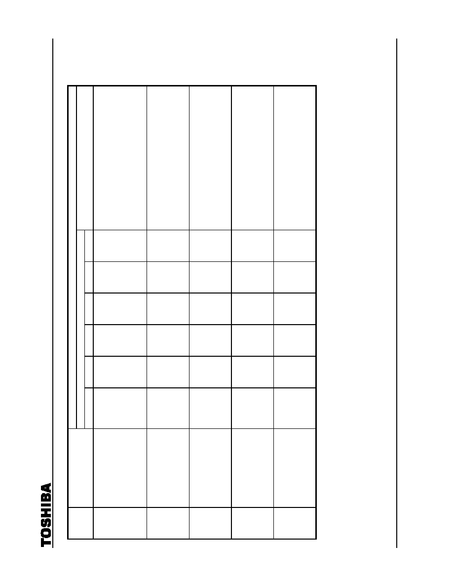
TERMINAL FUNCTIONS
PIN
No.
PIN
NAME
FUNCTION INTERFACE
CIRCUIT
INPUT / OUTPUT
SIGNAL
1 V
IN
Input R-Y (V) or R signal
through a clamping
capacitor.
2 Y
IN
Input Y or G signal
through a clamping
capacitor.
3 U
IN
Input B-Y (U) or B signal
through a clamping
capacitor.
DC :
6.2
V
Y : 1 V
p-p
(with sync)
U / V : 0.3 V
p-p
(B : C = 1 : 1)
R / G / B
:
0.7
V
p-p
(100%
white)
4 CP
IN
Input clamping pulse.
Threshold : 0.75 V
5
GND
GND.
6 R
IN
Input R or R-Y (V) signal
through clamping
capacitor.
7 G
IN
Input G or Y signal
through a clamping
capacitor.
8 B
IN
Input B or B-Y (U) signal
through a clamping
capacitor.
DC : 6.2 V
Y
: 1V
p-p
(with sync)
U / V : 0.3 V
p-p
(B : C = 1 : 1)
R / G / B
:
0.7
V
p-p
(100%
white)
TA1287PG,TA1287FG
2004-08-03
4
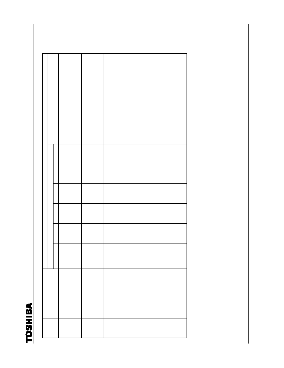
PIN
No
PIN
NAME
FUNCTION INTERFACE
CIRCUIT
INPUT / OUTPUT
SIGNAL
9
10
11
YS1,2, 3
Selector to switch mixing
ratios.
Threshold : 0.75 V
12 V
CC
Supply 9 V.
DC : 9 V
13 V
OUT
Outputs R-Y (V) or R
signal.
14 Y
OUT
Outputs Y or G signal.
15
U
OUT
Outputs B-Y (U) or B
signal.
DC : 4.7
V
Y :
1
V
p-p
(with sync)
U / V : 0.3 V
p-p
(B : C = 1 : 1)
R / G / B
:
0.7
V
p-p
(100% color bar)
16
Matrix
Control
This terminal's voltage
control the matrix
coefficient for output
signals.Selects the output
mode.

TA1287PG,TA1287FG
2004-08-03
5
FUNCTION DESCRIPTION
MIXING RATIO
TA1287PG, TA1287FG have a circuit, which mixes a main signal with an external input signal and outputs
the mixed signal. The mixing circuit has 8 combinations of mixing gain ratio of a main to an external
signals.
Table The mixing ratio of external to main (TV)
THE MIXING RATIO
YS1 YS2 YS3
EXTERNAL MAIN
(TV)
L L L
0
1
H L L
0.3
0.7
L H L
0.4
0.6
H H L
0.5
0.5
L L H
0.6
0.4
H L H
0.7
0.3
L H H
0.8
0.2
H H H
1
0
MATRIX CONTROL
Pin 16 is a high-speed switch to control the matrix mode for output signals.
Table Matrix mode depending on by the voltage of pin 16
VOLTAGE OF PIN 16 [V]
MODE
0 ~ 0.7
Through
~
2.3
RGB to YUV (PAL)
~
3.8
RGB to YUV (NTSC)
3.8 ~
RGB to YIQ

TA1287PG,TA1287FG
2004-08-03
6
MAXIMUM RATINGS
(Ta = 25∞C)
CHARACTERISTIC
SYMBOL RATING UNIT
Supply Voltage
V
CCmax
12 V
Input Pin Voltage
V
in
GND
- 0.3 to V
CC
+ 0.3
V
TA1287PG
P
DD
(Note 1)
1400
Power Consumption
TA1287FG
P
DF
(Note 1)
641
mW
TA1287PG 1
/
jaD
-11.2 mW
/
∞C
Power
Consumption
Reduction Ratio
TA1287FG 1
/
jaF
-5.13 mW
/
∞C
Operating Temperature
T
opr
-20~65 ∞C
Storage Temperature
T
stg
-55~150 ∞C
Note 1: Refer to the figure below.
Note 2: It is possible that TA1287FG function faultily caused by leak problems according to a field intensity from CRT.
Put IC lay-out position to CRT be far more than 20 cm. If there is not a enough distance, intercept it by a
shield.
Fig. Power consumption reduction against ambient temperature

TA1287PG,TA1287FG
2004-08-03
7
OPERATING CONDITIONS
CHARACTERISTIC DESCRIPTION
MIN
TYP.
MAX
UNIT
Supply Voltage
Pin 12
8.1
9.0
9.9
V
Y Input Signal Level
White : 100% with sync.
1.0
V
p-p
U Input Signal Level
B : C = 1 : 1
300 mV
p-p
V Input Signal Level
B : C = 1 : 1
300 mV
p-p
R Input Signal Level
100% white
700 mV
p-p
G Input Signal Level
100% white
700 mV
p-p
B Input Signal Level
100% white
700 mV
p-p
CP Input Level
Pin 4
1.1
1.5
5.0
V
YS1, YS2, YS3, Input Level
Pin 9, 10, 11
1.1
1.5
5.0
V
ELECTRICAL CHARACTERISTICS
(V
CC
= 9V and Ta = 25∞C, unless otherwise specified)
Current consumption
PIN NAME
SYMBOL
TESTCIRCUIT
MIN
TYP.
MAX
UNIT
V
CC
I
CC
20.0
26.0
32.0
mA
Terminal voltages
PIN No.
PIN NAME
SYMBOL
TEST CIRCUIT
MIN
TYP.
MAX
UNIT
1 V
IN
V
1
6.0 6.2 6.4
2 Y
IN
V
2
6.0 6.2 6.4
3 U
IN
V
3
6.0 6.2 6.4
6 R
IN
V
6
6.0 6.2 6.4
7 G
IN
V
7
6.0 6.2 6.4
8 B
IN
V
8
6.0 6.2 6.4
13 V
OUT
V
13
4.5 4.7 4.9
14 Y
OUT
V
14
4.5 4.7 4.9
15 U
OUT
V
15
4.5 4.7 4.9
V
TA1287PG,TA1287FG
2004-08-03
8
AC CHARACTERISTICS
CHARACTERISTIC SYMBOL
TEST
CIR-
CUIT
TEST CONDITION
MIN
TYP.
MAX
UNIT
YUV Gain
(Through Mode)
GTRY
GTY
GTBY
(Note
A
1
)
-0.5
-0.5
-0.5
0
0
0
0.5
0.5
0.5
dB
RGB Gain
(Through Mode)
GRR
GRG
GRB
(Note
A
2)
-0.5
-0.5
-0.
5
0
0
0
0.5
0.5
0.5
dB
R Gain (Input to Pin 6)
(Matrix Mode)
GRRYP
GRYP
GRBYP
GRRYN
GRYN
GRBYN
GRRYI
GRYI
GRBYI
(Note
A
3
)
-4.7
-10.3
-17.3
-4.3
-10.3
-18.4
-4.6
-10.3
-13.0
-4.2
-9.8
-16.8
-3.8
-9.8
-17.9
-4.1
-9.8
-12.5
-3.7
-9.3
-16.3
-3.3
-9.3
-17.4
-3.6
-9.6
-12.0
dB
G Gain (Input to Pin 7)
(Matrix Mode)
GGRYP
GGYP
GGBYP
GGRYN
GGYN
GGBYN
GGRYI
GGYI
GGBYI
(Note
A
4
)
-6.3
-4.5
-11.5
-5.9
-4.5
-10.9
-11.5
-4.5
-5.6
-5.8
-4.0
-11.0
-5.4
-4.0
-10.4
-11.0
-4.0
-5.1
-5.3
-3.5
-10.5
-4.9
-3.5
-9.9
-10.5
-3.5
-4.6
dB
B Gain (Input to Pin 8)
(Matrix Mode)
GBRYP
GBYP
GBBYP
GBRYN
GBYN
GBBYN
GBRYI
GBYI
GBBYI
(Note
A
5
) -21.1
-19.1
-7.7
-20.3
-19.1
-7.9
-10.2
-19.1
-10.7
-20.6
-18.6
-7.2
-19.8
-18.6
-7.4
-9.7
-18.6
-10.2
-20.1
-18.1
-6.7
-19.3
-18.1
-6.9
-9.2
-18.1
-9.7
dB
R-Y Gain (Input to Pin 1)
(Matrix Mode)
GTRY73
GTRY64
GTRY55
GTRY46
GTRY37
GTRY28
(Note
A
6
)
-3.7
-5.0
-6.6
-8.5
-11.0
-14.3
-3.2
-4.5
-6.1
-8.0
-10.5
-13.8
-2.7
-4.0
-5.6
-7.5
-10.0
-13.3
dB

TA1287PG,TA1287FG
2004-08-03
9
CHARACTERISTIC SYMBOL
TEST
CIR-
CUIT
TEST CONDITION
MIN
TYP.
MAX
UNIT
Y Gain (Input to Pin 2)
(Mixing Mode)
GTY73
GTY64
GTY55
GTY46
GTY37
GTY28
(Note
A
7
)
-3.7
-5.0
-6.6
-8.5
-11.0
-14.3
-3.2
-4.5
-6.1
-8.0
-10.5
-13.8
-2.7
-4.0
-5.6
-7.5
-10.0
-13.3
dB
B-Y Gain (Input to Pin 3)
(Mixing Mode)
GTBY73
GTBY64
GTBY55
GTBY46
GTBY37
GTBY28
(Note
A
8
)
-3.7
-5.0
-6.6
-8.5
-11.0
-14.3
-3.2
-4.5
-6.1
-8.0
-10.5
-13.8
-2.7
-4.0
-5.6
-7.5
-10.0
-13.3
dB
R Gain (Input to Pin 6)
(Mixing Mode)
GRR37
GRR46
GRR55
GRR64
GRR73
GRR82
(Note
A
9
)
-3.7
-5.0
-6.6
-8.5
-11.0
-14.3
-3.2
-4.5
-6.1
-8.0
-10.5
-13.8
-2.7
-4.0
-5.6
-7.5
-10.0
-13.3
dB
G Gain (Input to Pin 7)
(Mixing Mode)
GRG37
GRG46
GRG55
GRG64
GRG73
GRG82
(Note
A
10
)
-3.7
-5.0
-6.6
-8.5
-11.0
-14.3
-3.2
-4.5
-6.1
-8.0
-10.5
-13.8
-2.7
-4.0
-5.6
-7.5
-10.0
-13.3
dB
B Gain (Input to Pin 8)
(Mixing Mode)
GRB37
GRB46
GRB55
GRB64
GRB73
GRB82
(Note
A
11
)
-3.7
-5.0
-6.6
-8.5
-11.0
-14.3
-3.2
-4.5
-6.1
-8.0
-10.5
-13.8
-2.7
-4.0
-5.6
-7.5
-10.0
-13.3
dB
YUV Input Dynamic Range
(Through Mode)
DTV
DTY
DTU
(Note
A
12
)
1.2
1.2
1.2
1.5
1.5
1.5
1.7
1.7
1.7
V
p-p
RGB Input Dynamic Range
(Through Mode)
DRR
DRG
DRB
(Note
A
13
)
1.2
1.2
1.2
1.5
1.5
1.5
1.7
1.7
1.7
V
p-p
R Input Dynamic Range
(Input to Pin 6)
(Matrix Mode)
DRP
DRNU
DRNI
(Note
A
14
)
1.2
1.2
1.2
1.5
1.5
1.5
1.7
1.7
1.7
V
p-p
G Input Dynamic Range
(Input to Pin 7)
(Matrix Mode)
DGP
DGNU
DGNI
(Note
A
15
)
1.2
1.2
1.2
1.5
1.5
1.5
1.7
1.7
1.7
V
p-p

TA1287PG,TA1287FG
2004-08-03
10
CHARACTERISTIC SYMBOL
TEST
CIR-
CUIT
TEST CONDITION
MIN
TYP.
MAX
UNIT
B Input Dynamic Range
(Input to Pin 8)
(Matrix Mode)
DBP
DBNU
DBNI
(Note
A
16
)
1.2
1.2
1.2
1.5
1.5
1.5
1.7
1.7
1.7
V
p-p
YUV Input and Output
Frequency Characteristic
(At -3 dB Point)
(Through Mode)
GfTRY
GfTY
GfTBY
(Note
A
17
)
30
30
30
MHz
RGB Input and Output
Frequency Characteristic
(At -3 dB Point)
(Through Mode)
GfRR
GfRG
GfRB
(Note
A
18
)
30
30
30
MHz
Ys Switching Delay
Time
YsRYR
YsRRY
YsYG
YsGY
YsBYB
YsBBY
(Note
A
19
)
25.0
20.0
25.0
20.0
25.0
20.0
40.0
40.0
40.0
40.0
40.0
40.0
ns
Crosstalk between Each
Input
(Note
A
20
)
-50
-40 dB

TA1287PG,TA1287FG
2004-08-03
11
TEST CONDITION
TEST CONDITION (UNLESS OTHERWISE SPECIFIED, V
CC
= 9 V and Ta = 25 ± 3∞C)
SW MODE
NOTE ITEM
SW
9
SW
10
SW
11
SW
16A
SW
16B
SW
16C
MEASURING METHOD
<Common
test
condition>
1) V
CC
= 9 V and Ta = 25 ± 3∞C.
2) ALL switch modes are B, unless otherwise
specified.
A
1
YUV
Gain
(Through Mode)
B
B
B
B
B
B
1) Input Signal 1 into pin 4
2) Supply DC 0 V to YS1 (pin 9), YS2 (pin 10), YS (pin
11).
3) Input Signal 2 (f
0
= 100 kHz, V
0
= 0.2 Vp-p) into
V-IN (pin 1, SW
1
= A).
4) Measure the amplitude of V-OUT at pin 13.
Calculate the gain. (GTRY)
5) Calculate gains of Y-IN to Y-OUT and U-IN to
U-OUT, in the same way as 3) to 4)
GTY :
Y-IN (pin 2)
to Y-OUT (pin 14)
GTBY :
U-IN (pin 3)
to U-OUT (pin 15)
A
2
RGB
Gain
(Through Mode)
A
A
A
B
B
B
1) Calculate gains against R, G and B, in the same
way as NOTE A
1
.
GRR : SW
6
= A, R-IN (pin 6)
to V-OUT (pin 13)
GRG : SW
7
= A, R-IN (pin 7)
to Y-OUT (pin 14)
GRB : SW
8
= A, R-IN (pin 8)
to U-OUT (pin 15)
TA1287PG,TA1287FG
2004-08-03
12
TEST CONDITION (UNLESS OTHERWISE SPECIFIED, V
CC
= 9 V and Ta = 25 ± 3∞C)
SW MODE
NOTE ITEM
SW
9
SW
10
SW
11
SW
16A
SW
16B
SW
16C
MEASURING METHOD
1) Calculate gains against each item, in the same way
as NOTE A
1
.
A
A
A
B
B
A
(PAL)
GRRYP :
R-IN (pin 6)
to V-OUT (pin 13)
GRYP
:
R-IN (pin 6)
to Y-OUT (pin 14)
GRBYP :
R-IN (pin 6)
to U-OUT (pin 15)
A
B
A
(NTSC,
UV)
GRRYN :
R-IN (pin 6)
to V-OUT (pin 13)
GRYN
:
R-IN (pin 6)
to Y-OUT (pin 14)
GRBYN :
R-IN (pin 6)
to U-OUT (pin 15)
A
3
R
Gain
(Input to Pin 6)
(Matrix Mode)
A A A
(NTSC,
IQ)
GRRYI :
R-IN (pin 6)
to V-OUT (pin 13)
GRYI
:
R-IN (pin 6)
to Y-OUT (pin 14)
GRBYI :
R-IN (pin 6)
to U-OUT (pin 15)
TA1287PG,TA1287FG
2004-08-03
13
TEST CONDITION (UNLESS OTHERWISE SPECIFIED, V
CC
= 9 V and Ta = 25 ± 3∞C)
SW MODE
NOTE ITEM
SW
9
SW
10
SW
11
SW
16A
SW
16B
SW
16C
MEASURING METHOD
1) Calculate gains against each item, in the same way
as NOTE A
1
.
A
A
A
B
B
A
(PAL)
GGRYP :
G-IN (pin 7)
to V-OUT (pin 13)
GGYP :
G-IN (pin 7)
to Y-OUT (pin 14)
GGBYP :
G-IN (pin 7)
to U-OUT (pin 15)
A
B
A
(NTSC,
UV)
GGRYN :
G-IN (pin 7)
to V-OUT (pin 13)
GGYN :
G-IN (pin 7)
to Y-OUT (pin 14)
GGBYN :
G-IN (pin 7)
to U-OUT (pin 15)
A
4
G
Gain
(Input to Pin 7)
(Matrix Mode)
A A A
(NTSC,
IQ)
GGRYI :
G-IN (pin 7)
to V-OUT (pin 13)
GGYI
:
G-IN (pin 7)
to Y-OUT (pin 14)
GGBYI :
G-IN (pin 7)
to U-OUT (pin 15)

TA1287PG,TA1287FG
2004-08-03
14
TEST CONDITION (UNLESS OTHERWISE SPECIFIED, V
CC
= 9 V and Ta = 25 ± 3∞C)
SW MODE
NOTE ITEM
SW
9
SW
10
SW
11
SW
16A
SW
16B
SW
16C
MEASURING METHOD
1) Calculate gains against each item, in the same way
as NOTE A
1
.
A A A B B
B
(PAL)
GGRYP :
B-IN (pin 8)
to V-OUT (pin 13)
GGYP : B-IN (pin 8)
to Y-OUT (pin 14)
GGBYP : B-IN (pin 8)
to U-OUT (pin 15)
A B A
(NTSC,
UV)
GGRYN :
B-IN (pin 8)
to V-OUT (pin 13)
GGYN : B-IN (pin 8)
to Y-OUT (pin 14)
GGBYN : B-IN (pin 8)
to U-OUT (pin 15)
A
5
B
Gain
(Input to Pin 8)
(Matrix Mode)
A A A
(NTSC,
IQ)
GGRYI : B-IN (pin 8)
to V-OUT (pin 13)
GGYI : B-IN (pin 8)
to Y-OUT (pin 14)
GGBYI : B-IN (pin 8)
to U-OUT (pin 15)
TA1287PG,TA1287FG
2004-08-03
15
TEST CONDITION (UNLESS OTHERWISE SPECIFIED, V
CC
= 9 V and Ta = 25 ± 3∞C)
SW MODE
NOTE ITEM
SW
9
SW
10
SW
11
SW
16A
SW
16B
SW
16C
MEASURING METHOD
A
6
R-Y
Gain
(Input to Pin 1)
(Mixing Mode)
A
B
A
B
A
B
B
A
A
B
B
A
B
B
B
A
A
A
B B B
1)
Input
Signal
into
pin
4.
2) Supply DC 0V to YS1 (pin 9), YS2 (pin 10), YS3
(pin 11).
3) Input Signal 2 (f
0
= 100 kHz, V
0
= 0.2 V
p-p
) into
V-IN (pin 1, SW
1
= A).
4) Measure each amplitude of output signal from
V-OUT (pin 13) in each SW MODE. Calculate the
gains.
A
7
Y
Gain
(Input to Pin 2)
(Mixing Mode)
A
B
A
B
A
B
B
A
A
B
B
A
B
B
B
A
A
A
B
B
B
1) Calculate gains of Y-IN (pin 2) to Y-OUT (pin 14), in
the same way as NOTE A
6
. (SW
2
= A)
A
8
B-Y
Gain
(Input to Pin 3)
(Mixing Mode)
A
B
A
B
A
B
B
A
A
B
B
A
B
B
B
A
A
A
B
B
B
1) Calculate gains of U-IN (pin 3) to Y-OUT (pin 15), in
the same way as NOTE A
6
. (SW
3
= A)
A
9
R
Gain
(Input to Pin 6)
(Mixing Mode)
A
B
A
B
A
B
B
A
A
B
B
A
B
B
B
A
A
A
B
B
B
1) Calculate gains of R-IN (pin 6) to V-OUT (pin 13), in
the same way as NOTE A
6
. (SW
6
= A)
A
10
G
Gain
(Input to Pin 7)
(Mixing Mode)
A
B
A
B
A
B
B
A
A
B
B
A
B
B
B
A
A
A
B
B
B
1) Calculate gains of G-IN (pin 7) to Y-OUT (pin 14),
in the same way as NOTE A
6
. (SW
7
= A)

TA1287PG,TA1287FG
2004-08-03
16
TEST CONDITION (UNLESS OTHERWISE SPECIFIED, V
CC
= 9 V and Ta = 25 ± 3∞C)
SW MODE
NOTE ITEM
SW
9
SW
10
SW
11
SW
16A
SW
16B
SW
16C
MEASURING METHOD
A
11
B Gain
(Input to Pin 8)
(Mixing Mode)
A
B
A
B
A
B
B
A
A
B
B
A
B
B
B
A
A
A
B
B
B
1) Calculate gains of B-IN (pin 8) to U-OUT (pin 15), in
the same way as NOTE A
6
. (SW
8
= A)
A
12
YUV Input Dynamic Range
(Through Mode)
B
B
B
B
B
B
1) Input Signal into pin 4.
2) Supply DC 0V to YS1 (pin 9), YS2 (pin 10), YS3
(pin 11).
3) Input Signal 2 (f
0
= 100 kHz, V
0
= 0.2 V
p-p
) into
V-IN (pin 1, SW
1
= A).
4) Increase the amplitude of input-signal 2 gradually.
Measure the biggest amplitude of input-signal 2
without any distortion on V-OUT wave shape.
(DTRY)
5) Measure in the same way as (pin 3) to (pin 4) for
Y-IN (pin 2, SW
2
= A) and U-IN (pin 3, SW
3
= A),
DTY
:
Y-IN (pin 2)
to Y-OUT (pin 14)
DTBY
:
U-IN (pin 3)
to U-OUT (pin 15)
A
13
RGB Input Dynamic Range
(Through Mode)
B
B
B
B
B
B
1) Measure in the same way as NOTE A
12
for R-IN
(pin 6, SW
6
= A) G-IN (pin 7, SW
7
= A) and B-IN
(pin 8, SW
8
= A).
A
14
R Input Dynamic Range
(Input to Pin 6)
(Matrix Mode)
A A A B
A
A
B
B
A
A
A
A
1) For each combination of SW
16A, 16B
and
16C
,
measure each item in the same way as 1) to 4) of
NOTE A
12
.
(SW
6
= A, R-IN (pin 6) to V-OUT (pin 13))
DRP
: PAL
DRNU
:
NTSC,
UV
DRNI : NTSC, IQ
TA1287PG,TA1287FG
2004-08-03
17
TEST CONDITION (UNLESS OTHERWISE SPECIFIED, V
CC
= 9 V and Ta = 25 ± 3∞C)
SW MODE
NOTE ITEM
SW
9
SW
10
SW
11
SW
16A
SW
16B
SW
16C
MEASURING METHOD
A
15
G Input Dynamic Range
(Input to Pin 7)
(Matrix Mode)
A A A B
A
A
B
B
A
A
A
A
1) Measure each item in the same way as NOTE A
14
.
(SW
7
= A, G-IN (pin 7) to Y-OUT (pin 14))
DGP
: PAL
DGNU : NTSC,
UV
DGNI : NTSC, IQ
A
16
B Input Dynamic Range (Input
to Pin 8)
(Matrix Mode)
A A A B
A
A
B
B
A
A
A
A
1) Measure each item in the same way as NOTE A
14
.
(SW
8
= A, B-IN (pin 8) to U-OUT (pin 15))
DBP
:
PAL
DBNU : NTSC, UV
DBNI : NTSC, IQ
A
17
YUV Input and Output
Frequency Characteristic
(At -3 dB Point)
(Through Mode)
B
B
B
B
B
B
1) Input Signal 1 into pin 4.
2) Supply DC 0V to YS1 (pin 9), YS2 (pin 10), YS3
(pin 11).
3) Input Signal 2 (f
0
= 30 MHz, V
0
= 0.2 V
p-p
) into
V-IN (pin 1, SW
1
= A).
4) Measure the amplitude during picture period on
V-OUT (pin13). (v
13
-30 MHz)
5) Calculate the frequency gain by using the following
equation and v
13
, which is measured as the output
amplitude in NOTE A
1
.
GfTRY = 20 og
l
(v
13
-30 MHz / v
13
)
6) Calculate following items, in the same way as
clause 5).
GfTY
: Y-IN (pin 2)
to Y-OUT (pin 14)
GfTBY : U-IN (pin 3)
to U-OUT (pin 15)
TA1287PG,TA1287FG
2004-08-03
18
TEST CONDITION (UNLESS OTHERWISE SPECIFIED, V
CC
= 9 V and Ta = 25 ± 3∞C)
SW MODE
NOTE ITEM
SW
9
SW
10
SW
11
SW
16A
SW
16B
SW
16C
MEASURING METHOD
A
18
RGB Input and Output
Frequency Characteristic
(At -3 dB Point)
(Through Mode)
A
A
A
B
B
B
1) In the same way as NOTE A
17
, calculate items
against R-IN (pin 6, SW
6
= A), G-IN (pin 7, SW
7
=
A) and B-IN (pin 8, SW
8
= A).
GfRR
:
R-IN (pin 6)
to V-OUT (pin 13)
GfRG : G-IN (pin 7)
to Y-OUT (pin 14)
GfRB : B-IN (pin 8)
to U-OUT (pin 15)
A
19
Ys Switching Delay Time
B
B
B
1) Input Signal 1 into pin 4.
2) Input Signal 3 into R-IN (pin 6, SW
6
= A). Input
Signal 4 into YS1 (pin 9), YS2 (pin 10), YS3 (pin
11).
3) Measure (I) and (II) periods on V-OUT (pin 13).
4) Measure in the same way as 2) to 3) for G-IN (pin 7,
SW
7
= A) and B-IN (pin 8, SW
8
= A).
R-IN
(I) : YsRYR
(II) : YsRYR
G-IN
(I) : YsYG
(II) : YsYG
B-IN
(I) : YsBYB
(II) : YsBBY
A
20
Crosstalk between Each Input
A
or
B
A
or
B
A
or
B
B
B
B
1) Input Signal into pin 4.
2) Supply DC 0V to YS1 (pin 9), YS2 (pin 10), YS3
(pin 11).
3) Input Signal 2 (f
0
= 4 MHz, V
0
= 0.5 V
p-p
) into V-IN
(pin 1, SW
1
= A).
4) Changing
SW
9
, SW
10
, and SW
11
against each
case, measure each leak levels.
5) Calculate the gains, input level to leak level.
TA1287PG,TA1287FG
2004-08-03
19
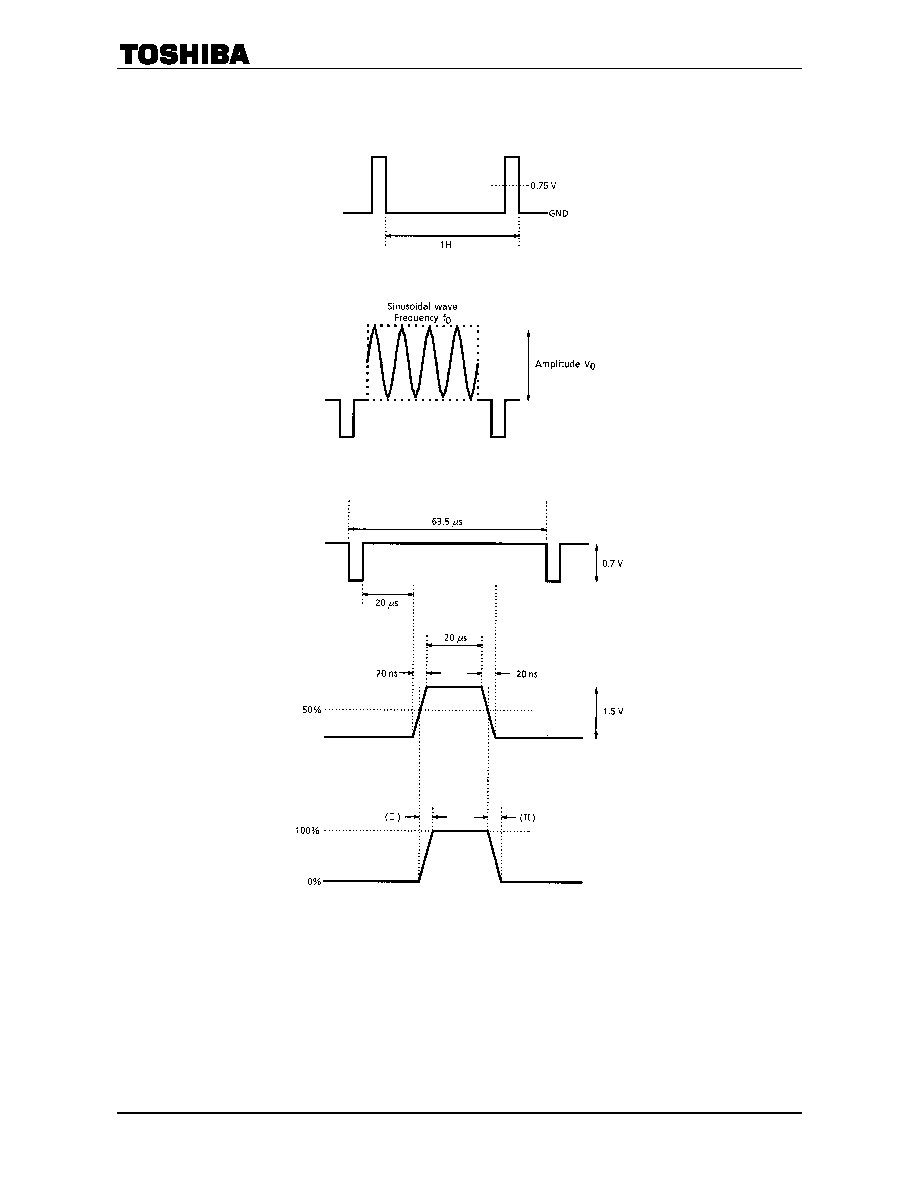
TEST SIGNALS
Signal 1
Signal 2
Signal 3
Signal 4
Output wave-form

TA1287PG,TA1287FG
2004-08-03
20
TEST CIRCUIT

TA1287PG,TA1287FG
2004-08-03
21
APPLICATION CIRCUIT
THE MIXING RATIO TABLE FOR EXTERNAL TO TV
Ys1
Ys2
Ys3
EXT : TV
L
L
L
0 : 1
H
L
L
0.3 : 0.7
L H L
0.4
:
0.6
H
H
L
0.5 : 0.5
L
L
H
0.6 : 0.4
H
L
H
0.7 : 0.3
L
H
H
0.8 : 0.2
H H H
1
:
0

TA1287PG,TA1287FG
2004-08-03
22
PACKAGE DIMENSIONS
Weight: 1.0g (Typ.)

TA1287PG,TA1287FG
2004-08-03
23
PACKAGE DIMENSIONS
Weight: 0.14g (Typ.)

TA1287PG,TA1287FG
2004-08-03
24
∑ The information contained herein is subject to change without notice.
∑ The information contained herein is presented only as a guide for the applications of our products. No
responsibility is assumed by TOSHIBA for any infringements of patents or other rights of the third parties which
may result from its use. No license is granted by implication or otherwise under any patent or patent rights of
TOSHIBA or others.
∑ TOSHIBA is continually working to improve the quality and reliability of its products. Nevertheless, semiconductor
devices in general can malfunction or fail due to their inherent electrical sensitivity and vulnerability to physical
stress. It is the responsibility of the buyer, when utilizing TOSHIBA products, to comply with the standards of
safety in making a safe design for the entire system, and to avoid situations in which a malfunction or failure of
such TOSHIBA products could cause loss of human life, bodily injury or damage to property.
In developing your designs, please ensure that TOSHIBA products are used within specified operating ranges as
set forth in the most recent TOSHIBA products specifications. Also, please keep in mind the precautions and
conditions set forth in the "Handling Guide for Semiconductor Devices," or "TOSHIBA Semiconductor Reliability
Handbook" etc..
∑ The TOSHIBA products listed in this document are intended for usage in general electronics applications
(computer, personal equipment, office equipment, measuring equipment, industrial robotics, domestic appliances,
etc.). These TOSHIBA products are neither intended nor warranted for usage in equipment that requires
extraordinarily high quality and/or reliability or a malfunction or failure of which may cause loss of human life or
bodily injury ("Unintended Usage"). Unintended Usage include atomic energy control instruments, airplane or
spaceship instruments, transportation instruments, traffic signal instruments, combustion control instruments,
medical instruments, all types of safety devices, etc.. Unintended Usage of TOSHIBA products listed in this
document shall be made at the customer's own risk.
∑ The products described in this document are subject to the foreign exchange and foreign trade laws.
∑ TOSHIBA products should not be embedded to the downstream products which are prohibited to be produced
and sold, under any law and regulations.
030619EBA
RESTRICTIONS ON PRODUCT USE
About solderability, following conditions were confirmed
∑ Solderability
(1) Use of Sn-63Pb solder Bath
∑ solder bath temperature = 230∞C
∑ dipping time = 5 seconds
∑ the number of times = once
∑ use of R-type flux
(2) Use of Sn-3.0Ag-0.5Cu solder Bath
∑ solder bath temperature = 245∞C
∑ dipping time = 5 seconds
∑ the number of times = once
∑ use of R-type flux