 | –≠–ª–µ–∫—Ç—Ä–æ–Ω–Ω—ã–π –∫–æ–º–ø–æ–Ω–µ–Ω—Ç: TA1317AN | –°–∫–∞—á–∞—Ç—å:  PDF PDF  ZIP ZIP |

TA1317AN
2002-09-06
1
TOSHIBA Bipolar Linear Integrated Circuit Silicon Monolithic
TA1317AN
Deflection Processor IC for TV
TA1317AN is a deflection processor IC for a large and wide
picture tube.
TA1317AN incorporates EW, vertical distortion correction
circuit and dynamic focus correction circuit. It can control various
functions via I
2
C BUS line.
Features
∑
Vertical drive (AC/DC-coupling)
∑
Picture height adjustment
∑
Vertical shift adjustment
∑
Vertical symmetry correction
∑
Vertical linearity correction
∑
Vertical S correction
∑
Vertical integral correction
∑
Vertical/Horizontal EHT compensation
∑
EW drive (parabola/PWM output)
∑
Picture width
∑
EW trapezium correction
∑
EW parabola correction
∑
EW corner correction (top only/bottom only/top&bottom)
∑
EW S correction
∑
Center curve correction (SAW/PAR)
∑
Parabola output for horizontal and vertical dynamic focus (H/V output independently)
∑
Horizontal and vertical dynamic focus phase adjustment
∑
Horizontal and vertical dynamic focus amplitude adjustment
∑
Horizontal dynamic focus curve characteristic adjustment
∑
V-ramp limiter circuit
∑
Analog blanking output
Weight: 1.22 g (typ.)

TA1317AN
2002-09-06
2
Block Diagram
12
11
1
2
3
5
4
6
7
8
9
10
13
14
24
23
22
20
21
15
19
18
17
16
V-
R
A
M
P
F
I
L
T
ER
AG
C
F
I
L
T
ER
V
REF
V
LINEARITY
V
I
EW
CORNER
AGC
PULSE
GENE
CENTER
PARABOLA
ANALOG
BLK
CENTER
SAW
V-DF
PHASE
LVP
DETECT
H-DF
PHASE
H-DF
OUT
V
SYMMETRY
EW
TRAPEZIUM
V
I
V-DF
OUT
V-DF
AMP
EW-S
CORRECTION
H-RAMP
H-DF
BATHTUB
I
2
CBUS
DECODER
V
I
CENTER
OUT
EW PWM
EW WIDTH
H EHT
EW AMP
DAC
TC
FIL
T
ER
V
IN
BL
K O
U
T
CE
NT
E
R
OUT
V-
D
F
O
U
T
L
VP IN
H-DF
OUT
DI
GI
T
A
L GND
SC
L
SD
A
V N
F
V
-
DC RE
F
CE
NT
E
R
DA
C
V
CC
EW
PW
M
EH
T IN
A
N
A
L
OG
GND
EW
F
D
V D
R
I
V
E
EW
F
I
L
T
E
R
FBP
IN
V
I
BAND-GAP
V-RAMP
+
+
+
+
V
I
V-S
CORRECTION
V-
CORRECTION
V EHT
V AMP
V PHASE
V-RAMP
LIMITER
V GUARD
DETECT

TA1317AN
2002-09-06
3
Pin Functions
Pin
No.
Pin Name
Function
Interface Circuit
Input/Output Signal
1 V
REF
Internal reference
voltage adjustment pin.
If CRT DY has
temperature coefficient,
it can be cancelled in
TV by applying inverse
temperature coefficient
to this pin. In case of
not using, connect 0.01
µ
F capacitor between
this pin and GND.
2 CENTER
DAC
DAC output pin.
When bus write function
VD
=
0, 2 bit DAC
output; VD
=
1, 7 bit
DAC output.
In case of not using, it
should be open.
DC
3 EHT
IN
EHT input pin.
In case of not using,
connect 0.01
µ
F
capacitor between this
pin and GND.
DC
4
V DRIVE
Vertical output pin
1
9
7
1 k
10 k
1 k
10.
3 k
40 k
2
9
7
50
5 k
3
7
9
4.
5 V
11 k
10 k
4
7
9
4.
5 k
100
30 k

TA1317AN
2002-09-06
4
Pin
No.
Pin Name
Function
Interface Circuit
Input/Output Signal
5 V-DC
REF
DC reference voltage
output pin when V is DC
coupling.
In case of not using, it
should be open.
DC
6 V
NF
Vertical negative
feedback input pin.
When VD
=
0, if pin is
1.2 V (typ.) or below, or
3.7 V (typ.) or higher,
returns abnormal
detection result to BUS
read function (V guard),
forcibly setting pin 20 to
High. When VD
=
1, if
pin is 2.4 V (typ.) or
below, or 7.4 V (typ.) or
higher, abnormality is
detected.
7 V
CC
V
CC
pin.
Connect 9 V (typ.).
8 EW
PWM
EW D drive (PWM)
output pin. Open
collector output.
In case of not using, it
should be open.
9 ANALOG
GND
GND pin for analog
block
10 EW
FD
EW
feedback
pin
5
9
7
5 k
30 k
40 k
1 k
6
9
7
12.5 k
50
8
9
7
10
7
60 k
9

TA1317AN
2002-09-06
5
Pin
No.
Pin Name
Function
Interface Circuit
Input/Output Signal
11 EW
FILTER
Connect phase
compensation filter for
EW output. EW
parabola waveform can
be extracted from this
pin.
12 FBP
IN
FBP input pin.
In case of not using
H-DF and EW-PWM
outputs, it should be
open.
13
SDA
SDA pin for I
2
C bus
14
SCL
SCL pin for I
2
C bus
15
DIGITAL GND
GND pin for digital block
11
7
100
9
100
500
12
9
7
500
5.
0 V
15
2.
25 V
13
7
15
3 V
50
ACK
20 k
SDA
14
7
15
3 V
20 k
SCL
Th: 2.25 V
Th: 2.25 V
Th: 2.25 V
Input frequency:
28 k~45 kHz

TA1317AN
2002-09-06
6
Pin
No.
Pin Name
Function
Interface Circuit
Input/Output Signal
16 H-DF
OUT
Outputs parabola
waveform for horizontal
dynamic focus.
Mask the pulse in
horizontal blanking if it
is not needed.
In case of not using, it
should be open.
17 LVP
IN
LVP detection pin.
Connect reference
voltage used to protect
deflection circuit against
low supply voltage. If
this pin is 5.0 V (typ.) or
below, returns abnormal
detection result to bus
read function.
In case of not using
LVP detection, it should
be open.
DC
18 V-DF
OUT
Outputs parabola
waveform for vertical
dynamic focus.
In case of not using, it
should be open.
19 CENTER
OUT
Outputs center curve
correction waveform.
Connect this pin to
curve correction input
pin of horizontal sync
IC.
In case of not using, it
should be open.
16
9
7
1 k
100
15
200
22.
5 k
18
9
7
2 k
100
1 m
A
19
9
7
1 k
100
22.
5 k
or
or composite of above
two waveforms
5 V
17
9
7
3 k
H-BLK
H-DF OUT

TA1317AN
2002-09-06
7
Pin
No.
Pin Name
Function
Interface Circuit
Input/Output Signal
20 BLK
OUT
Analog blanking output
pin. Open collector
output.
In case of not using, it
should be open.
21 V
IN
Inputs vertical trigger
pulse. Notifies
subsequent circuit of
input fall as trigger.
22 TC
FILTER
Connects filter for
generating internal
pulse.
23 V-RAMP
FILTER
Connects filter for
generating vertical ramp
signal.
200
20
9
7
1 k
200
21
9
7
2 k
22
9
7
100
10 k
Th: 1.5 V
23
9
7
1 k
100
1 k

TA1317AN
2002-09-06
8
Pin
No.
Pin Name
Function
Interface Circuit
Input/Output Signal
24 AGC
FILTER
Connects filter used to
automatically adjust
oscillation amplitude of
vertical ramp signal.
Can switch AGC
sensitivity by BUS write
function.
3.
2 V
24
9
7
1 k
2.
25 V
500
500

TA1317AN
2002-09-06
9
Bus Control Map
Write Mode
Slave Address: 8CH
(10001100)
Sub-Address
D7
MSB
D6
D5
D4
D3
D2
D1
D0
LSB
Preset
MSB LSB
00
PICTURE HEIGHT
VD
1000
0000
01
PICTURE WIDTH1
V SHIFT
1000
0000
02
V LINEARITY
V-EHT COMPENSATION
1000
0000
03
ANALOG V-BLK STOP PHASE
H-EHT COMPENSATION
1000
0000
04
ANALOG V-BLK START PHASE
V-RAMP LIMIT2
1000
0000
05
V CENTERING
V-RAMP LIMIT1
1000 0000
06
V-DF PHASE
V-DF AMPLITUDE
1000
1000
07
H-DF PHASE
H-DF AMPLITUDE
1000
1000
08
H-DF CURVE
V INTEGRAL CORRECTION
1000
0000
09
V AGC
V S CORRECTION
1000
0000
0A
*
*
EW PARABOLA
1000
0000
0B
EW TRAPEZIUM
V STOP
1000
0000
0C
EW TOP CORNER
*
*
PICTURE
WIDTH2
1000
0000
0D
EW BOTTOM CORNER
*
*
*
1000
0000
0E
EW S CORRECTION
*
*
*
1000
0000
0F
EW CORNER
*
*
*
1000
0000
10
CENTER PARABOLA
CENTER SAW
1000
1000
11
V SYMMETRY
0000 0000
Read Mode
Slave Address: 8DH
(10001101)
D7
MSB
D6
D5
D4
D3
D2
D1
D0
LSB
0
V DF
H DF
LVP
V NF
V GUARD
EW OUT
V OUT
POR

TA1317AN
2002-09-06
10
Bus Control Function
Write Mode
Register Name/Number of Bits
Function Explanation
Output Change
Picture Change
Preset
PICTURE HEIGHT/7
Adjusts the picture height.
0000000: min
1000000: center
1111111: max
center
(1000000)
VD/1 Changes
V-DRIVE
mode
0: DC-coupling
1: AC-coupling
DC-coupling
(0)
PICTURE WIDTH/7
Adjusts the picture width.
0000000: max
1000000: center
1111111: min
Sub-address 0C-D0 bit comes LSB.
center
(1000000)
V SHIFT/2
Where VD
=
0, sets DAC output level of pin 2 is set. Where
VD
=
1, sets DC level of V-DRIVE is adjusted.
00: min
11: max
min
(00)
V LINEARITY/5
Corrects the vertical linearity.
00000: min
10000: center
11111: max
center
(10000)
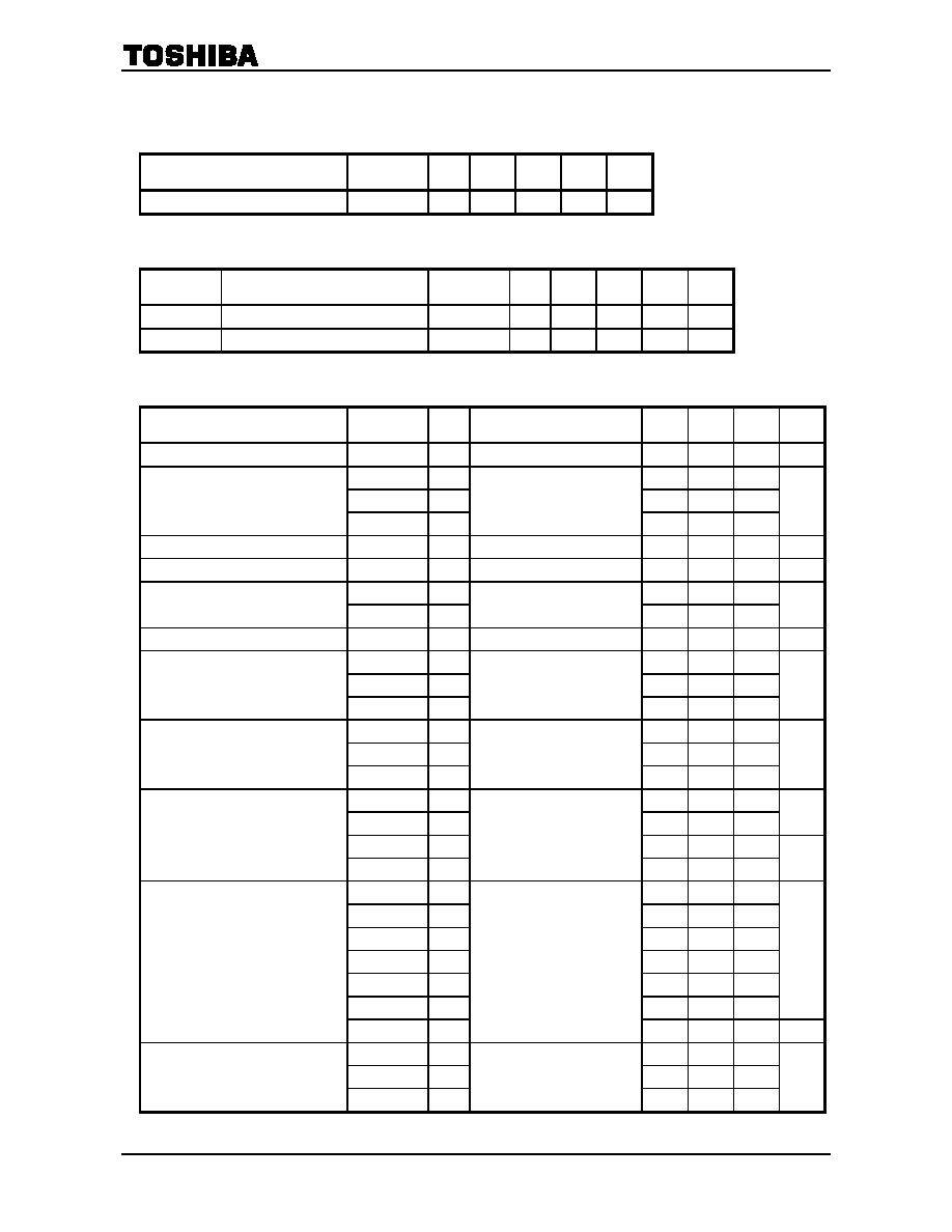
Pin 6
Pin 6 (VD
=
1)
Pin 6
Pin 11
Solid line Dashed line
Solid line Dashed line
VD
=
1
Solid line Dashed line
Solid line Dashed line

TA1317AN
2002-09-06
11
Register Name/Number of Bits
Function Explanation
Output Change
Picture Change
Preset
V-EHT COMPENSATION/3
Adjusts the compensated rate for the V-DRIVE by EHT-IN
(pin 3).
000: min
111: max
min
(000)
ANALOG V-BLK STOP PHASE/5
Sets the analog blanking stop phase on pin 20. Inputs the
output from pin 20 to an external BLK-IN of synchronization
IC.
00000: min
10000: center
11111: max
center
(10000)
H-EHT COMPENSATION/3
Adjusts the compensated rate for the EW output by EHT-IN
(pin 3).
000: min
111: max
min
(000)
ANALOG V-BLK START PHASE/5
Sets the analog blanking start phase on pin 20. Inputs the
output from pin 20 to external BLK-IN of synchronization IC.
00000: min
10000: center
11111: max
center
(10000)
V-RAMP LIMIT LEVEL/4
Sets the V-ramp slice level.
0000: OFF
0001: min
1111: max
Sub-address 05-D0 bit comes MSB.
OFF
(0000)
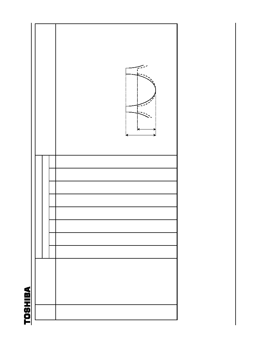
Pin 6
Solid line Dashed line
Solid line Dashed line
Solid line Dashed line
Pin 6
Solid line Dashed line
Pin 11

TA1317AN
2002-09-06
12
Register Name/Number of Bits
Function Explanation
Output Change
Picture Change
Preset
V CENTERING/7
Where VD
=
0, DC level of V-DRIVE is adjusted. Where VD
=
1, DAC output level of pin 2 is set.
0000000: min
1000000: center
1111111: max
min
(0000000)
V-DF PHASE/4
Adjusts the phase of vertical dynamic focus output.
0000: min
1000: center
1111: max
center
(1000)
V-DF AMPLITUDE/4
Adjusts the amplitude of vertical dynamic focus output.
0000: min
1000: center
1111: max
center
(1000)
H-DF PHASE/4
Adjusts the phase of horizontal dynamic focus output.
0000: min
1000: center
1111: max
center
(1000)
Pin 18
Pin 6 (VD
=
0)
Solid line
Dashed line
VD
=
0
Pin 16
Pin 18

TA1317AN
2002-09-06
13
Register Name/Number of Bits
Function Explanation
Output Change
Picture Change
Preset
H-DF AMPLITUDE/4
Adjusts the amplitude of horizontal dynamic focus output.
0000: min
1000: center
1111: max
center
(1000)
H-DF CURVE/4
Adjusts the curve characteristic of horizontal dynamic focus
output.
0000: max
1111: min
max
(0000)
V INTEGRAL CORRECTION/4
Adjusts the vertical integral correction.
0000: min
1111: max
min
(0000)
V AGC/2
Sets the AGC gain for V-ramp.
00: LOW
11: HIGH
LOW
(00)
V S CORRECTION/6
Adjusts the vertical S correction.
000000: min
100000: center
111111: max
min
(000000)
EW PARABOLA/6
Adjusts the amplitude of EW output.
000000: min
111111: max
min
(000000)
Pin 16
Pin 6
Pin 11
Solid line Dashed line
Solid line Dashed line
Pin 16
Solid line Dashed line
Pin 6

TA1317AN
2002-09-06
14
Register Name/Number of Bits
Function Explanation
Output Change
Picture Change
Preset
EW TRAPEZIUM/7
Adjusts the EW trapezium correction.
0000000: min
1000000: center
1111111: max
Note: When this data will be changed, V symmetry
characteristic will be also changed.
center
(1000000)
V STOP/1
Switches over the V-stop mode.
0: Normal
1: V stop/BLK stop
Normal
(0)
EW TOP CORNER/5
Adjusts the EW top corner correction.
00000: max
10000: center
11111: min
center
(10000)
EW BOTTOM CORNER/5
Adjusts the EW bottom corner correction.
00000: max
10000: center
11111: min
center
(10000)
EW S CORRECTION/5
Adjusts the EW S correction.
00000: max
10000: center
11111: min
center
(10000)
Pin 6
Pin 11
Solid line Dashed line
Solid line Dashed line
Pin 11
Pin 11
Solid line Dashed line
Solid line
Dashed line
Pin 11

TA1317AN
2002-09-06
15
Register Name/Number of Bits
Function Explanation
Output Change
Picture Change
Preset
EW CORNER/5
Adjusts the EW corner correction.
00000: max
10000: center
11111: min
center
(10000)
CENTER PARABOLA/4
Adjusts the parabola-component amplitude.
0000: max
1000: center
1111: min
center
(1000)
CENTER SAW/4
Adjusts the saw-component amplitude.
0000: min
1000: center
1111: max
center
(1000)
V SYMMETRY/8
Corrects the vertical symmetry.
00000000: min
10000000: center
11111111: max
Note: When this data will be changed, EW trapezium
characteristic will be also changed.
center
(10000000)
Pin 11
Solid line Dashed line
Solid line Dashed line
Solid line Dashed line
Pin 19
Pin 19
Solid line
Dashed line
Pin 6

TA1317AN
2002-09-06
16
Read Mode
Register Name/Number of Bits
Function Explanation
V DF/1
Vertical dynamic focus output self-check.
0: NG (no)
1: OK (yes)
H DF/1
Horizontal dynamic focus output self-check.
0: NG (no)
1: OK (yes)
LVP/1
LVP (low voltage protection) is detected.
0: OFF (pin 17 is high)
1: ON (pin 17 is low)
V NF/1
V-NF input self-check.
0: NG (no)
1: OK (yes)
V GUARD/1
Detects abnormality on V-NF input. If abnormal, Pin 20 goes high.
0: OFF (normal)
1: ON (abnormal)
EW OUT/1
EW output self-check.
0: NG (no)
1: OK (yes)
V OUT/1
V-DRIVE output self-check.
0: NG (no)
1: OK (yes)
POR/1 Power-on
reset.
Responds 0 at first reading after power-on, 1 at second reading.
0: Resister preset
1: Normal

TA1317AN
2002-09-06
17
Data Transfer Formats via I
2
C Bus
Slave address
A6 A5 A4 A3 A2 A1 A0 W/R
1 0 0 0 1 1 0 0/1
Start and Stop Condition
Bit Transfer
Acknowledge
SDA
SCL
S
Start condition
P
Stop condition
SDA
SCL
SDA stable
Change of SDA allowed
SDA by transmitter
Only bit 9: Low impedance
Clock pulse for acknowledge
S
1 8
9
SDA by receiver
SCL from master
Bit 9: High impedance

TA1317AN
2002-09-06
18
Data Transmit Format 1
Data Transmit Format 2
Data Receive Format
At the moment of the first acknowledge, the master transmitter becomes a master receiver and the slave
transmitter. This acknowledge is still generated by this slave.
The Stop condition is generated by the master.
Details are provided in the Philips I
2
C specifications.
Optional Data Transmit Format: Automatic Increment Mode
In this transmission method, data is set on automatically incremented sub-address from the specified
sub-address.
Purchase of TOSHIBA I
2
C components conveys a license under the Philips I
2
C Patent Rights to use these
components in an I
2
C system, provided that the system conforms to the I
2
C Standard Specification as defined by
Philips.
S
Slave address
0 A
Transmit data
A
Sub address
A P
7 bit
MSB
S: Start condition
8 bit
MSB
A: Acknowledge
9 bit
MSB
P: Stop condition
S
Slave address
0 A
Transmit data
A
Sub address
A
Transmit data n
A
Sub address
A P
S
Slave address
1 A
Transmit data 2
A
Transmit data 1
A P
7 bit
MSB
8 bit
MSB
S
Slave address
A
Transmit data 2
Transmit data 1
A P
7 bit
MSB
8 bit
MSB
0
Sub address
7 bit
MSB
A 1
8 bit
MSB

TA1317AN
2002-09-06
19
Maximum Ratings
(Ta
=
=
=
=
25∞C)
Characteristics Symbol Rating Unit
Power Supply voltage
V
CCmax
12
Input pin signal voltage
e
inmax
9
p-p
Power dissipation
P
D
(*) 1250
mW
Power dissipation reduction rate
1/
ja
-
10 mW/∞C
Operating temperature
T
opr
-
20~65 ∞C
Storage temperature
T
stg
-
55~150 ∞C
*: See the figure below.
Recommended Operating Conditions
Characteristics Description
Min
Typ.
Max
Unit
Supply voltage (V
CC
)
Pin
7
8.5 9.0 9.5 V
EHT input voltage
Pin 3
0.0
9.0 V
FBP input amplitude
Pin 12
4.0
9.0 V
FBP input frequency
Pin 12
28
45 kHz
FBP input width
Pin 12
2.5
µ
s
SCL/SDA pull-up voltage
Pins 13 & 14
3.0
5.0
9.0
V
LVP input voltage
Pin 17
0.0
9.0 V
V input amplitude
Pin 21
3.0
9.0 V
V input frequency
Pin 21
50
120 Hz
V input width
Pin 21
2.5
µ
s
EW PWM input current
Pin 8
5 mA
Figure 1 P
D
≠ Ta Curve
Ambient temperature Ta (∞C)
P
o
wer
dissi
pati
on P
D
(mW
)
1250
0
0
150
25 65
850
TA1317AN
2002-09-06
20
Electrical Characteristics
(unless otherwise specified,
V
CC
=
=
=
=
9 V, Ta
=
=
=
=
25∞C)
Current dissipation
Pin Name
Symbol
Test
Circuit
Min Typ. Max Unit
V
CC
I
CC
40 50.8 62 mA
Pin voltages
Pin No.
Pin Name
Symbol
Test
Circuit
Min Typ. Max Unit
1 V
REF
V
1
4.60 4.88 5.10 V
5 V
-DC
REF V
5
4.60 4.88 5.10 V
AC Characteristics
Characteristics Symbol
Test
Circuit
Test Condition
Min
Typ.
Max
Unit
Vertical trigger input shaped voltage
V
TH
(Note
1)
1.2 1.5 1.7 V
V
TCH
3.90 4.10 4.30
V
TCM
2.95 3.15 3.35
Timing pulse output voltage
V
TCL
(Note 2)
0.97 1.07 1.17
V
Vertical ramp wave amplitude
V
RMP
(Note
3)
1.65 1.75 1.85 V
p-p
Vertical drive amplification
GV
(Note
4)
21 24 27 dB
V
4H
2.5 3.3 4.1
Vertical drive output voltage
V
4L
(Note 5)
0.00 0.00 0.30
V
Vertical NF signal amplitude
V
NFM
(Note
6)
1.65 1.85 2.05 V
p-p
V
DC
(80)
3.00 3.55 4.10
V
DC
(83)
5.65 6.20 6.75
Vertical phase adjustment 1 (V shift)
change amount
V
DC
(Note 7)
2.30 2.65 3.00
V
V
DD
(00)
1.64 1.82 2.00
V
DD
(FE)
2.87 3.16 3.45
Vertical phase adjustment 2
(V centering) change amount
V
DD
(Note 8)
1.30 1.45 1.60
V
V
NFL
0.85 1.00 1.15
V
NFH
2.55 2.75 2.95
V
p-p
V
NFP
43 48 53
Vertical amplitude adjustment
(picture height) change amount
V
NFN
(Note 9)
-
53
-
48
-
43
%
V
1
(00)
0.90 1.06 1.22
V
2
(00)
0.69 0.81 0.93
V
1
(80)
0.82 0.96 1.10
V
2
(80)
0.77 0.91 1.05
V
1
(F8)
0.73 0.86 0.99
V
2
(F8)
0.85 1.00 1.15
V
p-p
Vertical linearity correction
(V linearity) change amount
V
LIN
(Note 10)
9.5 10.5 12.5 %
V
VT
(00)
4.60 4.95 5.20
V
VT
(FF)
5.40 5.70 6.00
Vertical symmetry (V symmetry)
change amount
V
VT
(Note 11)
0.67 0.76 0.85
V

TA1317AN
2002-09-06
21
Characteristics Symbol
Test
Circuit
Test Condition
Min
Typ.
Max
Unit
V
S
(80)
1.92 2.26 2.60
V
S
(BF)
1.27 1.50 1.73
V
p-p
Vertical S correction (V S correction)
change amount
V
S
(Note 12)
17 21 25 %
V
(80)
1.54 1.82 2.10
V
(8F)
1.62 1.90 2.18
V
p-p
Vertical integral correction
(V
correction) change amount
V
(Note 13)
3.0 4.0 5.2 %
V
E
(80)
1.58 1.86 2.14
V
E
(87)
1.44 1.69 1.94
V
p-p
Vertical EHT compensation (V EHT
compensation) change amount
V
EHT
(Note 14)
8.5 10.0 11.5 %
V
EHL
1.9 2.4 2.9
EHT input dynamic range
V
EHH
(Note 15)
5.9 6.4 6.9
V
V
EV
(00)
5.20 6.15 7.10
V
EV
(FC)
1.30 1.55 1.80
Horizontal amplitude adjustment
(picture width) change amount
V
EV
(Note 16)
4.20 4.60 5.00
V
V
PB
(00)
0.00 0.02 0.06
V
PB
(20)
1.6 2.0 2.3
V
PB
(3F)
2.8 3.3 3.8
Parabola amplitude adjustment
(EW parabola) change amount
V
PB
(Note 17)
2.8 3.3 3.8
V
p-p
V
TC
(00)
2.3 2.8 3.2
V
TC
(F8)
0.9 1.2 1.4
V
p-p
V
TCP
32 40 46
EW top corner correction
(EW top corner) change amount
V
TCN
(Note 18)
-
46
-
40
-
32
%
V
BC
(00)
2.4 2.8 3.2
V
BC
(F8)
0.9 1.2 1.4
V
p-p
V
BCP
32 45 55
EW bottom corner correction
(EW bottom corner) change amount
V
BCN
(Note 19)
-
52
-
40
-
35
%
V
M
(00)
2.4 2.8 3.2
V
M
(F8)
0.8 1.1 1.4
V
p-p
V
MP
40 47 57
EW corner correction change amount
V
MN
(Note 20)
-
52
-
42
-
32
%
V
S
(00)
2.2 2.6 3.0
V
S
(F8)
1.0 1.4 1.6
V
p-p
V
SP
28 35 40
EW S correction change amount
V
SN
(Note 21)
-
40
-
32
-
27
%
V
ET
(00)
2.4 2.7 3.0
V
ET
(FE)
-
3.0
-
2.7
-
2.4
ms
V
ETP
11.0 13.5 16.0
EW trapezium correction change
amount
V
ETN
(Note 22)
-
16.0
-
13.5
-
11.0
%
V
HC
(80)
3.0 3.6 4.2
V
HC
(87)
4.0 4.7 5.4
Horizontal EHT compensation (H-EHT
compensation) DC change amount
V
HC
(Note 23)
1.0 1.2 1.4
V
EHT (1)
1.55 1.90 2.20
EHT (7)
1.65 2.00 2.30
V
p-p
Parabola amplitude EHT
compensation
EHT
(Note 24)
2.7 4.0 5.3 %

TA1317AN
2002-09-06
22
Characteristics Symbol
Test
Circuit
Test Condition
Min
Typ.
Max
Unit
V
X
(00)
20 35 50
V
X
(40)
45 65 85
V
X
(80)
250 340 430
AGC operating current
V
X
(C0)
(Note 25)
535 715 895
µ
A
V
N
(8F)
4.3 5.0 5.7
Sawtooth correction (cent saw)
maximum amplitude
V
N
(80)
(Note 26)
4.3 5.0 5.7
V
p-p
V
P
(F8)
1.9 2.2 2.5
Parabola correction (cent par)
maximum amplitude
V
P
(08)
(Note 27)
1.9 2.2 2.5
V
p-p
V
HD
(80)
2.1 2.8 3.3
V
HD
(88)
2.4 3.1 4.0
V
HD
(8F)
2.6 3.4 4.3
V
p-p
V
HDP
7
10
13
Horizontal DF amplitude adjustment
(H DF amp)
V
HDN
(Note 28)
-
15
-
12
-
7
%
T
HD
(08)
-
6.0
-
4.4
-
2.0
T
HD
(F8)
2.0 4.4 6.0
Horizontal DF phase adjustment
(H DF phase)
T
HD
(Note 29)
6.5 8.8 10.0
V
p-p
T
HB
(00)
32.0 42.0 52.0
T
HB
(F0)
21.0 31.0 41.0
Horizontal DF bathtub (H DF curve)
adjustment
T
HB
(Note 30)
2.5 4.5 6.5
µ
s
V
VD
(80)
2.05 2.40 2.75
V
VD
(88)
2.30 2.70 3.10
V
VD
(8F)
2.55 3.00 3.45
V
p-p
V
VDP
7
10
13
Vertical DF amplitude adjustment
(V DF amp)
V
VDN
(Note 31)
-
15
-
10
-
7
%
T
VD
(08)
-
2.5
-
2.0
-
1.5
T
VD
(F8)
1.5 2.0 2.5
Vertical DF phase adjustment
(V DF phase)
T
VD
(Note 32)
3.4 4.0 4.6
ms
LVP detection voltage
V
LVP
(Note
33)
4.7 5.0 5.3 V
V
VGH
7.0 7.3 7.6
Vertical guard detection voltage
V
VGL
(Note 34)
2.1 2.4 2.7
V
Vertical guard detection output current
(BLK-OUT output current)
I
20
(Note
35)
450 630 750
µ
A
V
CA
(00)
0.20 0.50 0.55
Vertical centering DAC output voltage
1 (V centering)
V
CA
(FE)
(Note 36)
4.7 5.0 5.3
V
V
CD
(80)
0.20 0.60 0.80
Vertical centering DAC output voltage
2 (V shift)
V
CD
(83)
(Note 37)
4.7 5.0 5.3
V
V
Y
(00)
1.7 1.9 2.1
V
Y
(80)
2.25 2.50 2.75
Vertical centering change amount in V
STOP mode
V
Y
(FE)
(Note 38)
2.7 3.0 3.3
V
Vertical NF signal amplitude at DC
coupling
V
DFB
(Note
39)
0.85 0.95 1.05 V
p-p
Vertical NF center voltage at DC
coupling
V
C
(Note
40)
2.25 2.50 2.75 V

TA1317AN
2002-09-06
23
Characteristics Symbol
Test
Circuit
Test Condition
Min
Typ.
Max
Unit
V
CHH
20.0 26.0 32.0
Vertical ramp cut level
V
CLH
(Note 41)
26.0 32.1 38.0
%
BLHL
5.05 5.90 6.75
BLHM
2.30 2.70 3.10
BLHH
0.00
0.10
BLLL
5.10 6.00 6.90
BLLM
2.05 2.40 3.00
Analog blanking phase
BLLH
(Note 42)
0.00
0.10
ms
V
PP
(00)
0.00 0.02 0.06
V
PP
(20)
1.6 2.00 2.30
V
PP
(3F)
2.80 3.30 3.80
Parabola amplitude adjustment (EW
parabola) change amount at PWM
V
PP
(Note 43)
2.80 3.30 3.80
V
p-p

TA1317AN
2002-09-06
24
Test Condition
Test Condition
SW Mode
Note
No.
Parameter
SW5 SW6 SW7 SW8 SW10
SW11
SW17
SW24
Test Method
(unless otherwise specified, V
CC
=
9 V, Ta
=
25
±
3∞C, data
=
preset values)
1
Vertical trigger input shaped
voltage
OFF
B
ON
OFF
B
ON
A
A
(1) Input vertical trigger pulse (figure below) to pin V
IN
.
(2) Increase vertical trigger pulse level (VT) from 0 V
P-P
. When timing pulse is output to
pin 22 (TC FILTER), measure vertical trigger pulse level V
TH
.
2
Timing pulse output voltage
OFF
B
ON
OFF
B
ON
A
A
(1) Input vertical trigger pulse to pin V
IN
.
Pulse
level
(VT)
=
3.0 V
(2) Measure pin 22 (TC FILTER) voltages (V
TCH
, V
TCM
, V
TCL
) as shown in the figure
below.
Pin 22
(TC FILTER) waveform
Pin 23
(V-RAMP FILTER) waveform
V
TCH
V
TCM
V
TCL
640
µ
s
Vertical cycle
=
20
Vertical trigger pulse
Pulse level (VT)
0 V

TA1317AN
2002-09-06
25
Test Condition
SW Mode
Note
No.
Parameter
SW5 SW6 SW7 SW8 SW10
SW11
SW17
SW24
Test Method
(unless otherwise specified, V
CC
=
9 V, Ta
=
25
±
3∞C, data
=
preset values)
3
Vertical ramp wave amplitude
OFF
B
ON
OFF
B
ON
A
A
(1) Input vertical trigger pulse to pin V
IN
.
Pulse
level
(VT)
=
3.0 V
(2) Measure pin 23 (V-RAMP FILTER) amplitude V
RMP
as shown in the figure below.
4
Vertical drive amplification
OFF
C
ON
OFF
B
ON
A
A
(1) No signal input to pin V
IN
.
(2) Set VD (V-DRIVE mode switch) (sub-address: 00) to AC-Coupling mode (data: 81).
(3) Connect external power supply (V
6
) to TP6 (V fb).
(4) Change external power supply (V
6
) until pin 4 (V DRIVE) voltage is 0.8 V.
The voltage is made V
6A
.
(5) Measure pin 4 voltage (V
4A
) when the external power supply voltage is V
6A
+
0.2 V.
(6) Calculate the drive amplification (GV) using the following formula.
V
4A
-
0.8
GV
=
20 og
0.2
V
RMP
Pin 23
(V-RAMP FILTER) waveform
P
i
n 4
(V
DR
I
V
E
)
vol
t
age
(V
4
)
Pin 6 (V NF) external supply voltage (V
6
)
V
4H
V
4L
V
4A
0.8 V
V
6A
V
6A
+
0.2 V

TA1317AN
2002-09-06
26
Test Condition
SW Mode
Note
No.
Parameter
SW5 SW6 SW7 SW8 SW10
SW11
SW17
SW24
Test Method
(unless otherwise specified, V
CC
=
9 V, Ta
=
25
±
3∞C, data
=
preset values)
5
Vertical drive output voltage
OFF
C
ON
OFF
B
ON
A
A
(1) Measure V
4H
using the figure for Note 4.
(2) Measure V
4L
using the figure for Note 4.
6
Vertical NF signal amplitude
OFF
C
ON
OFF
B
ON
A
A
(1) Input vertical trigger pulse to pin V
IN
.
Pulse
level
(VT)
=
3.0 V
(2) Set VD (sub-address: 00) to AC-Coupling mode (data: 81).
(3) Set V INTEGRAL CORRECTION (sub-address: 08) to center (data: 88).
(4) Set V S CORRECTION (sub-address: 09) to center (data: A0).
(5) Set V SHIFT (sub-address: 01) data to 82.
(6) Measure Pin 6 (V NF) vertical sawtooth amplitude V
NFM
.
V
NFM
Pin 6
(V NF) waveform

TA1317AN
2002-09-06
27
Test Condition
SW Mode
Note
No.
Parameter
SW5 SW6 SW7 SW8 SW10
SW11
SW17
SW24
Test Method
(unless otherwise specified, V
CC
=
9 V, Ta
=
25
±
3∞C, data
=
preset values)
7
Vertical phase adjustment 1
(V shift) change amount
OFF
B
ON
OFF
B
ON
A
A
(1) Input vertical trigger pulse to pin V
IN
.
Pulse
level
(VT)
=
3.0 V
(2) Set VD (sub-address: 00) to AC-Coupling mode (data: 81).
(3) Set V INTEGRAL CORRECTION (sub-address: 08) to center (data: 88).
(4) Set V S CORRECTION (sub-address: 09) to center (data: A0).
(5) Set V SHIFT (sub-address: 01) to minimum (data: 80) and measure V
DC
(80) as
shown in the figure below.
(6) Set V SHIFT (sub-address: 01) to maximum (data: 83) and measure V
DC
(83) as
shown in the figure below.
(7) Calculate change amount V
DC
using the following formula.
V
DC
=
V
DC
(83)
-
V
DC
(80)
V
DC
(83)
V
DC
(80)
10 ms
Pin 6
(V NF) waveform
10 ms

TA1317AN
2002-09-06
28
Test Condition
SW Mode
Note
No.
Parameter
SW5 SW6 SW7 SW8 SW10
SW11
SW17
SW24
Test Method
(unless otherwise specified, V
CC
=
9 V, Ta
=
25
±
3∞C, data
=
preset values)
8
Vertical phase adjustment 2
(V centering) change amount
ON
A
OFF
OFF
B
ON
A
A
(1) Input vertical trigger pulse to pin V
IN
.
Pulse
level
(VT)
=
3.0 V
(2) Set VD (sub-address: 00) to DC-Coupling mode (data: 80).
(3) Set V INTEGRAL CORRECTION (sub-address: 08) to center (data: 88).
(4) Set V S CORRECTION (sub-address: 09) to center (data: A0).
(5) Set V CENTERING (sub-address: 05) to minimum (data: 00) and measure V
DD
(00)
as shown in the figure below.
(6) Set V CENTERING (sub-address: 05) to maximum (data: FE) and measure V
DD
(FE) as shown in the figure below.
(7) Calculate change amount V
DD
using the following formula.
V
DD
=
V
DD
(FE)
-
V
DD
(00)
V
DD
(FE)
V
DD
(00)
10 ms
Pin 6
(V NF) waveform
10 ms

TA1317AN
2002-09-06
29
Test Condition
SW Mode
Note
No.
Parameter
SW5 SW6 SW7 SW8 SW10
SW11
SW17
SW24
Test Method
(unless otherwise specified, V
CC
=
9 V, Ta
=
25
±
3∞C, data
=
preset values)
9
Vertical amplitude adjustment
(picture height) change
amount
OFF
B
ON
OFF
B
ON
A
A
(1) Input vertical trigger pulse to pin V
IN
.
Pulse
level
(VT)
=
3.0 V
(2) Set VD (sub-address: 00) to AC-Coupling mode (data: 81).
(3) Set V INTEGRAL CORRECTION (sub-address: 08) to center (data: 88).
(4) Set V S CORRECTION (sub-address: 09) to center (data: A0).
(5) Set V SHIFT (sub-address: 01) data to 82.
(6) Set PICTURE HEIGHT (sub-address: 00) to minimum (data: 01) and measure Pin 6
(V NF) amplitude (V
NFL
).
(7) Set PICTURE HEIGHT (sub-address: 00) to maximum (data: FF) and measure Pin
6 (V NF) amplitude (V
NFH
).
(8) Determine variable ranges (V
NFP
, V
NFN
) using the following formulas.
V
NFH
-
V
NFM
V
NFL
-
V
NFM
V
NFP
=
V
NFM
◊
100,
V
NFN
=
V
NFM
◊
100
V
NF
L
V
NF
H
Pin 6
(V NF) waveform

TA1317AN
2002-09-06
30
Test Condition
SW Mode
Note
No.
Parameter
SW5 SW6 SW7 SW8 SW10
SW11
SW17
SW24
Test Method
(unless otherwise specified, V
CC
=
9 V, Ta
=
25
±
3∞C, data
=
preset values)
10 Vertical
linearity
correction
(V linearity) change amount
OFF
B
ON
OFF
B
ON
A
A
(1) Input vertical trigger pulse to pin V
IN
.
Pulse
level
(VT)
=
3.0 V
(2) Set VD (sub-address: 00) to AC-Coupling mode (data: 81).
(3) Set V INTEGRAL CORRECTION (sub-address: 08) to center (data: 88).
(4) Set V S CORRECTION (sub-address: 09) to center (data: A0).
(5) Set V SHIFT (sub-address: 01) data to 82.
(6) Set V LINEARITY (sub-address: 02) to minimum (data: 00) and measure V
1
(00)
and V
2
(00) as shown in the figure below.
(7) Set V LINEARITY (sub-address: 02) to center (data: 80) and measure V
1
(80) and
V
2
(80) as shown in the figure below.
(8) Set V LINEARITY (sub-address: 02) to maximum (data: F8) and measure V
1
(F8)
and V
2
(F8) as shown in the figure below.
(9) Calculate maximum correction V
LIN
from measured result using the following
formula.
V
1
(00)
-
V
1
(F8)
+
V
2
(F8)
-
V
2
(00)
V
LIN
=
2
◊
[V
1
(80)
+
V
2
(80)]
◊
100
V
1
(
**
)
V
2
(
**
)
10 ms
Pin 6
(V NF) waveform
10 ms

TA1317AN
2002-09-06
31
Test Condition
SW Mode
Note
No.
Parameter
SW5 SW6 SW7 SW8 SW10
SW11
SW17
SW24
Test Method
(unless otherwise specified, V
CC
=
9 V, Ta
=
25
±
3∞C, data
=
preset values)
11 Vertical
symmetry
(V symmetry) change amount
OFF
B
ON
OFF
B
ON
A
A
(1) Input vertical trigger pulse to pin V
IN
.
Pulse
level
(VT)
=
3.0 V
(2) Set VD (sub-address: 00) to AC-Coupling mode (data: 81).
(3) Set V INTEGRAL CORRECTION (sub-address: 08) to center (data: 88).
(4) Set V S CORRECTION (sub-address: 09) to center (data: A0).
(5) Set V SHIFT (sub-address: 01) data to 82.
(6) Set V SYMMETRY (sub-address: 11) to minimum (data: 00) and measure Pin 6 (V
NF) voltage V
VT
(00).
(7) Set V SYMMETRY (sub-address: 11) to maximum (data: FF) and measure Pin 6 (V
NF) voltage V
VT
(FF).
(8) Calculate change amount V
VT
using the following formula.
V
VT
=
V
VT
(FF)
-
V
VT
(00)
V
VT
(00)
V
VT
(FF)
10 ms
Pin 6
(V NF) waveform
10 ms

TA1317AN
2002-09-06
32
Test Condition
SW Mode
Note
No.
Parameter
SW5 SW6 SW7 SW8 SW10
SW11
SW17
SW24
Test Method
(unless otherwise specified, V
CC
=
9 V, Ta
=
25
±
3∞C, data
=
preset values)
12
Vertical S correction (V S
correction) change amount
OFF
B
ON
OFF
B
ON
A
A
(1) Input vertical trigger pulse to pin V
IN
.
Pulse
level
(VT)
=
3.0 V
(2) Set VD (sub-address: 00) to AC-Coupling mode (data: 81).
(3) Set V INTEGRAL CORRECTION (sub-address: 08) to center (data: 88).
(4) Set V SHIFT (sub-address: 01) to 82.
(5) Set V S CORRECTION (sub-address: 09) to minimum (data: 80) and measure V
S
(80) as shown in the figure below.
(6) Set V S CORRECTION (sub-address: 09) to maximum (data: BF) and measure V
S
(BF) as shown in the figure below.
(7) Calculate maximum correction V
S
using measured result and the following formula.
V
S
(80)
-
V
S
(8F)
V
S
=
V
S
(80)
+
V
S
(8F)
◊
100
V
S
(80)
V
S
(B
F
)
Pin 6
(V NF) waveform

TA1317AN
2002-09-06
33
Test Condition
SW Mode
Note
No.
Parameter
SW5 SW6 SW7 SW8 SW10
SW11
SW17
SW24
Test Method
(unless otherwise specified, V
CC
=
9 V, Ta
=
25
±
3∞C, data
=
preset values)
13 Vertical
integral
correction
(V
correction) change
amount
OFF
B
ON
OFF
B
ON
A
A
(1) Input vertical trigger pulse to pin V
IN
.
Pulse
level
(VT)
=
3.0 V
(2) Set VD (sub-address: 00) to AC-Coupling mode (data: 81).
(3) Set V S CORRECTION (sub-address: 09) to center (data: A0).
(4) Set V SHIFT (sub-address: 01) to 82.
(5) Set V INTEGRAL CORRECTION (sub-address: 08) to minimum (data: 80) and
measure V
(80) as shown in the figure below.
(6) Set V INTEGRAL CORRECTION (sub-address: 08) to maximum (data: 8F) and
measure V
(8F) as shown in the figure below.
(7) Calculate maximum correction V
from measured result using the following
formula.
V
(8F)
-
V
(80)
V
=
V
(80)
◊
100
Pin 6
(V NF) waveform
V
(8F)
V
(80)

TA1317AN
2002-09-06
34
Test Condition
SW Mode
Note
No.
Parameter
SW5 SW6 SW7 SW8 SW10
SW11
SW17
SW24
Test Method
(unless otherwise specified, V
CC
=
9 V, Ta
=
25
±
3∞C, data
=
preset values)
14
Vertical EHT compensation
(V EHT compensation)
change amount
OFF
B
ON
OFF
B
ON
A
A
(1) Input vertical trigger pulse to pin V
IN
.
Pulse
level
(VT)
=
3.0 V
(2) Set VD (sub-address: 00) to AC-Coupling mode (data: 81).
(3) Set V SHIFT (sub-address: 01) data to 82.
(4) Connect external power supply (DC voltage
=
0 V) to pin 3 (EHT IN).
(5) Set V-EHT COMPENSATION (sub-address: 02) to minimum (data: 80) and
measure Pin 6 (V NF) amplitude V
E
(80).
(6) Set V-EHT COMPENSATION (sub-address: 02) to maximum (data: 87) and
measure Pin 6 (V NF) amplitude V
E
(87).
(7) Calculate change amount V
EHT
using the following formula.
V
E
(80)
-
V
E
(87)
V
EHT
=
V
E
(87)
◊
100

TA1317AN
2002-09-06
35
Test Condition
SW Mode
Note
No.
Parameter
SW5 SW6 SW7 SW8 SW10
SW11
SW17
SW24
Test Method
(unless otherwise specified, V
CC
=
9 V, Ta
=
25
±
3∞C, data
=
preset values)
15
EHT input dynamic range
OFF
B
ON
OFF
B
ON
A
A
(1) Input vertical trigger pulse to pin V
IN
.
Pulse
level
(VT)
=
3.0 V
(2) Set VD (sub-address: 00) to AC-Coupling mode (data: 81).
(3) Set V SHIFT (sub-address: 01) data to 82.
(4) Connect external power supply V
3
to pin 3 (EHT IN).
(5) Set V-EHT COMPENSATION (sub-address: 02) to maximum (data: 87).
(6) Change external power supply V
3
from 1 to 7 V and monitor Pin 6 (V NF)
amplitude.
(7) When Pin 6 (V NF) amplitude changes, measure V
3
voltages V
EHL
and V
EHH
.
16 Horizontal
amplitude
adjustment (picture width)
change amount
OFF
B
ON
OFF
B
ON
A
A
(1) Input vertical trigger pulse to pin V
IN
.
Pulse
level
(VT)
=
3.0 V
(2) Set EW PARABOLA (sub-address: 0A) to minimum (data: 00).
(3) Set PICTURE WIDTH to maximum ( (sub-address: 01, data: FC) and (sub-address:
0C, data: 81) ) and measure Pin 10 (EW FD) voltage V
EV
(FC).
(4) Set PICTURE WIDTH to minimum ( (sub-address: 01, data: 00) and (sub-address:
0C, data: 80) ) and measure Pin 10 (EW FD) voltage V
EV
(00).
(5) Calculate change amount V
EV
using the following formula.
V
EV
=
V
EV
(FC)
-
V
EV
(00)
Voltage applied to pin 3 (EHT IN) (V
3
)
P
i
n 6
(V
NF)
a
m
pl
i
t
ude
V
EHL
V
EHH
TA1317AN
2002-09-06
36
Test Condition
SW Mode
Note
No.
Parameter
SW5 SW6 SW7 SW8 SW10
SW11
SW17
SW24
Test Method
(unless otherwise specified, V
CC
=
9 V, Ta
=
25
±
3∞C, data
=
preset values)
17 Parabola
amplitude
adjustment (EW parabola)
change amount
OFF
B
ON
OFF
B
ON
A
A
(1) Input vertical trigger pulse to pin V
IN
.
Pulse
level
(VT)
=
3.0 V
(2) Set PICTURE WIDTH (sub-address: 01) to maximum (data: FC).
(3) Apply external power supply (DC voltage
=
7 V) to pin 3 (EHT IN).
(4) Set EW PARABOLA (sub-address: 0A) to minimum (data: 00) and measure Pin 10
(EW FD) amplitude V
PB
(00).
(5) Set EW PARABOLA (sub-address: 0A) to center (data: 20) and measure Pin 10
(EW FD) amplitude V
PB
(20).
(6) Set EW PARABOLA (sub-address: 0A) to maximum (data: 3F) and measure Pin 10
(EW FD) amplitude V
PB
(3F).
(7) Calculate change amount V
PB
using the following formula.
V
PB
=
V
PB
(3F)
-
V
PB
(00)
Pin 10 (EW FD) waveform
V
PB
(00)
V
PB
(3F
)

TA1317AN
2002-09-06
37
Test Condition
SW Mode
Note
No.
Parameter
SW5 SW6 SW7 SW8 SW10
SW11
SW17
SW24
Test Method
(unless otherwise specified, V
CC
=
9 V, Ta
=
25
±
3∞C, data
=
preset values)
18
EW top corner correction (EW
top corner) change amount
OFF
B
ON
OFF
B
ON
A
A
(1) Input vertical trigger pulse to pin V
IN
.
Pulse
level
(VT)
=
3.0 V
(2) Apply external power supply (DC voltage
=
7 V) to pin 3 (EHT IN).
(3) Set EW PARABOLA (sub-address: 0A) to center (data: 20).
(4) Set EW TOP CORNER (sub-address: 0C) to minimum (data: 00) and measure Pin
10 (EW FD) amplitude V
TC
(00).
(5) Set EW TOP CORNER (sub-address: 0C) to maximum (data: F8) and measure Pin
10 (EW FD) amplitude V
TC
(F8).
(6) Calculate change amounts V
TCP
and V
TCN
using the following formulas.
V
TC
(00)
-
V
PB
(20)
V
TCP
=
V
PB
(20)
◊
100
V
TC
(F8)
-
V
PB
(20)
V
TCN
=
V
PB
(20)
◊
100
VT
C(
F8
VT
C(
00
Pin 10 (EW FD) waveform
V
TC
(F
8)
V
TC
(00)

TA1317AN
2002-09-06
38
Test Condition
SW Mode
Note
No.
Parameter
SW5 SW6 SW7 SW8 SW10
SW11
SW17
SW24
Test Method
(unless otherwise specified, V
CC
=
9 V, Ta
=
25
±
3∞C, data
=
preset values)
19
EW bottom corner correction
(EW bottom corner) change
amount
OFF
B
ON
OFF
B
ON
A
A
(1) Input vertical trigger pulse to pin V
IN
.
Pulse
level
(VT)
=
3.0 V
(2) Apply external power supply (DC voltage
=
7 V) to pin 3 (EHT IN).
(3) Set EW PARABOLA (sub-address: 0A) to center (data: 20).
(4) Set EW BTM CORNER (sub-address: 0D) to minimum (data: 00) and measure Pin
10 (EW FD) amplitude V
BC
(00).
(5) Set EW BTM CORNER (sub-address: 0D) to maximum (data: F8) and measure Pin
10 (EW FD) amplitude V
BC
(F8).
(6) Calculate change amounts V
BCP
and V
BCN
using the following formulas.
V
BC
(00)
-
V
PB
(20)
V
BCP
=
V
PB
(20)
◊
100
V
BC
(F8)
-
V
PB
(20)
V
BCN
=
V
PB
(20)
◊
100
VT
C(
F8
VT
C(
00
Pin 10 (EW FD) waveform
V
BC
(F
8)
V
BC
(00)

TA1317AN
2002-09-06
39
Test Condition
SW Mode
Note
No.
Parameter
SW5 SW6 SW7 SW8 SW10
SW11
SW17
SW24
Test Method
(unless otherwise specified, V
CC
=
9 V, Ta
=
25
±
3∞C, data
=
preset values)
20
EW corner correction change
amount
OFF
B
ON
OFF
B
ON
A
A
(1) Input vertical trigger pulse to pin V
IN
.
Pulse
level
(VT)
=
3.0 V
(2) Apply external power supply (DC voltage
=
7 V) to pin 3 (EHT IN).
(3) Set EW PARABOLA (sub-address: 0A) to center (data: 20).
(4) Set EW CORNER (sub-address: 0F) to minimum (data: 00) and measure Pin 10
(EW FD) amplitude V
M
(00).
(5) Set EW CORNER (sub-address: 0F) to maximum (data: F8) and measure Pin 10
(EW FD) amplitude V
M
(F8).
(6) Calculate change amounts V
MP
and V
MN
using the following formulas.
V
M
(00)
-
V
PB
(20)
V
MP
=
V
PB
(20)
◊
100
V
M
(F8)
-
V
PB
(20)
V
MN
=
V
PB
(20)
◊
100
Pin 10 (EW FD) waveform
V
M
(F
8)
V
M
(00)

TA1317AN
2002-09-06
40
Test Condition
SW Mode
Note
No.
Parameter
SW5 SW6 SW7 SW8 SW10
SW11
SW17
SW24
Test Method
(unless otherwise specified, V
CC
=
9 V, Ta
=
25
±
3∞C, data
=
preset values)
21
EW S correction change
amount
OFF
B
ON
OFF
B
ON
A
A
(1) Input vertical trigger pulse to pin V
IN
.
Pulse
level
(VT)
=
3.0 V
(2) Apply external power supply (DC voltage
=
7 V) to pin 3 (EHT IN).
(3) Set EW PARABOLA (sub-address: 0A) to center (data: 20).
(4) Set S CORRECTION (sub-address: 0E) to minimum (data: 00) and measure Pin 10
(EW FD) amplitude V
S
(00).
(5) Set S CORRECTION (sub-address: 0E) to maximum (data: F8) and measure Pin
10 (EW FD) amplitude V
S
(F8).
(6) Calculate change amounts V
SP
and V
SN
using the following formulas.
V
S
(00)
-
V
PB
(20)
V
SP
=
V
PB
(20)
◊
100
V
S
(F8)
-
V
PB
(20)
V
SN
=
V
PB
(20)
◊
100
Pin 10 (EW FD) waveform
V
S
(F
8)
V
S
(00)

TA1317AN
2002-09-06
41
Test Condition
SW Mode
Note
No.
Parameter
SW5 SW6 SW7 SW8 SW10
SW11
SW17
SW24
Test Method
(unless otherwise specified, V
CC
=
9 V, Ta
=
25
±
3∞C, data
=
preset values)
22
EW trapezium correction
change amount
OFF
B
ON
OFF
B
ON
A
A
(1) Input vertical trigger pulse to pin V
IN
.
Pulse
level
(VT)
=
3.0 V
(2) Apply external power supply (DC voltage
=
7 V) to pin 3 (EHT IN).
(3) Set EW PARABOLA (sub-address: 0A) to maximum (data: 3F).
(4) Set EW TRAPEZIUM (sub-address: 0B) to minimum (data: 00) and measure Pin 10
(EW FD) phase V
ET
(00).
(5) Set EW TRAPEZIUM (sub-address: 0B) to maximum (data: FE) and measure Pin
10 (EW FD) phase V
ET
(FE).
(6) Calculate change amounts V
ETP
and V
ETN
using the following formulas.
V
ET
(FE)
V
ETP
=
20
◊
100
V
ET
(00)
V
ETN
=
20
◊
100
Pin 10 (EW FD) waveform
V
ET
(00)
V
ET
(FE)

TA1317AN
2002-09-06
42
Test Condition
SW Mode
Note
No.
Parameter
SW5 SW6 SW7 SW8 SW10
SW11
SW17
SW24
Test Method
(unless otherwise specified, V
CC
=
9 V, Ta
=
25
±
3∞C, data
=
preset values)
23
Horizontal EHT compensation
(H-EHT compensation) DC
change amount
OFF
B
ON
OFF
B
ON
A
A
(1) Input vertical trigger pulse to pin V
IN
.
Pulse
level
(VT)
=
3.0 V
(2) Apply external power supply (DC voltage
=
1 V) to pin 3 (EHT IN).
(3) Set H-EHT COMPENSATION (sub-address: 03) to minimum (data: 80) and
measure Pin 10 (EW FD) amplitude V
HC
(80).
(4) Set H-EHT COMPENSATION (sub-address: 03) to maximum (data: 87) and
measure Pin 10 (EW FD) amplitude V
HC
(87).
(5) Calculate change amount V
HC
using the following formula.
V
HC
=
V
HC
(87)
-
V
HC
(80)
Pin 10 (EW FD) waveform
V
HC
(80)
V
HC
(87)

TA1317AN
2002-09-06
43
Test Condition
SW Mode
Note
No.
Parameter
SW5 SW6 SW7 SW8 SW10
SW11
SW17
SW24
Test Method
(unless otherwise specified, V
CC
=
9 V, Ta
=
25
±
3∞C, data
=
preset values)
24 Parabola
amplitude
EHT
compensation
OFF
B
ON
OFF
B
ON
A
A
(1) Input vertical trigger pulse to pin V
IN
.
Pulse
level
(VT)
=
3.0 V
(2) Apply external power supply V
3
to pin 3 (EHT IN).
(3) Set EW PARABOLA (sub-address: 0A) to center (data: 20).
(4) Set external power supply V
3
to 7 V and measure Pin 10 (EW FD) amplitude EHT
(7).
(5) Set external power supply V
3
to 1 V and measure Pin 10 (EW FD) amplitude EHT
(1).
(6) Calculate change amount EHT using the following formula.
EHT (7)
-
EHT (1)
EHT
=
EHT (7)
◊
100
25
AGC operating current
OFF
B
ON
OFF
B
ON
A
B
(1) Input vertical trigger pulse to pin V
IN
.
Pulse
level
(VT)
=
3.0 V
(2) When V AGC (sub-address: 09) is switched, set data to 00, 40, 80, and C0 and
measure the following.
(3) Connect external power supply 2 V through 2 k
to pin 24 (AGC FILTER).
(4) Monitor pin 24 (AGC FILTER) and measure pulse levels V
X
(00), V
X
(40), V
X
(80),
and V
X
(C0) as shown in the figure below.
(5) Calculate output currents (I
X
(00), I
X
(40), I
X
(80), I
X
(C0) using the following
formula.
V
X
(**)
I
X
(**)
=
2 k
Pin 24 (AGC FILTER) waveform
V
X

TA1317AN
2002-09-06
44
Test Condition
SW Mode
Note
No.
Parameter
SW5 SW6 SW7 SW8 SW10
SW11
SW17
SW24
Test Method
(unless otherwise specified, V
CC
=
9 V, Ta
=
25
±
3∞C, data
=
preset values)
26 Sawtooth
correction
(cent saw) maximum
amplitude
OFF
B
ON
OFF
B
ON
A
A
(1) Input vertical trigger pulse to pin V
IN
.
Pulse
level
(VT)
=
3.0 V
(2) Set CENTER SAW (sub-address: 10) to maximum (data: 8F) and measure pin 19
(CENT OUT) amplitude V
N
(8F).
(3) Set CENTER SAW (sub-address: 10) to minimum (data: 80) and measure pin 19
(CENT OUT) amplitude V
N
(80).
27
Parabola correction (cent par)
maximum amplitude
OFF
B
ON
OFF
B
ON
A
A
(1) Input vertical trigger pulse to pin V
IN
.
Pulse
level
(VT)
=
3.0 V
(2) Set CENTER PARABOLA (sub-address: 10) to maximum (data: F8) and measure
pin 19 (CENT OUT) amplitude V
P
(F8).
(3) Set CENTER PARABOLA (sub-address: 10) to minimum (data: 08) and measure
pin 19 (CENT OUT) amplitude V
P
(08).
Pin 19 (CENT OUT) waveform
V
N
(8F)
Pin 19 (CENT OUT) waveform
V
N
(80)
Pin 19 (CENT OUT) waveform
Pin 19 (CENT OUT) waveform
V
P
(F8)
V
P
(08)

TA1317AN
2002-09-06
45
Test Condition
SW Mode
Note
No.
Parameter
SW5 SW6 SW7 SW8 SW10
SW11
SW17
SW24
Test Method
(unless otherwise specified, V
CC
=
9 V, Ta
=
25
±
3∞C, data
=
preset values)
28 Horizontal
DF
amplitude
adjustment (H DF amp)
OFF
B
ON
OFF
B
ON
A
A
(1) Input horizontal trigger pulse (figure below) to pin 12 (FBP IN).
Pulse
level
(HT)
=
4.0 V
(2) Set H-DF CURVE (sub-address: 08) to maximum (data: F0).
(3) Set H-DF AMPLITUDE (sub-address: 07) to minimum (data: 80) and measure pin
16 (H-DF OUT) amplitude V
HD
(80).
(4) Set H-DF AMPLITUDE (sub-address: 07) to center (data: 88) and measure pin 16
(H-DF OUT) amplitude V
HD
(88).
(5) Set H-DF AMPLITUDE (sub-address: 07) to maximum (data: 8F) and measure pin
16 (H-DF OUT) amplitude V
HD
(8F).
(6) Calculate change amounts V
HDP
and V
HDN
using the following formulas.
V
HD
(8F)
-
V
HD
(88)
V
HDP
=
V
HD
(88)
◊
100
V
HD
(80)
-
V
HD
(88)
V
HDN
=
V
HD
(88)
◊
100
3
µ
s
H cycle
=
63.5
µ
s
Pulse level (HT)
Pin 16 (H-DF OUT) waveform
V
HD
(80)
V
HD
(8F
)

TA1317AN
2002-09-06
46
Test Condition
SW Mode
Note
No.
Parameter
SW5 SW6 SW7 SW8 SW10
SW11
SW17
SW24
Test Method
(unless otherwise specified, V
CC
=
9 V, Ta
=
25
±
3∞C, data
=
preset values)
29 Horizontal
DF
phase
adjustment (H DF phase)
OFF
B
ON
OFF
B
ON
A
A
(1) Input horizontal trigger pulse (figure below) to pin 12 (FBP IN).
Pulse
level
(HT)
=
4.0 V
(2) Set H-DF CURVE (sub-address: 08) to maximum (data: F0).
(3) Set H-DF PHASE (sub-address: 07) to minimum (data: 08) and measure pin 16
(H-DF OUT) phase T
HD
(08).
(4) Set H-DF PHASE (sub-address: 07) to maximum (data: F8) and measure pin 16
(H-DF OUT) phase T
HD
(F8).
(5) Calculate change amount T
HD
using the following formula.
T
HD
=
T
HD
(08)
+
T
HD
(F8)
Pin 16 (H-DF OUT)waveform
T
HD
(F8)
T
HD
(08)

TA1317AN
2002-09-06
47
Test Condition
SW Mode
Note
No.
Parameter
SW5 SW6 SW7 SW8 SW10
SW11
SW17
SW24
Test Method
(unless otherwise specified, V
CC
=
9 V, Ta
=
25
±
3∞C, data
=
preset values)
30 Horizontal
DF
bathtub
(H DF curve) adjustment
OFF
B
ON
OFF
B
ON
A
A
(1) Input horizontal trigger pulse (figure below) to pin 12 (FBP IN).
Pulse
level
(HT)
=
4.0 V
(2) Set H-DF AMPLITUDE (sub-address: 07) to maximum (data: 8F).
(3) Set H-DF CURVE (sub-address: 08) to minimum (data: 00) and measure pin 16
(H-DF OUT) phase T
HB
(00).
(4) Set H-DF CURVE (sub-address: 08) to maximum (data: F0) and measure pin 16
(H-DF OUT) phase T
HB
(F0).
(5) Calculate change amount T
HB
using the following formula.
T
HB
(00)
-
T
HB
(F0)
T
HB
=
2
Pin 16 (H-DF OUT) waveform
T
HB
(00)
T
HB
(F0)
1 V

TA1317AN
2002-09-06
48
Test Condition
SW Mode
Note
No.
Parameter
SW5 SW6 SW7 SW8 SW10
SW11
SW17
SW24
Test Method
(unless otherwise specified, V
CC
=
9 V, Ta
=
25
±
3∞C, data
=
preset values)
31 Vertical
DF
amplitude
adjustment (V DF amp)
OFF
B
ON
OFF
B
ON
A
A
(1) Input vertical trigger pulse to pin V
IN
.
Pulse
level
(VT)
=
3.0 V
(2) Set V-DF AMPLITUDE (sub-address: 06) to minimum (data: 80) and measure pin
18 (V-DF OUT) amplitude V
VD
(80).
(3) Set V-DF AMPLITUDE (sub-address: 06) to center (data: 88) and measure pin 18
(V-DF OUT) amplitude V
VD
(88).
(4) Set V-DF AMPLITUDE (sub-address: 06) to maximum (data: 8F) and measure pin
18 (V-DF OUT) amplitude V
VD
(8F).
(5) Calculate change amounts V
VDP
and V
VDN
using the following formulas.
V
VD
(80)
-
V
VD
(88)
V
VDP
=
V
VD
(88)
◊
100
V
VD
(8F)
-
V
VD
(88)
V
VDN
=
V
VD
(88)
◊
100
Pin 18 (V-DF OUT) waveform
V
VD
(80)
V
VD
(8F
)

TA1317AN
2002-09-06
49
Test Condition
SW Mode
Note
No.
Parameter
SW5 SW6 SW7 SW8 SW10
SW11
SW17
SW24
Test Method
(unless otherwise specified, V
CC
=
9 V, Ta
=
25
±
3∞C, data
=
preset values)
32
Vertical DF phase adjustment
(V DF phase)
OFF
B
ON
OFF
B
ON
A
A
(1) Input vertical trigger pulse to pin V
IN
.
Pulse
level
(VT)
=
3.0 V
(2) Set V-DF PHASE (sub-address: 06) to minimum (data: 08) and measure pin 18
(V-DF OUT) phase T
VD
(08).
(3) Set V-DF PHASE (sub-address: 06) to maximum (data: F8) and measure pin 18
(V-DF OUT) phase T
VD
(F8).
(4) Calculate change amount T
VD
using the following formula.
T
VD
=
T
VD
(08)
+
T
VD
(F8)
33
LVP detection voltage
OFF
B
ON
OFF
B
ON
B
A
(1) Connect external supply voltage V
7
to TP17 (LVP).
(2) Decrease external supply voltage V
7
from 9 V. When D5 data in Read mode
changes from 0 to 1, measure TP17 voltage V
LVP
.
34
Vertical guard detection
voltage
OFF
C
ON
OFF
B
ON
A
A
(1) Connect external supply voltage V
6
to TP6 (V NF).
(2) Switch to VD (sub-address: 00) to AC-Coupling mode (data: 81).
(3) Increase external supply voltage V
6
from 5.5 V. When D3 data in Read mode
changes from 0 to 1, measure TP6 voltage V
VGH
.
(4) Decrease external supply voltage V
6
from 5.5 V. When D3 data in Read mode
changes from 0 to 1, measure TP6 voltage V
VGL
.
Pin 18 (V-DF OUT) waveform
T
VD
(F8)
T
VD
(08)

TA1317AN
2002-09-06
50
Test Condition
SW Mode
Note
No.
Parameter
SW5 SW6 SW7 SW8 SW10
SW11
SW17
SW24
Test Method
(unless otherwise specified, V
CC
=
9 V, Ta
=
25
±
3∞C, data
=
preset values)
35
Vertical guard detection
output current
(BLK-OUT output current)
OFF
C
ON
OFF
B
ON
A
A
(1) Connect external supply voltage V
6
=
8 V to TP6 (V NF).
(2) Measure pin 20 (BLK OUT) voltage V
20
and calculate output current (I
20
) using the
following formula.
V
20
I
20
=
10 k
36
Vertical centering DAC output
voltage 1 (V centering)
OFF
B
ON
OFF
B
ON
A
A
(1) Set VD (sub-address: 00) to AC-Coupling mode (data: 81).
(2) Set V CENTERING (sub-address: 05) to minimum (data: 00) and measure pin 2
(CENTER DAC) voltage V
CA
(00).
(3) Set V CENTERING (sub-address: 05) to maximum (data: FE) and measure pin 2
(CENTER DAC) voltage V
CA
(FE).
37
Vertical centering DAC output
voltage 2 (V shift)
OFF A OFF
OFF B ON A A
(1)
Set
VD
(sub-address:
00)
to
DC-Coupling
mode
(data:
80).
(2) Set V SHIFT (sub-address: 01) to minimum (data: 80) and measure pin 2 (CENTER
DAC) voltage V
CD
(80).
(3) Set V SHIFT (sub-address: 01) to maximum (data: 83) and measure pin 2
(CENTER DAC) voltage V
CD
(83).
38
Vertical centering change
amount in V STOP mode
ON
A
OFF
OFF
B
ON
A
A
(1) Set VD (sub-address: 00) to DC-Coupling mode (data: 80).
(2) Set to V STOP (sub-address: 0B, data: 81).
(3) Set V CENTERING (sub-address: 05) to minimum (data: 00) and measure Pin 6 (V
NF) voltage V
Y
(00).
(4) Set V CENTERING (sub-address: 05) to center (data: 80) and measure Pin 6 (V
NF) voltage V
Y
(80).
(5) Set V CENTERING (sub-address: 05) to minimum (data: FE) and measure Pin 6 (V
NF) voltage V
Y
(FE).

TA1317AN
2002-09-06
51
Test Condition
SW Mode
Note
No.
Parameter
SW5 SW6 SW7 SW8 SW10
SW11
SW17
SW24
Test Method
(unless otherwise specified, V
CC
=
9 V, Ta
=
25
±
3∞C, data
=
preset values)
39
Vertical NF signal amplitude
at DC coupling
ON
A
OFF
OFF
B
ON
A
A
(1) Input vertical trigger pulse to pin V
IN
.
Pulse
level
(VT)
=
3.0 V
(2) Set VD (sub-address: 00) to DC-Coupling mode (data: 80).
(3) Measure vertical Pin 6 (V NF) sawtooth width V
DFB
.
40
Vertical NF center voltage at
DC coupling
ON
A
OFF
OFF
B
ON
A
A
(1) Input vertical trigger pulse to pin V
IN
.
Pulse
level
(VT)
=
3.0 V
(2) Set VD (sub-address: 00) to DC-Coupling mode (data: 80).
(3) Measure center voltage V
C
as shown in the figure below.
Pin 6
(V NF) waveform
V
DFB
Pin 6
(V NF) waveform
10 ms
V
C
10 ms

TA1317AN
2002-09-06
52
Test Condition
SW Mode
Note
No.
Parameter
SW5 SW6 SW7 SW8 SW10
SW11
SW17
SW24
Test Method
(unless otherwise specified, V
CC
=
9 V, Ta
=
25
±
3∞C, data
=
preset values)
41
Vertical ramp cut level
ON
A
OFF
OFF
B
ON
A
A
(1) Input vertical trigger pulse to pin V
IN
.
Pulse
level
(VT)
=
3.0 V
(2) Set VD (sub-address: 00) to DC-Coupling mode (data: 80).
(3) Set V INTEGRAL CORRECTION (sub-address: 08) to center (data: 8F).
(4) Set V S CORRECTION (sub-address: 09) to center (data: A0).
(5) Measure amplitudes V
T
and V
B
as shown in the figure below.
(6) Set V-RAMP to maximum and measure amplitudes V
TH
and V
BH
.
Sub-address 04 data: 87
Sub-address 05 data: 81
(7) Calculate cut levels using the following formulas.
V
T
-
V
TL
V
T
-
V
TH
V
CHL
=
V
T
◊
100,
V
CHH
=
V
T
◊
100
V
B
-
V
BL
V
B
-
V
BH
V
CLL
=
V
B
◊
100,
V
CLH
=
V
B
◊
100
V
T
V
B
10 ms
Pin 6
(V NF) waveform
10 ms
V
TL
V
TH
V
BL
V
BH
10 ms
Pin 6
(V NF) waveform
10 ms
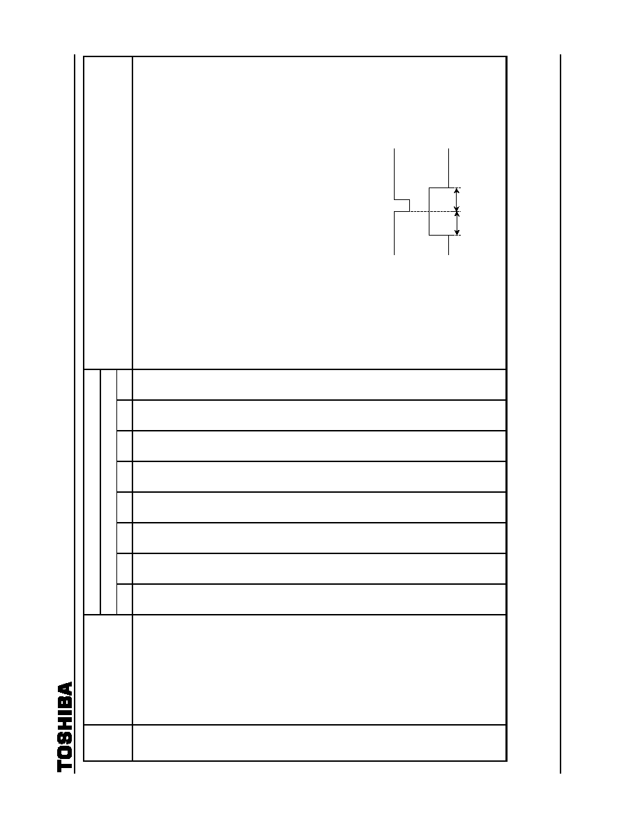
TA1317AN
2002-09-06
53
Test Condition
SW Mode
Note
No.
Parameter
SW5 SW6 SW7 SW8 SW10
SW11
SW17
SW24
Test Method
(unless otherwise specified, V
CC
=
9 V, Ta
=
25
±
3∞C, data
=
preset values)
42
Analog blanking phase
ON
A
OFF
OFF
B
ON
A
A
(1) Input vertical trigger pulse to pin V
IN
.
Pulse
level
(VT)
=
3.0 V
(2) Set VD (sub-address: 00) to DC-Coupling mode (data: 80).
(3) Set V INTEGRAL CORRECTION (sub-address: 08) to center (data: 8F).
(4) Set V S CORRECTION (sub-address: 09) to center (data: A0).
(5) AS shown in the figure below, measure analog blanking phase in relation to pin 21
(V
IN
) under the following conditions.
(6) Set ANALOG V-BLK STOP PHASE (sub-address: 03) to minimum (data: 00) and
measure blanking phase BLHL.
(7) Set ANALOG V-BLK STOP PHASE (sub-address: 03) to center (data: 80) and
measure blanking phase BLHM.
(8) Set ANALOG V-BLK STOP PHASE (sub-address: 03) to maximum (data: F8) and
measure blanking phase BLHH.
(9) Set ANALOG V-BLK START PHASE (sub-address: 04) to minimum (data: 00) and
measure blanking phase BLLL.
(10) Set ANALOG V-BLK START PHASE (sub-address: 04) to center (data: 80) and
measure blanking phase BLLM.
(11) Set ANALOG V-BLK START PHASE (sub-address: 04) to maximum (data: F8) and
measure blanking phase BLLH.
Vertical trigger pulse
BLLL
BLLM
BLLH
Pin 20 (BLK OUT)
BLHL
BLHM
BLHH

TA1317AN
2002-09-06
54
Test Condition
SW Mode
Note
No.
Parameter
SW5 SW6 SW7 SW8 SW10
SW11
SW17
SW24
Test Method
(unless otherwise specified, V
CC
=
9 V, Ta
=
25
±
3∞C, data
=
preset values)
43 Parabola
amplitude
adjustment (EW parabola)
change amount at PWM
OFF
B
ON
ON
A
OFF
A
A
(1) Input vertical trigger pulse to pin V
IN
.
Pulse
level
(VT)
=
3.0 V
(2) Set PICTURE WIDTH (sub-address: 01) to maximum (data: 8C).
(3) Apply external power supply (DC voltage
=
7 V) to pin 3 (EHT IN).
(4) Set EW PARABOLA (sub-address: 0A) to minimum (data: 00) and measure Pin 10
(EW FD) amplitude V
PP
(00).
(5) Set EW PARABOLA (sub-address: 0A) to center (data: 20) and measure Pin 10
(EW FD) amplitude V
PP
(20).
(6) Set EW PARABOLA (sub-address: 0A) to maximum (data: 3F) and measure Pin 10
(EW FD) amplitude V
PP
(3F).
(7) Calculate change amount V
PP
using the following formula.
V
PP
=
V
PP
(3F)
-
V
PP
(00)
Pin 10 (EW FD) waveform
V
PP
(00)
V
PP
(3F
)

TA1317AN
2002-09-06
55
Test Circuit
200
18
12
11
1
2
3
5
4
6
7
8
9
10
13
14
24
23
22
20
21
15
19
18
17
16
V-
R
A
M
P
F
I
L
T
E
R
AG
C
F
I
L
T
E
R
V
REF
TC
FIL
T
E
R
V
IN
BL
K O
U
T
CE
NT
E
R
OUT
V-
D
F
O
U
T
LV
P
I
N
H-DF
OUT
DI
GI
T
A
L GND
SC
L
SD
A
V N
F
V
-
DC RE
F
CE
NT
E
R
DA
C
V
CC
EW
PW
M
EH
T IN
AN
AL
O
G
G
N
D
EW
F
D
V D
R
I
V
E
EW
F
I
L
T
E
R
FBP
IN
TA1317AN
24
23
22
21
20
19
17
16
15
14
13
Vin TP17
SCL
470
R14a
SDA
470
R13a
1
2
3
4
5
6
7
8
9
10
11
12
Hin
470
LED
47 k
R17
10 k
R20
20 k
R22
R24
0.
02
µ
F
C22
1
2
3
5
4
6
7
8
16
15
14
12
13
11
10
9
TC4538BP
1
µ
F
C23
1
µ
F
C24
M
C4
M
1
k
R4
Q6
1 k
R6a
10 k
R5a
3.
6 k
R5b
SW5
0.
01
µ
F
C7B
220
µ
F
C7A
SW6
C
A B
TP6
SW8
A B
SW10
SW11
2.
4 k
R8f
1
µ
F
C8
1 k
R10
Q10
SW12
0.
1
µ
F
C11
M
CTC7
CTC8
1200 pF
1000 pF
50 k
5.
1 k
RTC13
RTC14
51 k
RTC17
51 k
RTC18
10
µ
F
Pin
50 k
RT
C16
7.
5 k
RTC15
V
CC
V
CC
A B
SW24
A B
CT
C9
0.
1
µ
F
SW7
M
Mylar capacitor
M
SW17
M

TA1317AN
2002-09-06
56
Application Circuit 1
(V-AC coupling/EW parabola output)
12
11
1
2
3
5
4
6
7
8
9
10
13
14
24
23
22
20
21
15
19
18
17
16
V-
R
A
M
P
F
I
L
T
E
R
AG
C
F
I
L
T
E
R
V
REF
TC
FIL
T
E
R
V
IN
BL
K O
U
T
CE
NT
E
R
OUT
V-
D
F
O
U
T
L
VP IN
H-DF
OUT
DI
GI
T
A
L GND
SC
L
SD
A
V N
F
V
-
DC RE
F
CE
NT
E
R
DA
C
V
CC
EW
PW
M
EH
T IN
AN
AL
O
G
G
N
D
EW
F
D
V D
R
I
VE
EW
F
I
L
T
E
R
FBP
IN
TA1317AN
20 k
0.
02
µ
F
1
µ
F
1
µ
F
M
M
Mylar capacitor
M
10 k
400 k
18 k
+
200 V
0.
01
µ
F
130 k
0.
047
µ
F
270 k
2.2 M
330 k
+
B
390 k
F.B
.
T.
+
21 V
M
TA8427K
0.
01
µ
F
M
220
µ
F
+
9 V
33 k
27
k
7.
5 k
1.
2 k
+
27 V
0.
1
µ
F
M
-
27 V
H-OUT
M

TA1317AN
2002-09-06
57
Application Circuit 2
(V-DC coupling/EW PWM output)
FBP (Pin 12)
H ramp (Internal signal)
H ramp
EW PWM (Pin 8)
EW parabola (Pin 11)
12
11
1
2
3
5
4
6
7
8
9
10
13
14
24
23
22
20
21
15
19
18
17
16
V-
R
A
M
P
F
I
L
T
E
R
AG
C
F
I
L
T
E
R
V
REF
TC
FIL
T
E
R
V
IN
BL
K O
U
T
CE
NT
E
R
OUT
V-
D
F
O
U
T
LV
P
I
N
H-DF
OUT
DI
GI
T
A
L GND
SC
L
SD
A
V N
F
V
-
DC RE
F
CE
NT
E
R
DA
C
V
CC
EW
PW
M
EH
T IN
A
N
A
L
OG
GND
EW
F
D
V D
R
I
VE
EW
F
I
L
T
E
R
FBP
IN
TA1317AN
20 k
0.
02
µ
F
1
µ
F
1
µ
F
M
M
Mylar capacitor
M
10 k
400 k
18 k
+
200 V
0.
01
µ
F
130 k
0.
047
µ
F
270 k
2.2 M
330 k
+
B
390 k
F.B
.
T.
+
21 V
M
0.
01
µ
F
220
µ
F
+
9 V
H-OUT
S
D
G
-
B
DY
10 k
10 k
TA8427K
1 k
0.
056
µ
F
10 k
3900 pF
1200 pF
+
25 V
M

TA1317AN
2002-09-06
58
Package Dimensions
Weight: 1.22 g (typ.)

TA1317AN
2002-09-06
59
∑
TOSHIBA is continually working to improve the quality and reliability of its products. Nevertheless, semiconductor
devices in general can malfunction or fail due to their inherent electrical sensitivity and vulnerability to physical
stress. It is the responsibility of the buyer, when utilizing TOSHIBA products, to comply with the standards of
safety in making a safe design for the entire system, and to avoid situations in which a malfunction or failure of
such TOSHIBA products could cause loss of human life, bodily injury or damage to property.
In developing your designs, please ensure that TOSHIBA products are used within specified operating ranges as
set forth in the most recent TOSHIBA products specifications. Also, please keep in mind the precautions and
conditions set forth in the "Handling Guide for Semiconductor Devices," or "TOSHIBA Semiconductor Reliability
Handbook" etc..
∑
The TOSHIBA products listed in this document are intended for usage in general electronics applications
(computer, personal equipment, office equipment, measuring equipment, industrial robotics, domestic appliances,
etc.). These TOSHIBA products are neither intended nor warranted for usage in equipment that requires
extraordinarily high quality and/or reliability or a malfunction or failure of which may cause loss of human life or
bodily injury ("Unintended Usage"). Unintended Usage include atomic energy control instruments, airplane or
spaceship instruments, transportation instruments, traffic signal instruments, combustion control instruments,
medical instruments, all types of safety devices, etc.. Unintended Usage of TOSHIBA products listed in this
document shall be made at the customer's own risk.
∑
The products described in this document are subject to the foreign exchange and foreign trade laws.
∑
The information contained herein is presented only as a guide for the applications of our products. No
responsibility is assumed by TOSHIBA CORPORATION for any infringements of intellectual property or other
rights of the third parties which may result from its use. No license is granted by implication or otherwise under
any intellectual property or other rights of TOSHIBA CORPORATION or others.
∑
The information contained herein is subject to change without notice.
000707EBA
RESTRICTIONS ON PRODUCT USE

This datasheet has been download from:
www.datasheetcatalog.com
Datasheets for electronics components.