 | –≠–ª–µ–∫—Ç—Ä–æ–Ω–Ω—ã–π –∫–æ–º–ø–æ–Ω–µ–Ω—Ç: TA2149BFN | –°–∫–∞—á–∞—Ç—å:  PDF PDF  ZIP ZIP |

TA2149BN/BFN
2001-12-21
1
TOSHIBA Bipolar Linear Integrated Circuit Silicon Monolithic
TA2149BN,TA2149BFN
3 V AM/FM 1 Chip Tuner IC (for Digital Tuning System)
TA2149BN, TA2149BFN are AM/FM 1 chip tuner ICs, which
are designed for portable Radios and 3 V Head phone Radios.
This is suitable for Digital Tuning System Applications. FM
Local Oscillation Voltage is set up low relativity, for NEW FCC.
Functions
∑ For NEW FCC.
∑ Suitable for combination with Digital Tuning System which is
included IF Counter.
∑ Adjustable for IF count output sensitivity by external
resistance of pin 17 (FM only).
∑ One terminal type AM/FM IF count output for IF counter of
Digital Tuning System.
∑ FM: 1.3375 MHz (1/8 dividing)
∑ AM: 450 kHz
∑ Built-in Mute Circuit for IF count output.
∑ For adopting ceramic Discriminator, it is not necessary to
adjust the FM Quad Detector Circuit.
∑ Built-in FM MPX VCO circuit.
∑ Built-in one terminal type AM/FM Local Oscillator Buffer
Output for Digital Tuning System Applications.
∑ Built-in 1/16 Pre-scaler for FM Local OSC Buffer.
∑ Built-in AM Low cut circuit.
∑ Low supply current.
(V
CC
= 3 V, Ta = 25∞C)
I
CCq
(FM) = 13 mA (Typ.)
I
CCq
(AM) = 8.5 mA (Typ.)
∑ Operating Supply voltage range: V
CC
= 1.8~7 V (Ta = 25∞C)
Note 1: Handle with care to prevent devices from deteriorations by static electricity.
TA2149BN
TA2149BFN
Weight
SDIP24-P-300-1.78: 1.2 g (Typ.)
SSOP24-P-300-0.65A: 0.14 g (Typ.)

TA2149BN/BFN
2001-12-21
2
Block Diagram
LPF1
24
23
22
21
18
17
16
15
14
13
19
FM
RFout
RF
V
CC
AM
RFin
FM
OSC
AM
OSC
OSC
OUT
ST
LED
IF
REQ
DET
OUT
MPX
IN LPF2
AM
LOW
CUT
20
AM
OSC
FM
OSC
BUFF
BUFF
1/1 or
1/16
ST
SW
IF
REQ
IF
BUFF
1/8
LEVEL
DET
AF
BUFF
AM
DET
FM
DET
FMIF
AMIF
AGC
AM
MIX
FM
MIX
FMRF
AF
VCO
DIVIDE
DECODE
SM/MO
FM/AM
MUTE
1
2
3
4
8
9
10
11
12
RF
GND
FM
RFin
MIX
OUT
V
CC
AM IF
IN
FM IF
IN
GND
AGC
QUAD R-OUT L-OUT
5
7
6
V
CC
BFP
R-OUT L-OUT
FM
ANTENNA
IF REQ
IF OUT
V
T
OSC BUFF OUT
PSC SW
OPEN: 1/1
V
CC
: 1/16
H: MONO
L: ST
H: AM
L: FM

TA2149BN/BFN
2001-12-21
3
Explanation of Terminals
(Terminal Voltage: Typical terminal voltage at no signal with test circuit,
V
CC
=
=
=
=
3 V, Ta
=
=
=
=
25
∞
∞
∞
∞
C)
Terminal Voltage
(Typ.) (V)
PIN
No.
Characteristic Internal
Circuit
AM FM
1
RF GND
(GND for FM RF stage)
æ
0 0
2 FM-RFin
0 0.8
3
AM LOW CUT
1.0
æ
4 MIX
OUT
3.0 3.0
5
V
CC
(V
CC
for AM, FM IF, MPX)
æ
3.0
3.0
6 AM
IF
IN
2.3 2.5
V
CC
5
1
8
4
FM
MIX
RF GND
AM
MIX
GND
6
GND 8
3 k
W
3 k
W
1
24
2
1 k
W
60 pF
RF GND
8
3
22 k
W
AM
DET
22 k
W
GND

TA2149BN/BFN
2001-12-21
4
Terminal Voltage
(Typ.) (V)
PIN
No.
Characteristic Internal
Circuit
AM FM
7 FM
IF
IN
3.0 3.0
8
GND
(GND for AM, FM IF, MPX)
æ
0
0
9 AGC
0 0
10 QUAD
2.5 2.2
11
12
R-OUT
L-OUT
1.2 1.2
5
8
10
GND
V
CC
8
9
GND
5
V
CC
20 k
W
100 k
W
5
8
V
CC
GND
5 k
W
11/12
V
CC
5
7
GND 8
330
W

TA2149BN/BFN
2001-12-21
5
Terminal Voltage
(Typ.) (V)
PIN
No.
Characteristic Internal
Circuit
AM FM
13
LPF2
∑
LPF terminal for phase
detector
∑
Bias terminal AM/FM SW
circuit
V
13
=
GND
Æ
AM
V
13
=
OPEN
Æ
FM
0 2.2
14
LPF1
∑
LPF terminal for
synchronous detector
∑
VCO stop terminal
V
14
=
GND
Æ
VCO
STOP
0.7 2.4
15 MPX
IN
0.7 0.7
16 DET
OUT
1.0 0.9
8 GND
DC
AMP
14
8 GND
AM/FM
SW
13
15
8
55 k
W
GND
5
8
a
b
16
FM
AM
GND
750
W
LOW
Æ
FM, HIGH
Æ
AM
LOW
Æ
AM, HIGH
Æ
FM
a
b
V
CC

TA2149BN/BFN
2001-12-21
6
Terminal Voltage
(Typ.) (V)
PIN
No.
Characteristic Internal
Circuit
AM FM
17 IF
REQ
æ
æ
18 ST
LED
æ
æ
19 OSC
OUT
2.8 2.7
20 AM
OSC
3.0 3.0
21 FM
OSC
3.0 3.0
GND
18
19 kHz
8
5
8
20
V
CC
GND
5 V
CC
17
RF-GND
19
2
RF V
CC
23
200
W
PSC
SW
23
1
21
RF V
CC
GND

TA2149BN/BFN
2001-12-21
7
Terminal Voltage
(Typ.) (V)
PIN
No.
Characteristic Internal
Circuit
AM FM
22 AM
RFin
3.0 3.0
23
RF V
CC
(V
CC
for FM RF stage)
æ
3.0
3.0
24
FM RFout
cf. pin 1
3.0
3.0
8
22
AGC
GND
5
V
CC

TA2149BN/BFN
2001-12-21
8
Application Note
1. AM Low-Cut Circuit
∑ The AM Low-Cut action is carried out by the bypass of the high frequency
component of the positive-feedback signal at the AF AMP stage.
The external capacitor: C
3
by-pass this component.
∑ The cut-off frequency fL is determined by the internal resistance
22 kW (Typ.) and the external capacitor C
3
as following;
(Hz)
C
10
22
2
1
f
3
3
L
¥
¥
¥
p
¥
=
∑ In the case of the AM Low-Cut function is not needed, set up the value of C
3
over 1 mF.
In the condition of C
3
>
= 1 mF, the frequency characteristic has flat response at the low frequency.
∑ It is possible to reduce the recovered output level at AM mode, by additional resistance between the pin 3
and GND line.
2. FM Detection Circuit
For the FM detection circuit, detection coil is able to use instead of ceramic discriminator.
Recommended circuit and recommended coil are as follows. (In this case, please take care that V
in
(lim.)
falls a little.)
Turns
Test
Frequency
Co
(pF)
Qo
1-2
2-3
1-3
4-6
Wire
(mm
f
)
Reference
10.7 MHz
51
45
æ
æ
30
æ
0.08UEW
Toko Co., Ltd.
600BEAS-10018Z
3. FM/AM switch and forced monaural switch.
∑ FM/AM switchover and stereo/forced monaural switchover are done by pin 13 and pin 14.
∑ FM/AM switch (pin 13)
V13: Low (Active Low, V
th
= 0.2 V (Typ.), I
th
30 mA (Typ.) Æ AM
V13: OPEN
Æ FM
∑ Stereo/forced monaural switch (pin 14)
V14: Low (Active Low, V
th
= 0.2 V (Typ.), I
th
30 mA (Typ.)Æ Forced Monaural
V14: OPEN
Æ Stereo
V
CE (sat)
14
13
V
CE (sat)
V
CC
3
22 k
W
22 k
W
R
C
3
3
1
2
4
6
V
CC
Pin 10
10
15 P
V
CC

TA2149BN/BFN
2001-12-21
9
4. V
CC
Line
This ICs have two voltage supply terminals, V
CC
(for AM, FM IF, MPX stage) and RF V
CC
(for FM RF
stage). Set up the potential difference between V
CC
and RF V
CC
0.4 V (typ.) or less, otherwise there is the
case that this IC doesn't operate normally.
5. How to control the Divider of FM OSC.
Divider of FM OSC ON/OFF switching is controlled by external pull-up resistor of pin 19.
In case of Divider of FM OSC is used, it is necessary to set up the value of R under 470 W (typ.).
When R is over 470 W, it is feared that Divider is not operating. (At this time, buffer output frequency is
equal to FM OSC frequency.)
Which ever Divider of FM OSC is used or not, AM OSC buffer frequency and output level is same.
Mode SW8 Output
Frequency Output
Level
(Typ.)
OPEN
1/1 FM OSC
35 mVrms
FM
ON 1/16
FM
OSC 110
mVrms
OPNE
AM
ON
1/1 FM OSC
75 mVrms
6. How to adjust the IF Count Output Sensitivity
IF count output sensitivity can be adjusted by changing the value of external resistance at pin 17.
This ICs have IF signal level detector in pin 9. When DC voltage of pin 9 is high than threshold, IF count
output signal come out from the pin 17.
And this threshold is controlled by value of external resistance at pin 19.
SW8
AM
OSC
FM
OSC
buff
buff
1/1
or
1/16
19
R
buff out
RF V
CC
External resistance of pin-17 (k
9
)
IF c
o
u
n
t o
u
t
put
vol
t
ag
e
V
IF
(FM
)
mV
p-p
IF
c
o
u
n
t
o
u
t
put
sen
s
itivity
IF
se
ns
(F
M)
40
0
45
50
55
65
60
0.5 1.5
2
3
3.5
1
2.5
0
50
100
150
350
200
IF sens (FM)
VIF (FM)
250
300
30
35
VCC
=
3 V
f
=
10.7 MHz
D
f
=
75 MHz

TA2149BN/BFN
2001-12-21
10
Maximum Ratings
(Ta
=
=
=
=
25∞C)
Characteristics Symbol
Rating
Unit
Supply voltage
V
CC
8 V
LED current
ILED
10
mA
LED voltage
VLED
8
V
TA2149BN 1200
Power dissipation
TA2149BFN
P
D
(Note 2)
500
mW
Operating temperature
T
opr
-
25~75 ∞C
Storage temperature
T
stg
-
55~150 ∞C
Note 2: Derated above Ta
=
25∞C in the proportion of 9.6 mW/∞C for TA2149BN of 4 mW/∞C for TA2149BFN.
Electrical Characteristics
(Unless otherwise specified, Ta
=
=
=
=
25∞C, V
CC
=
=
=
=
3 V,
F/E:
f
=
=
=
=
98 MHz, f
m
=
=
=
=
1 kHz
FM
IF:
f
=
=
=
=
10.7 MHz,
D
D
D
D
f
=
=
=
=
±
±
±
±
75 kHz, f
m
=
=
=
=
1 kHz
AM:
f
=
=
=
=
1 MHz, MOD
=
=
=
=
30%, f
m
=
=
=
=
1 kHz
MPX:
f
m
=
=
=
=
1 kHz)
Characteristic Symbol
Test
Circuit
Test Condition
Min
Typ.
Max
Unit
I
CC (FM)
æ
V
in
=
0, FM mode
æ
13 16.5
Supply current
I
CC (AM)
æ
V
in
=
0, AM mode
æ
8.5 11.0
mA
Input limiting voltage
V
in (lim)
æ
V
in
=
60dB
m
V EMF,
-
3dB limiting
æ
10
æ
dB
m
V EMF
Local OSC buffer output
voltage 1
V
OSC
(buff) FM1
æ
f
OSC
=
108.7 MHz
23
35
æ
mVrms
F/E
Local OSC buffer output
voltage 2
V
OSC
(buff) FM2
æ
f
OSC
=
6.79375 MHz
SW8: ON
75 110
æ
mVrms
Input limiting voltage
V
in (lim) IF
æ
V
in
=
80dB
m
V EMF,
-
3dB limiting
37 42 47
dB
m
V EMF
Recovered output voltage
V
OD
æ
V
in
=
80dB
m
V EMF
200
250
300
mVrms
Signal to noise ratio
S/N
æ
V
in
=
80dB
m
V EMF
æ
75
æ
dB
Total harmonic distortion
THD
æ
V
in
=
80dB
m
V EMF
æ
0.3
æ
%
AM rejection ration
AMR
æ
V
in
=
80dB
m
V EMF
æ
60
æ
dB
IF count output frequency
f
IF
(FM)
æ
V
in
=
80dB
m
V EMF, SW7: ON 1.3373 1.3375 1.3377
MHz
IF count output voltage
V
IF
(FM)
æ
V
in
=
80dB
m
V EMF, SW7: ON
250
290
330
mV
p-p
FM IF
IF count output sensitivity
IF sens
(FM)
æ
SW7:
ON
42
47
52 dB
m
V EMF
Gain G
V
æ
V
in
=
27dB
m
V EMF
20
38
70
mVrms
Recovered output voltage
V
OD
æ
V
in
=
60dB
m
V EMF
60
85
108
mVrms
Signal to noise ratio
S/N
æ
V
in
=
60dB
m
V EMF
æ
41
æ
dB
Total harmonic distortion
THD
æ
V
in
=
60dB
m
V EMF
æ
0.7
æ
%
Local OSC buffer output
voltage
V
OSC
(buff) AM
æ
f
OSC
=
1.45 MHz
55
75
æ
mVrms
IF count output voltage
V
IF
(AM)
æ
V
in
=
60dB
m
V EMF
SW7: ON
250
290
350
mV
p-p
AM
IF count output sensitivity
IF sens
(AM)
æ
SW7:
ON
33
38
43 dB
m
V EMF
æ
FM
mode
æ
0.75
æ
Pin 17 output resistance
R
17
æ
AM
mode
æ
15.5
æ
k
W

TA2149BN/BFN
2001-12-21
11
Characteristic Symbol
Test
Circuit
Test Condition
Min
Typ.
Max
Unit
Input resistance
R
IN
æ
æ
æ
55
æ
k
W
Output resistance
R
OUT
æ
æ
æ
5
æ
k
W
Max. composite signal input
voltage
V
in MAX
(Stereo)
æ
L
+
R
=
90%, P
=
10%,
SW3: LPF ON
f
m
=
1 kHz, THD
=
3%
æ
700
æ
mVrms
f
m
=
100 Hz
æ
45
æ
f
m
=
1 kHz
35
45
æ
Separation Sep.
æ
L
+
R
=
180 mVrms,
P
=
20 mVrms
SW3: LPF ON
f
m
=
10 kHz
æ
45
æ
dB
Monaural
THD
(Monaural)
æ
V
in
=
200 mVrms
æ
0.3
æ
Total harmonic
distortion
Stereo
THD
(Stereo)
æ
L+R
=
180 mVrms,
P
=
20 mVrms, SW3: LPF ON
æ
0.3
æ
%
Voltage gain
G
V
æ
V
in
=
200 mVrms
-
2.7
-
1.2 0.2
dB
Channel balance
C.B.
æ
V
in
=
200 mVrms
-
1.5 0 1.5 dB
ON V
L (ON)
æ
æ
10 14
Stereo LED
sensitivity
OFF V
L (OFF)
æ
Pilot input (19 kHz)
5 8
æ
mVrms
Stereo LED hysteresis
V
H
æ
To LED turn off from LED turn
on
æ
2
æ
mVrms
Capture range
C.R.
æ
P
=
15 mVrms
æ
±
8
æ
%
MPX
Signal noise ratio
S/N
æ
V
in
=
200 mVrms
æ
80
æ
dB
Muting attenuation
MUTE
æ
V
in
=
200 mVrms
æ
80
æ
dB
Coil Data
Turns
Coil No.
Test Freq.
L
(
m
H)
Co
(pF)
Qo
1-2
2-3
1-3
1-4
4-6
Wire
(mm
f
)
Reference
L
1
FM RF
100 MH
æ
æ
79
æ
æ
2
1
2
æ
æ
0.16UEW Toko Co., Ltd.
666SNF-305NK
L
2
FM OSC 100 MH
æ
æ
76
æ
æ
2
æ
æ
0.16UEW Toko Co., Ltd.
666SNF-306NK
T
1
AM OSC 796 kH
268
æ
65
19
95
æ
æ
æ
0.05UEW Toko Co., Ltd.
5PNR-5146Y
T
2
AM IFT
455 kH
æ
470 60
æ
æ
109
æ
7
0.05UEW
Toko Co., Ltd.
5PLG-5147X
3
1
L
1
: FM RF
3
1
L
2
: FM OSC
T
1
: AM OSC
3
1
2
4
6
V
CC
Pin 20
T
2
: AM IFT
3
1
2
4
6
V
CC
AM C.F.
FM C.F.
Pin 4

TA2149BN/BFN
2001-12-21
12
Test Circuit
24
23
L
1
22
2.
7 m
H
100 pF
47 k
W
1S
V
101
21
L
2
1000 pF
47 k
W
1S
V
101
20
T
1
1S
V
149
470 pF
47 k
W
18
17
16
15
14
13
19
470
W
SW
8
560
W
3.
3 k
W
SW
7
330 pF
3.
3 k
W
SW
5
0.
1
m
F
SW
4
220
m
F
V
CC
FM RFout RF V
CC
AM RFin FM OSC AM OSC
OSC
OUT
ST LED IF REQ DET OUT MPX IN
LPF1
LPF2
1
2
3
4
8
9
10
11
12
1
m
F
0.
1
m
F
10
m
F MPX IN
RF
GND
FM RFin
AM LOW
CUT MIX OUT
V
CC
AM IF IN FM IF IN
GND
AGC
QUAD
R-OUT
L-OUT
5
7
6
0.
47
m
F
4.
7
m
F
0.033
m
F
CF
1
CF
2
T
2
330
W
CR
1
m
F
0.
01
m
F
0.
01
m
F
SW
2
LPF
SW
3
BPF
FM-RF IN
FM-IF IN
270
W
50
W
75
W
Vin
Vin
SW
1
V
T
75
W
Vin
400
W
OSC OUT
2 k
W
75
W
AM-RF IN
V
DD
=
8 V
IF OUT
3 k
W
100 k
W
0.
01
m
F
100 k
W
110 k
W
110
k
W
5 V
2.
2 k
W
2.4 k
W
0.
022
m
F
DET OUT
BPF : GFWB3 (Soshin Electric Co., Ltd.)
CF
1
: SFU450B (Murata Co., Ltd.)
CF
2
: SFE10.7MA5 (Murata Co., Ltd.)
CR : CDALA10M7GA100A-B0 (Murata Co., Ltd.)
TA2149BN/BFN
2S
C1815
2S
C1923
4.
7 k
W
0.
01
m
F
0.022
m
F
2.
2
m
F

TA2149BN/BFN
2001-12-21
13
Package Dimensions
Weight: 1.2 g (typ.)
TA2149BN/BFN
2001-12-21
14
Package Dimensions
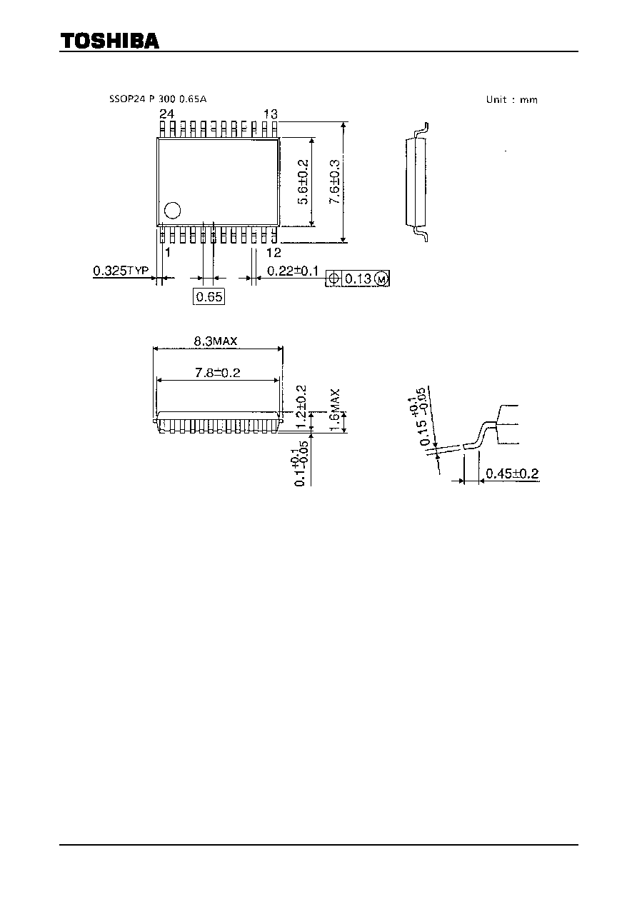
Weight: 0.14 g (typ.)

TA2149BN/BFN
2001-12-21
15
∑
TOSHIBA is continually working to improve the quality and reliability of its products. Nevertheless, semiconductor
devices in general can malfunction or fail due to their inherent electrical sensitivity and vulnerability to physical
stress. It is the responsibility of the buyer, when utilizing TOSHIBA products, to comply with the standards of
safety in making a safe design for the entire system, and to avoid situations in which a malfunction or failure of
such TOSHIBA products could cause loss of human life, bodily injury or damage to property.
In developing your designs, please ensure that TOSHIBA products are used within specified operating ranges as
set forth in the most recent TOSHIBA products specifications. Also, please keep in mind the precautions and
conditions set forth in the "Handling Guide for Semiconductor Devices," or "TOSHIBA Semiconductor Reliability
Handbook" etc..
∑
The TOSHIBA products listed in this document are intended for usage in general electronics applications
(computer, personal equipment, office equipment, measuring equipment, industrial robotics, domestic appliances,
etc.). These TOSHIBA products are neither intended nor warranted for usage in equipment that requires
extraordinarily high quality and/or reliability or a malfunction or failure of which may cause loss of human life or
bodily injury ("Unintended Usage"). Unintended Usage include atomic energy control instruments, airplane or
spaceship instruments, transportation instruments, traffic signal instruments, combustion control instruments,
medical instruments, all types of safety devices, etc.. Unintended Usage of TOSHIBA products listed in this
document shall be made at the customer's own risk.
∑
The products described in this document are subject to the foreign exchange and foreign trade laws.
∑
The information contained herein is presented only as a guide for the applications of our products. No
responsibility is assumed by TOSHIBA CORPORATION for any infringements of intellectual property or other
rights of the third parties which may result from its use. No license is granted by implication or otherwise under
any intellectual property or other rights of TOSHIBA CORPORATION or others.
∑
The information contained herein is subject to change without notice.
000707EBA
RESTRICTIONS ON PRODUCT USE